functions – pulsewidth modulation techniques – are man- ifold. They range from
simple ... Three-phase electronic power converters controlled by pulsewidth ...
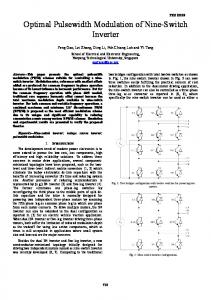
Lerb
Pulsewidth Modulation for Electronic Power Conversion J. Holtz, Fellow, IEEE Wuppertal University – Germany
Abstract – The efficient and fast control of electric power forms part of the key technologies of modern automated production. It is performed using electronic power converters. The converters transfer energy from a source to a controlled process in a quantized fashion, using semiconductor switches which are turned on and off at fast repetition rates. The algorithms which generate the switching functions – pulsewidth modulation techniques – are manifold. They range from simple averaging schemes to involved methods of real-time optimization. This paper gives an overview.
1. INTRODUCTION Many three-phase loads require a supply of variable voltage at variable frequency, including fast and high-efficiency control by electronic means. Predominant applications are in variable speed ac drives, where the rotor speed is controlled through the supply frequency, and the machine flux through the supply voltage. The power requirements for these applications range from fractions of kilowatts to several megawatts. It is preferred in general to take the power from a dc source and convert it to three-phase ac using power electronic dc-to-ac converters. The input dc voltage, mostly of constant magnitude, is obtained from a public utility through rectification, or from a storage battery in the case of an electric vehicle drive. The conversion of dc power to three-phase ac power is exclusively performed in the switched mode. Power semiconductor switches effectuate temporary connections at high repetition rates between the two dc terminals and the three phases of the ac drive motor. The actual power flow in each motor phase is controlled by the on/off ratio, or duty-cycle, of the respective switches. The desired sinusoidal waveform of the currents is achieved by varying the duty-cycles sinusoidally with time, employing techniques of pulsewidth modulation (PWM). The basic principle of pulsewidth modulation is characterized by the waveforms in Fig. 1. The voltage waveform
ud /2 0 -ud /2
uL1
a)
ud /2 usα 0 -ud /2
b)
isα
15 A 0
j Im As
current densitiy distribution
i sb
j
j i sc
Re i sb
i sc
i s = is exp(jj)
j Im
i sa
i sa Re
a)
b)
Fig. 2: Definition of a current space vector; (a) cross section of an induction motor, (b) stator windings and stator current space vector in the complex plane at one inverter terminal, Fig. 1(a), exhibits the varying duty-cycles of the power switches. The waveform is also influenced by the switching in other phases, which creates five distinct voltage levels, Fig. 1(b). Further explanation is given in Section 2.3. The resulting current waveform Fig. 1(c) exhibits the fundamental content more clearly, which is owed to the low-pass characteristics of the machine. The operation in the switched mode ensures that the efficiency of power conversion is high. The losses in the switch are zero in the off-state, and relatively low during the on-state. There are switching losses in addition which occur during the transitions between the two states. The switching losses increase with switching frequency. As seen from the pulsewidth modulation process, the switching frequency should be preferably high, so as to attenuate the undesired side-effects of discontinuous power flow at switching. The limitation of switching frequency that exists due to the switching losses creates a conflicting situation. The tradeoff which must be found here is strongly influenced by the respective pulsewidth modulation technique. Three-phase electronic power converters controlled by pulsewidth modulation have a wide range of applications for dc-to-ac power supplies and ac machine drives. Important quantities to be considered with machine loads are the two-dimensional distributions of current densities and flux linkages in ac machine windings. These can be best analyzed using the space vector approach, to which a short introduction will be given first. Performance criteria will be then introduced to enable the evaluation and comparison of different PWM techniques. The following sections are organized to treat open-loop and closed-loop PWM schemes. Both categories are subdivided into nonoptimal and optimal strategies.
c)
2. AN I NTRODUCTION TO SPACE VECTORS
-15 A 0
10
t
20 ms
Fig. 1: Recorded three-phase PWM waveforms (suboscillation method); (a) voltage at one inverter terminal, (b) phase voltage usα , (c) load current isα
2.1 Definitions Consider a symmetrical three-phase winding of an electric machine, Fig. 2(a), reduced to a two-pole arrangement for simplicity. The three phase axes are defined by the unity vectors, 1, a, and a2, where a = exp(2π/3). Neglecting space harmonics, a sinusoidal current density distribution is es-
Proceedings of the IEEE, Vol. 82, No. 8, Aug. 1994, pp. 1194 - 1214
-2tablished around the air-gap by the phase currents isa, isb, and isc as shown in Fig. 2(b). The wave rotates at the angular frequency of the phase currents. Like any sinusoidal distribution in time and space, it can be represented by a complex phasor As as shown in Fig. 2(a). It is preferred, however, to describe the mmf wave by the equivalent current phasor is, because this quantity is directly linked to the three stator currents isa, isb, isc that can be directly measured at the machine terminals:
is =
(
2 i + a isb + a 2 isc 3 sa
)
(1)
The subscript s refers to the stator of the machine. The complex phasor in (1), more frequently referred to in the literature as a current space vector [1], has the same direction in space as the magnetic flux density wave produced by the mmf distribution As. A sinusoidal flux density wave can be also described by a space vector. It is preferred, however, to choose the corresponding distribution of the flux linkage with a particular three-phase winding as the characterizing quantity. For example, we write the flux linkage space vector of the stator winding in Fig. 2 as y s = ls is
(2)
In the general case, when the machine develops nonzero torque, both space vectors is of the stator current, and ir of the rotor current are nonzero, yielding the stator flux linkage vector as ys = ls is + lh ir
(3)
where ls is the equivalent stator winding inductance and lh the composite mutual inductance between the stator and rotor windings. Furthermore,
ir =
(
2 i + a irb + a 2 irc 3 ra
)
(4)
is the rotor current space vector, ira, irb and irc are the three rotor currents. Note that flux linkage vectors like y s also represent sinusoidal distributions in space, which can be seen from an inspection of (2) or (3). The rotating stator flux linkage wave y s generates induced voltages in the stator windings which are described by dys , (5) us = dt where 2 us = u + a usb + a 2 usc (6) 3 sa
(
)
is the space vector of the stator voltages, and usa, u sb, u sc are the stator phase voltages. The individual phase quantities associated to any space vector are obtained as the projections of the space vector on the respective phase axis. Given the space vector us , for example, we obtain the phase voltages as usa = Re {us }
{
usb = Re a 2 . us
}
(7)
usc = Re {a . us }
Considering the case of three-phase dc-to-ac power supplies, an LC-filter and the connected load replace the motor at the inverter output terminals. Although not distributed in space, such load circuit behaves exactly the same way as a motor load. It is permitted and common practice therefore
to extend the space vector approach to the analysis of equivalent lumped parameter circuits. 2.2 Normalization Normalized quantities are used throughout this paper. Space vectors are normalized with reference to the nominal values of the connected ac machine. The respective base quantities are • the rated peak phase voltage 2 Uph R, (8) • the rated peak phase current 2 I ph R, and ωsR. • the rated stator frequency Using the definition of the maximum modulation index in section 4.1.1, the normalized dc bus voltage of a dc link inverter becomes ud = π/2. 2.3 Switching state vectors The space vector resulting from a symmetrical sinusoidal voltage system usa, usb, u sc of frequency ωs is
us = us . exp ( jwst ) ,
(9)
which can be shown by inserting the phase voltages (7) into (6). A three-phase machine being fed from a switched power converter Fig. 3 receives the symmetrical rectangular threephase voltages shown in Fig. 4. The three phase potentials Fig. 4(a) are constant over every sixth of the fundamental period, assuming one of the two voltage levels, +Ud/2 or – Ud/2, at a given time. The neutral point potential unp , Fig. 3, of the load is either positive, when more than one upper half-bridge switch is closed, Fig. 4(b); it is negative with more than one lower half-bridge switch closed. The respective voltage levels shown in Fig. 4(b) hold for symmetrical load impedances.
1U 2 d
S1
S2
S3
1U 2 d
S4
S5
S6
u L1 u np
L1
L2
ua
L3
ub
uc
Fig. 3: Three-phase power converter; the switch pairs S1 – S4 (and S2 – S5, and S3 – S6) form half-bridges; one, and only one switch in a half bridge is closed at a time. The waveform of the phase voltage ua = uL1 – unp is displayed in the upper trace of Fig. 4(c). It forms a symmetrical, nonsinusoidal three-phase voltage system along with the other phase voltages ub and uc. Since the waveform u np has three times the frequency of uLi , i = 1, 2, 3, while its amplitude equals exactly one third of the amplitudes of uLi, this waveform contains exactly all triplen of the harmonic components of u Li . Because of ua = uL1 – unp there are no triplen harmonics left in the phase voltages. This is also true for the general case of three-phase symmetrical pulsewidth modulated waveforms. As all triplen harmonics form zero-sequence systems, they produce no currents in the machine windings, provided there is no electrical connection to the star-point of the load, i. e. unp in Fig. 3 must not be shorted. The example Fig. 4 demonstrates also that a change of
-31
u L1
3
4
5
losses of the machine, which account for a major portion of the machine losses. The rms harmonic current
6
0
1u 2 d
u L2
0
u L3
0
unp
2
1u 2 d
a)
2π
1u 6 d
2π
b)
2u 3 d
ua
0 2u 3 d
ub
0
uc
0
1 i(t ) − i1 (t )]2 dt T ∫T [
Ih rms =
c)
2π
does not only depend on the performance of the pulsewidth modulator, but also on the internal impedance of the machine. This influence is eliminated when using the distortion factor Ih rms (11) d= Ih rms six −step as a figure of merit. In this definition, the distortion current Ihrms (10) of a given switching sequence is referred to the distortion current I h rms six-step of same ac load operated in the six-step mode, i. e. with the unpulsed rectangular voltage waveforms Fig. 4(c). The definition (11) values the ac-side current distortion of a PWM method independently from the properties of the load. We have d = 1 at six-step operation by definition. Note that the distortion factor d of a pulsed waveform can be much higher than that of a rectangular wave, e. g. Fig. 19. The harmonic content of a current space vector trajectory is computed as
wt
Fig. 4: Switched three-phase waveforms; (a) voltage potentials at the load terminals, (b) neutral point potential, (c) phase voltages any half-bridge potential invariably influences upon the other two-phase voltages. It is therefore expedient for the design of PWM strategies and for the analysis of PWM waveforms to analyse the three-phase voltages as a whole, instead of looking at the individual phase voltages separately. The space vector approach complies exactly with this requirement. Inserting the phase voltages Fig. 4(c) into (6) yields the typical set of six active switching state vectors u1 ... u6 shown in Fig. 5. The switching state vectors describe the inverter output voltages. At operation with pulsewidth modulated waveforms, the two zero vectors u0 and u7 are added to the pattern in Fig. 5. The zero vectors are associated to those inverter states with all upper half-bridge switches closed, or all lower, respectively. The three machine terminals are then short-circuited, and the voltage vector assumes zero magnitude. Using (7), the three phase voltages of Fig. 4(c) can be reconstructed from the switching state pattern Fig. 5.
3. PERFORMANCE CRITERIA Considering an ac machine drive, it is the leakage inductances of the machine and the inertia of the mechanical system which account for low pass filtering of the harmonic components contained in the switched voltage waveforms. Remaining distortions of the current waveforms, harmonic losses in the power converter and the load, and oscillations in the electromagnetic machine torque are due to the operation in the switched mode. They can be valued by performance criteria [2] ... [7]. These provide the means of comparing the qualities of different PWM methods and support the selection of a pulsewidth modulator for a particular application. 3.1 Current harmonics The harmonic currents primarily determine the copper
(10)
Ih rms =
1 (i(t ) − i1 (t )) ⋅ (i(t ) − i1 (t )) * dt T ∫T
(12)
from which d can be determined by (11). The asterisc in (12) marks the complex conjugate. The harmonic copper losses in the load circuit are proportional to the square of the harmonic current: PLc ∝ d 2, where d 2 is the loss factor. ( + ) jIm
(+ + )
u2
u3
2u
( + +)
u1 3
u4
Re
(
+)
u5
u6
d
(+
)
u 7 (+ + +) ) u 0 (
(+ +)
Fig. 5: Switching state vectors in the complex plane; in brackets: switching polarities of the three half-bridges 3.2 Harmonic spectrum The contributions of individual frequency components to a nonsinusiodal current wave are expressed in a harmonic current spectrum, which is a more detailed description than the global distortion factor d. We obtain discrete current spectra hi (k . f1) in the case of synchronized PWM, where the switching frequency fs = N . f1 is an integral multiple of the fundamental frequency f1. N is the pulse number, or gear ratio, and k is the order of the harmonic component. Note that all harmonic spectra in this paper are normalized as per the definition (11):
hi ( k . f1 ) =
Ih rms ( k . f1 ) . Ih rms six-step
(13)
They describe the properties of a pulse modulation scheme independently from the parameters of the connected load. Nonsynchronized pulse sequences produce harmonic am-
-4plitude density spectra h d(f) of the currents, which are continuous functions of frequency. They generally contain periodic as well as nonperiodic components and hence must be displayed with reference to two different scale factors on the ordinate axis, e. g. Fig. 35. While the normalized discrete spectra do not have a physical dimension, the amplitude density sprectra are measured in Hz -1/2. The normalized harmonic current (11) is computed from the discrete spectrum (13) as d=
∑ hi 2 (k . f1 ) ,
k ≠1
(14)
and from the amplitude density spectrum as
d=
∞
∫
hd 2( f ) df .
0, f ≠ f1
(15)
Another figure of merit for a given PWM scheme is the product of the distortion factor and the switching frequency of the inverter. This value can be used to compare different PWM schemes operated at different switching frequencies provided that the pulse number N > 15. The relation becomes nonlinear at lower values of N. 3.3 Maximum modulation index The modulation index is the normalized fundamental voltage, defined as u1 (16) m= u1 six −step where u1 is the fundamental voltage of the modulated switching sequence and u1 six-step = 2/π . ud the fundamental voltage at six-step operation. We have 0 < m < 1, and hence unity modulation index, by definition, can be attained only in the six-step mode. The maximum value mmax of the modulation index may differ in a range of about 25% depending on the respective pulsewidth modulation method. As the maximum power of a PWM converter is proportional to the maximum voltage at the ac side, the maximum modulation index mmax constitutes an important utilization factor of the equipment. 3.4 Torque harmonics The torque ripple produced by a given switching sequence in a connected ac machine can be expressed as (17) ∆ T = (Tmax − Tav ) TR , where Tmax = maximum air-gap torque, Tav = average air-gap torque, TR = rated machine torque. Although torque harmonics are produced by the harmonic currents, there is no stringent relationship between both of them. Lower torque ripple can go along with higher current harmonics, and vice versa. 3.5 Switching frequency and switching losses The losses of power semiconductors subdivide into two major portions: The on-state losses
Pon = g1 (uon , iL ) , and the dynamic losses Pdyn = fs ⋅ g2 (U0 , iL ) .
(18a) (18b)
It is apparent from (18a) and (18b) that, once the power level has been fixed by the dc supply voltage U0 and the maximum load current iL max, the switching frequency fs is
an important design parameter. The harmonic distortion of the ac-side currents reduces almost linearly with this frequency. Yet the switching frequency cannot be deliberately increased for the following reasons:
•
The switching losses of semiconductor devices increase proportional to the switching frequency. • Semiconductor switches for higher power generally produce higher switching losses, and the switching frequency must be reduced accordingly. Megawatt switched power converters using GTO’s are switched at only a few 100 hertz. • The regulations regarding electromagnetic compatibility (EMC) are stricter for power conversion equipment operating at switching frequencies higher than 9 kHz [8]. Another important aspect related to switching frequency is the radiation of acoustic noise. The switched currents produce fast changing electromagnetic fields which exert mechanical Lorentz forces on current carrying conductors, and also produce magnetostrictive mechanical deformations in ferromagnetic materials. It is especially the magnetic circuits of the ac loads that are subject to mechanical excitation in the audible frequency range. Resonant amplification may take place in the active stator iron, being a hollow cylindrical elastic structure, or in the cooling fins on the outer case of an electrical machine. The dominating frequency components of acoustic radiation are strongly related to the spectral distribution of the harmonic currents and to the switching frequency of the feeding power converter. The psophometric weighting of the human ear makes switching frequencies below 500 Hz and above 10 kHz less critical, while the maximum sensitivity is around 1 - 2 kHz. 3.6 Dynamic performance Usually a current control loop is designed around a switched mode power converter, the response time of which essentially determines the dynamic performance of the overall system. The dynamics are influenced by the switching frequency and/or the PWM method used. Some schemes require feedback signals that are free from current harmonics. Filtering of feedback signals increases the response time of the loop [10]. PWM methods for the most commonly used voltagesource inverters impress either the voltages, or the currents into the ac load circuit. The respective approach determines the dynamic performance and, in addition, influences upon the structure of the superimposed control system: The methods of the first category operate in an open-loop fashion, Fig. 6(a). Closed-loop PWM schemes, in contrast, inject the currents into the load and require different structures of the control system, Fig. 6(b).
4. O PEN- LOOP SCHEMES Open-loop schemes refer to a reference space vector u*(t) as an input signal, from which the switched three-phase voltage waveforms are generated such that the time average of the associated normalized fundamental space vector us1(t) equals the time average of the reference vector. The general open-loop structure is represented in Fig. 6(a). 4.1 Carrier based PWM The most widely used methods of pulsewidth modulation are carrier based. They have as a common characteristic subcycles of constant time duration, a subcycle being defined as the time duration T0 = 1/2 fs during which any of the inverter half-bridges, as formed for instance by S1 and S2 in Fig. 3, assumes two consecutive switching states of
-5from the reference vector u*, which is split into its u*, three phase components u*b u cr ua*, ub*, uc* on the basis of 0 (7). Three comparators and a triangular carrier signal u*c ucr, which is common to all u a' three phase signals, generate the logic signals u'a, u'b, 0 and u'c that control the halfu 'b bridges of the power con0 verter. u 'c Fig. 9 shows the modu0 lation process in detail, exT0 T0 panded over a time interval t of two subcycles. T0 is the Fig. 9: Determination of the subcycle duration. Note that switching instants. T0: subcy- the three phase potentials ua', ub', uc' are of equal magcle duration nitude at the beginning and at the end of each subcycle. The three line-to-line voltages are then zero, and hence us results as the zero vector. A closer inspection of Fig. 8 reveals that the suboscillation method does not fully utilize the available dc bus voltage. The maximum value of the modulation index mmax 1 = π/4 = 0.785 is reached at a point where the amplitudes of the reference signal and the carrier become equal, Fig. 8(b). Computing the maximum line-to-line voltage amplitude in this operating point yields ua*(t1) – ub*(t1) = 3 . ud/2 = 0.866 u d. This is less than what is obviously possible when the two half-bridges that correspond to phases a and b are switched to u a= ud/2 and u b= – ud/2, respectively. In this case, the maximum line-to-line voltage amplitude would equal ud. Measured waveforms obtained with the suboscillation method are displayed in Fig. 1. This oscillogram was taken at 1 kHz switching frequency and m ≈ 0.75.
u*a
ud
uk us*
uk i s*
=
PW M
ud
=
nonlinear controller
~
~
us is M 3~
a)
b)
M 3~
Fig. 6: Basic PWM structures; (a) open-loop scheme, (b) feedback scheme; uk: switching state vector opposite voltage polarity. Operation at subcycles of constant time duration is reflected in the harmonic spectrum by two salient sidebands, centered around the carrier frequency fs, and additional frequency bands around integral multiples of the carrier. An example is shown in Fig. 18. There are various ways to implement carrier based PWM; these which will be discussed next.
u *s
u a* u b*
2 3
ua'
uc*
ud
=
uc'
~ us
u'b u cr
M 3~
Fig. 7: Suboscillation method; signal flow diagram
4.1.1 Suboscillation method This method employs individual carrier modulators in each of the three phases [10]. A signal flow diagram is shown in Fig. 7. The reference signals ua*, ub*, uc* of the phase voltages are sinusoidal in the steady-state, forming a symmetrical three-phase system, Fig. 8. They are obtained
u a* u *, u cr
1 2
u *b
uc*
u cr
ucr
4.1.2 Modified suboscillation method The deficiency of a limited modulation index, inherent to the suboscillation method, is cured when distorted reference waveforms are used. Such waveforms must not contain other components than zero-sequence systems in addition to the fundamental. The reference waveforms shown in Fig. 10 exhibit this quality. They have a higher fundamental content than sinewaves of the same peak value. As explained in Section 2.3, such distortions are not transferred
ud 0
ud
ud
2π
2
2
2p 3
u* 0
–1 2
ud m = 0.5 m max
wt
u*b
uc*
u* a u*, u cr
1 2
0 – ud
– ud
2
a) u cr
wt
2 2p 3
u*
2π
0
0 – ud
2
wt
m = m max
wt
b)
Fig. 8: Reference signals and carrier signal; modulation index (a) m = 0.5 mmax, (b) m = mmax
2p 3
u*
– ud
ud
b)
wt
ud
2
0 –1 2
2
a)
ud
ud
2p 3
u*
c)
2
wt
d)
Fig. 10: Reference waveforms with added zero-sequence systems; (a) with added third harmonic, (b), (c), (d) with added rectangular signals of triple fundamental frequency
-6to the load currents. There is an infinity of possible additions to the fundamental waveform that constitute zero-sequence systems. The waveform in Fig. 10(a) has a third harmonic content of 25% of the fundamental; the maximum modulation index is increased here to mmax = 0.882 [11]. The addition of rectangular waveforms of triple fundamental frequency leads to reference signals as shown in Figs. 10(b) through 10(d); mmax 2 = 3 π/6 = 0.907 is reached in these cases. This is the maximum value of modulation index that can be obtained with the technique of adding zero sequence components to the reference signal [12], [13]. 4.1.3 Sampling techniques The suboscillation method is simple to implement in hardware, using analogue integrators and comparators for the u* generation of the triangular caru* rier and the switching instants. Analogue electronic compodigitized nents are very fast, and inverter reference 0 switching frequencies up to sevtn t eral tens of kilohertz are easily timer count obtained. When digital signal process- Fig. 11: Natural sampling ing methods based on microprocessors are preferred, the integrators are replaced by digital timers, and the digitized reference signals are compared with the actual timer counts at high repetition rates to obtain the required time resolution. Fig. 11 illustrates this process, which is referred to as natural sampling [14]. To releave the microprocessor from the time consuming task of comparing two time variable signals at a high repetition rate, the corresponding signal processing functions have been implemented in on-chip hardware. Modern microcontrollers comprise of capture/compare units which generate digital control signals for three-phase PWM when loaded from the CPU with the corresponding timing data [15]. If the capture/compare function is not available in hardware, other sampling PWM methods can be 2T0 employed [16]. In the ts(n+1) ua* case of symmetrical tsn regular sampling, Fig. 0 12(a), the reference waveforms are sampled T1(n+1) T1n at the very low repetition rate fs which is givT2n T2(n+1) a) en by the switching frequency. The sampling u a' 0 interval 1/ fs = 2T0 ext tends over two subcycles. t sn are the samt T0 ts(n+2) s(n+3) pling instants. The trits(n+1) angular carrier shown ua* as a dotted line in Fig. tsn 12(a) is not really ex0 istent as a signal. The time intervals T1 and T2, Tn Tn+1 Tn+2 Tn+3 which define the b) switching instants, are simply computed in real u a' 0 time from the respective t Fig. 12: Sampling techniques; (a) sampled value u*(t s ) symmetrical regular sampling, (b) using the geometrical relationships asymmetric regular sampling
1 . T (1 + u * (ts )) 2 0 1 T1 = T0 + T0 . (1 − u * (ts )) 2 T1 =
(19a) (19b)
which can be established with reference to the dotted triangular line. Another method, referred to as asymmetric regular sampling [18], operates at double sampling frequency 2fs. Fig. 12(b) shows that samples are taken once in every subcycle. This improves the dynamic response and produces somewhat less harmonic distortion of the load currents. 4.1.4 Space vector modulation The space vector modulation technique differs from the aforementioned methods in that there are not separate modulators used for each of the three phases. Instead, the complex reference voltage vector is processed as a whole [18], [19]. Fig. 13(a) shows the principle. The reference vector u* is sampled at the fixed clock frequency 2 fs . The sampled value u*(ts) is then used to solve the equations 2 fs .(ta ua + t b ub ) = u * (ts ) t0 =
(20a)
1 − ta − t b 2 fs
(20b)
where ua and ub are the two switching state vectors adjacent in space to the reference vector u*, Fig. 13(b). The solutions of (20) are the respective on-durations ta, tb, and t0 of the switching state vectors ua, ub, u 0:
u *(ts) 2 fs
u*
t1 =
1 . 3 1 u * (ts ) cos α − sin α π 2 fs 3
(21a)
t2 =
1 . 2 3 u * ( ts ) sin α π 2 fs
(21b)
t0 =
1 − t1 − t2 2 fs
(21c)
ud
Eqn. 21 ta tb t0
jIm
uk
=
select
~
ub u*
ua
u a)
M 3~
0
u0
Re b)
Fig. 13: Space vector modulation; (a) signal flow diagram, (b) switching state vectors of the first 60°-sector The angle α in these equations is the phase angle of the reference vector. This technique in effect averages the three switching state vectors over a subcycle interval T0 = 1/2fs to equal the reference vector u*(ts) as sampled at the beginning of the subcycle. It is assumed in Fig. 13(b) that the reference vector is located in the first 60°-sector of the complex plane. The adjacent switching state vectors are then ua = u1 and ub = u2, Fig. 5. As the reference vector enters the next sector, ua = u2 and ub = u3, and so on. When programming a microprocessor, the reference vector is first rotated back by n . 60° until it resides in the first sector, and then (21) is
-7-
lσ
u*(ts(n+1))
ui
0
Fig. 14: Induction motor, equivalent circuit
Tn1
evaluated. Finally, the switching states to replace the provisional vectors ua and ub are identified by rotating ua and ub forward by n . 60° [20]. Having computed the on-durations of the three switching state vectors that form one subcycle, an adequate sequence in time of these vectors must be determined next. Associated to each switching state vector in Fig. 5 are the switching polarities of the three half-bridges, given in brackets. The zero vector is redundant. It can b either formed as u0 (- - ), or u7 (+ + +). u0 is preferred when the previous switching state vector is u1, u3, or u5; u7 will be chosen following u2, u4, or u6. This ensures that only one half-bridge in Fig. 3 needs to commutate at a transition between an active switching state vector and the zero vector. Hence the minimum number of commutations is obtained by the switching sequence (22a) u0 t0 2 .. u1 t1 .. u2 t2 .. u7 t0 2
u7 t0 2 .. u2 t2 .. u1 t1 .. u0 t0 2
The choice between the two switching sequences (22) and (23) should depend on the value of the reference vector. The decision is based on the analysis of the resulting harmonic current. Considering the equivalent circuit Fig. 14, the differential equation d is 1 = (u − ui ) dt lσ s
(23b)
or a combination of (22) and (23). Note that a subcycle of the sequences (23) consists of two switching states, since the last state in (23(a)) is the same as the first state in (23(b)). Similarly, a subcycle of the sequences (22) comprises three switching states. The on-durations of the switching state vectors in (23) are consequently reduced to 2/3 of those in (22) in order to maintain the switching frequency fs at a given value.
u2
u1*
u0
u4
u0
u2
u1
u1
a)
b)
u0
u* 2
u5
u6
4.1.6 Synchronized carrier modulation The aforementioned methods operate at constant carrier frequency, while the fundamental frequency is permitted to vary. The switching sequence is then nonperiodic in principle, and the corresponding Fourier spectra are continuous. They contain also frequencies lower than the lowest carrier sideband, Fig. 18. These subharmonic components are undesired as they produce low-frequency torque harmonics. A synchronization between the carrier frequency and the controling funu0 damental avoids these drawbacks u0 which are especially prominent u2 if the frequency ratio, or pulse u2 number u1 f N= s (25) f1 u1
di s (u ) dt 2 di s ( ) u dt 1
u6
c)
u0 u1
u6
(24)
can be used to compute the trajectory in space of the current space vector is. us is the actual switching state vector. If the trajectories dis(us)/dt are approximated as linear, the closed patterns of Fig. 15 will result. The patterns are shown for the switching state sequences (22) and (23), and two different magnitude values, u1* and u2*, of the reference vector are considered. The harmonic content of the trajectories is determined using (12). The result can be confirmed just by a visual inspection of the patterns in Fig. 15: the harmonic content is lower at high modulation index with the modified switching sequence (23); it is lower at low modulation index when the sequence (22) is applied. Fig. 17 shows the corresponding characteristics of the loss factor d2: curve svm corresponds to the sequence (22), and curve (c) to sequence (23). The maximum modulation index extends in either case up to mmax2 = 0.907.
4.1.5 Modified space vector modulation The modified space vector modulation [21, 22, 23] uses the switching sequences
u2 t2 3 .. u1 2t1 3 .. u0 t0 3 ,
u a'
t
for the next, or all even subcycles. The notation in (22) associates to each switching state vector its on-duration in brackets.
(23a)
T1(n+1) T2(n+1)
Fig. 16: Synchronized regular sampling
(22b)
u0 t0 3 .. u1 2t1 3 .. u2 t2 3 ,
Tn2
0
in any first, or generally in all odd subcycles, and
u3
u*
u*(tsn )
is
us
2T0
u0 u1
u6
u1
Fig. 15: Linearized trajectories of the harmonic current for two voltage references u1* and u2*: and (a) suboscillation method, (b) space vector modulation, (c) modified space vector modulation
is low. In synchronized PWM, the pulse number N assumes only integral values [24]. When sampling techniques are employed for synchronized carrier modulation, an advantage can be drawn from the fact that the sampling instants tsn = n /(f1 . N), n = 1 ... N in a fundamental peri-
-8-
0.05 sub svm a)
d2 0.03
b) 0.02
c) d) osm
0.01 0 0
0.2
0.4
0.6
0.8 1 m Fig. 17: Performance of carrier modulation at fs = 2 kHz; for (a) through (d) refer to Fig. 9; sub: suboscillation method, svm: space vector modulation, osm: optimal subcycle method
od are a priori known. The reference signal is u*(t) = m/ m max.sin 2π f1t, and the sampled values u*(ts) in Fig. 16 form a discretized sine function that can be stored in the processor memory. Based on these values, the switching instants are computed on-line using (19). 4.1.7 Performance of carrier based PWM The loss factor d2 of suboscillation PWM depends on the zero-sequence components added to the reference signal. A comparison is made in Fig. 17 at 2 kHz switching frequency. Letters (a) through (d) refer to the respective reference
.1
A typical harmonic spectrum produced by the space vector modulation is shown in Fig. 18. The loss factor curves of synchronized carrier PWM are shown in Fig. 19 for the suboscillation technique and the space vector modulation. The latter appears superior at low pulse numbers, the difference becoming less significant as N increases. The curves exhibit no differences at lower modulation index. Operating in this range is of little practical use for constant v/f1 loads where higher values of N are permitted and, above all, d 2 decreases if m is reduced (Fig. 17). The performance of a pulsewidth modulator based on sampling techniques is slightly inferior than that of the suboscillation method, but only at low pulse numbers. Because of the synchronism between f1 and fs , the pulse number must necessarily change as the modulation index varies over a broader range. Such changes introduce discontinuities to the modulation process. They generally originate current transients, especially when the pulse number is low [25]. This effect is discussed in Section 5.2.3.
d2
N=6
N=6
8 6
mmax 1
9
4
12 15 18
2 0
9
mmax 2
12 15 18
1 1 0 .2 .4 .6 .8 m a) b) Fig. 19: Synchronized carrier modulation, loss factor d2 versus modulation index; (a) suboscillation method, (b) space vector modulation 0
.2
.4
.6 m
.8
hi .05
0 10 kHz 8 f Fig. 18: Space vector modulation, harmonic spectrum 0
2
4
6
waveforms in Fig. 10. The space vector modulation exhibits a better loss factor characteristic at m > 0.4 as the suboscillation method with sinusoidal reference waveforms. The reason becomes obvious when comparing the harmonic trajectories in Fig. 15. The zero vector appears twice during two subsequent subcycles, and there is a shorter and a subsequent larger portion of it in a complete harmonic pattern of the suboscillation method. Fig. 9 shows how the two different on-durations of the zero vector are generated. Against that, the ondurations of two subsequent zero vectors Fig. 15(b) are basically equal in the case of space vector modulation. The contours of the harmonic pattern come closer to the origin in this case, which reduces the harmonic content. The modified space vector modulation, curve (d) in Fig. 17, performs better at higher modulation index, and worse at m < 0.62.
4.2 Carrierless PWM The typical harmonic spectrum of carrier based pulsewidth modulation exhibits prominent harmonic amplitudes around the carrier frequency and its harmonics, Fig. 18. Increased acoustic noise is generated by the machine at these frequencies through the effects of magnetostriction. The vibrations can be amplified by mechanical resonances. To reduce the mechanical excitation at particular frequencies it may be preferable to have the harmonic energy distributed over a larger frequency range instead of being concentrated around the carrier frequency. This concept is realized by varying the carrier frequency in a randomly manner. Applying this to the suboscillation technique, the slopes of the triangular carrier signal must be maintained linear in order to conserve the linear inputoutput relationship of the modulator. Fig. 20 shows how a random frequency carrier signal can be generated. Whenever the carrier signal reaches one of its peak values, its slope is reversed by a hysteresis element, and a sample is taken
random generator
ucr
sample & hold
Fig. 20: Random frequency carrier signal generator
-9from a random signal generator which imposes an additional small variation on the slope. This varies the durations of the subcycles randomly [26]. The average switching frequency is maintained constant such that the power devices are not exposed to changes in temperature. The optimal subcycle method (Section 6.4.3) classifies also as carrierless. Another approach to carrierless PWM is explained in Fig. 21; it is based on the space vector modulation principle. Instead of operating at constant sampling frequency 2fs as in Fig. 13(a), samples of the reference vector are taken whenever the duration tact of the switching state vector uact terminates. tact is determined from the solution of 1 1 . tact uact + t1u1 + − tact − t1 u2 = u* (t ) 2 fs 2 fs ,
(26)
where u*(t) is the reference vector. This quantity is different from its time discretized value u*(ts) used in 12(a). As u*(t) is a continuously time-variable signal, the on-durations t1, t2, and t0 are different from the values (20), which introduces the desired variations of subcycle lengths. Note that t 1 is another solution of (26), which is disregarded. The switching state vectors of a subcycle are shown in Fig. 21(b). Once the on-time tact of uact has elapsed, ua is chosen as uact for the next switching interval, ub becomes ua, and the cyclic proc-
t act
ud
Eqn. 26
u*
jIm
=
select
ub u*
~
uk
w1
uact
a
u 0
M 3~
ess starts again [27]. Fig. 21(c) gives an example of measured subcycle durations in a fundamental period. The comparison of the harmonic spectra Fig. 21(d) and Fig. 18 demonstrates the absence of pronounced spectral components in the harmonic current. Carrierless PWM equalizes the spectral distribution of the harmonic energy. The energy level is not reduced. To lower the audible excitation of mechanical resonances is a promising aspect. It remains difficult to decide, though, wheather a clear, single tone is better tolerable in its annoying effect than the radiation of white noise. 4.3 Overmodulation It is apparent from the averaging approach of the space vector modulation technique that the on-duration t0 of the zero vector u0 (or u7) decreases as the modulation index m increases. t0 = 0 is first reached at m = m max 2, which means that the circular path of the reference vector u* touches the outer hexagon that is opened up by the switching state vectors Fig. 22(a). The controllable range of linear modulation methods terminates at this point. An additional singular operating point exists in the sixstep mode. It is characterized by the switching sequence u 1 - u2 - u 3 - ... - u6 and the highest possible fundamental output voltage corresponding to m = 1. Control in the intermediate range mmax 2 < m < 1 can be achieved by overmodulation [28]. It is expedient to consider a sequence of output voltage vectors uk, averaged over a subcycle to become a single quantity uav , as the characteristic variable. Overmodulation techniques subdivide into two different modes. In mode I, the trajectory of the average voltage vector uav follows a circle of radius m > mmax 2 as long as the circle arc is located within the hexagon; uav
Re
u0
b)
a)
u3
jIm
u2
six-step mode m=1
1.2
PWM
Ts T
u0
u4
m ≤ m max2
u* u1
α
Re
1.0
u5
c)
0.8 p
0
2p
wt
u6
overmodulation range
a)
jIm u3
.1
u2 u* u*
hi
u4
.05
u1 0
0 0
2
4
6
8
d) 10 kHz
f Fig. 21: Carrierless pulsewidth modulation; (a) signal flow diagram, (b) switching state vectors of the first 60°-sector, (c) measured subcycle durations, (d) harmonic spectrum
u5
Re
u 6 u* -trajectory p
b)
Fig. 22: Overmodulation; (a) definition of the overmodulation range, (b) trajectory of uav in overmodulation range I
- 10 tracks the hexagon sides in the remaining portions (Fig. 22(b)). Equations (21) are used to derive the switching durations while uav is on the arc. On the hexagon sides, the durations are t0 = 0 and ta = T0
3 cos α − sin α , 3 cos α + sin α
t b = T0 − ta .
(27a) (27b)
Overmodulation mode II is reached at m > m max 3 = 0.952 when the length of the arcs reduces to zero and the trajectory of uav becomes purely hexagonal. In this mode, the velocity of the average voltage vector is controlled along its linear trajectory by varying the duty cycle of the two switching state vectors adjacent to uav. As m increases, the velocity becomes gradually higher in the center portion of the hexagon side, and lower near the corners. Overmodulation mode II converges smoothly into six-step operation when the velocity on the edges becomes infinite, the velocity at the corners zero. In mode II a sub1 cycle is made up by only two switching 2 .8 state vectors. These d are the two vectors that define the hexagon side on which uav .2 is traveling. Since the mmax 3 switching frequency mmax 2 is normally main.1 tained at constant value, the subcycle 0 duration T0 must re0.8 0.9 1 duce due to the rem duced number of Fig. 23: Loss factor d 2 at overswitching state vecmodulation (different d2 scales) tors. This explaines why the distortion factor reduces at the beginning of the overmodulation range (Fig. 23). The current waveforms Fig. 24 demonstrate that the modulation index is increased beyond the limit existing at linear modulation by the addition of harmonic components to the average voltage uav. The added harmonics do not form zero-sequence components as those discussed in Section 4.1.2. Hence they are fully reflected in the current waveforms, which classifies overmodulation as a nonlinear technique. 4.4 Optimized Open-loop PWM PWM inverters of higher power rating are operated at very low switching frequency to reduce the switching losses. Values of a few 100 Hertz are customary in the megawatt range. If the choice is a open-loop technique, only synchronized pulse schemes should be employed here in order to avoid the generation of excessive subharmonic components. The same applies for drive systems operating at high fundamental frequency while the switching frequency is in the lower kilohertz range. The pulse number (25) is low in both cases. There are only a few switching instants tk per fundamental period, and small variations of the respective switching angles αk =2π f1 . tk have considerable influence on the harmonic distortion of the machine currents. It is advantageous in this situation to determine the finite number of switching angles per fundamental period by optimization procedures. Necessarily the fundamental frequency must be considered constant for the purpose of defining the optimization problem. A solution can be then obtained
80 A
is
a)
0
0
b)
0
c)
0
d)
0
10
t
20 ms
Fig. 24: Current waveforms at overmodulation; (a) space vector modulation at mmax 2, (b) transition between range I and range II, (c) overmodulation range II, (d) operation close to the six-step mode off-line. The precalculated optimal switching patterns are stored in the drive control system to be retrieved during operation in real-time [29]. The application of this method is restricted to quasi steadystate operating conditions. Operation in the transient mode produces waveform distortions worse than with nonoptimal methods (Section 5.2.3). The best optimization results are achieved with switching sequences having odd pulse numbers and quarter-wave symmetry. Off-line schemes can be classified with respect to the optimization objective [30]. 4.4.1 Harmonic elimination This technique aims at the elimination of a well defined number n 1 = (N – 1)/2 of lower order harmonics from the discrete Fourier spectrum. It eliminates all torque harmonics having 6 times the fundamental frequency at N = 5, or 6 and 12 times the fundamental frequency at N = 7, and so on [31]. The method can be applied when specific harmonic frequencies in the machine torque must be avoided in order to prevent resonant excitation of the driven mechanical system (motor shaft, couplings, gears, load). The approach is suboptimal as regards other performance criteria. 4.4.2 Objective functions An accepted approach is the minimization of the loss factor d2 [32], where d is defined by (11) and (14). Alternatively, the highest peak value of the phase current can be considered a quantity to be minimized at very low pulse numbers [33]. The maximum efficiency of the inverter/ machine system is another optimization objective [34]. The objective function that defines a particular optimization problem tends to exhibit a very large number of local minimums. This makes the numerical solution extremely time consuming, even on today’s modern computers. A set of switching angles which minimize the harmonic current (d → min) is shown in Fig. 25. Fig. 26 compares the performance of a d → min scheme at 300 Hz switching frequency with the suboscillation method and the space vector modulation method.
- 11 -
90°
T(k)
α k 60
t s +T(k)
30 N=5
ta tb t0
u*
N=7
αk
uk
=
select
0 90°
ud
Eqn. 21
~ us*
1
u*(ts)
u*(ts + 2 T(k))
M
60
3~
30 N=9 0
N = 11 0.5
0
1
m
0.5
0
m
1
Fig. 25: Optimal switching angles; N: pulse number 4.4.3 Optimal Subcycle Method This method considers the durations of switching subcycles as optimization variables, a subcycle being the time sequence of three consecutive switching state vectors. The sequence is arranged such that the instantaneous distortion current equals zero at the beginning and at the end of the subcycle. This enables the composition of the switched waveforms from a precalculated set of optimal subcycles in any desired sequence without causing undesired current transients under dynamic operating conditions. The approach eliminates a basic deficiency of the optimal pulsewidth modulation techniques that are based on precalculated switching angles [35]. A signal flow diagram of an optimal subcycle modulator
c)
2.0 d2
Ts T0
233 Hz
1.0
0.8
0.7 0.6 0.5 0.4
π/3 π/2 arg( u*)
not change during a subcycle. It eliminates the perturbations of the fundamental phase angle that would result from sampling at variable time intervals. The performance of the optimal subcycle method is compared with the space vector modulation technique in Fig. 28. The Fourier spectrum lacks dominant carrier frequencies, which reduces the radiation of acoustic noise from connected loads.
15 A 10 5
b)
m = 0.866
Fig. 27: Optimal subcycle PWM; (a) signal flow diagram, (b) subcycle duration versus fundamental phase angle
i(t)
1.5
1.8 1.6 f = 1 kHz 1.4 s 1.2 1 0.8 0.6 0.4 0 π/6
i(t) t
15 A 10
t
5
214 Hz
0.5
180 Hz
fs = 300 Hz
a)
0 0
.2
.4
.6
.8
1
m Fig. 26: Loss factor d2 of synchronous optimal PWM, curve (a); for comparison at fs = 300 Hz: (b) space vector modulation, (c) suboscillation method is shown in Fig. 27(a). Samples of the reference vector u* are taken at t = ts , whenever the previous subcycle terminates. The time duration Ts(u*) of the next subcycle is then read from a table which contains off-line optimized data as displayed in Fig. 27(b). The curves show that the subcycles enlarge as the reference vector comes closer to one of the active switching state vectors, both in magnitude as in phase angle. This implies that the optimization is only worthwhile in the upper modulation range. The modulation process itself is based on the space vector approach, taking into account that the subcycle length is variable. Hence Ts replaces T0 = 1/2 fs in (21). A predicted value u*(ts + 1/2 Ts(u*(ts)) is used to determine the on-times. The prediction assumes that the fundamental frequency does
a)
b)
Fig. 28: Current trajectories; (a) space vector modulation, (b) optimal subcycle modulation 4.5 Switching conditions It was assumed until now that the inverter switches behave ideally. This is not true for almost all types of semiconductor switches. The devices react delayed to their control signals at turn-on and turn-off. The delay times depend on the type of semiconductor, on its current and voltage rating, on the controling waveforms at the gate electrode, on the device temperature, and on the actual current to be switched. 4.5.1 Minimum duration of switching states In order to avoid unnecessary switching losses of the devices, allowance must be made by the control logic for minimum time durations in the on-state and the off-state, respectively. An additional time margin must be included
- 12 so as to allow the snubber circuits to energize or deenergize. The resulting minimum on-duration of a switching state vector is of the order 1 - 100 µs. If the commanded value in an open-loop modulator is less than the required minimum, the respective switching state must be either extended in time or skipped (pulse dropping [36]). This causes additional current waveform distortions, and also constitutes a limitation of the maximum modulation index. The overmodulation techniques described in Section 4.3 avoid such limitations. 4.5.2 Dead-time effect Minority-carrier devices in particular have their turn-off delayed owing to the storage effect. The storage time T st varies with the current and the device temperature. To avoid short-circuits of the inverter half-bridges, a lock-out time Td must be introduced by the inverter control. The lock-out time counts from the time instant at which one semiconductor switch in a half-bridge turns off and terminates when the opposite switch is turned on. The lock-out time Td is determined as the maximum value of storage time Tst plus an additional safety time interval.
direction changes in discrete steps, depending on the respective polarities of the three phase currents. This is expressed in (28) by a polarity vector of constant magnitude sig is =
[
]
2 sign(isa ) + a . sign(isb ) + a 2 . sign(isc ) , 3
where a = exp(j2 π/3) and is is the current vector. The notation sig(is) was chosen to indicate that this complex nonlinear function exhibits properties of a sign function. The graph sig(is) is shown in Fig. 30(a) for all possible values of the current vector is. The three phase currents are denoted as ias, ibs, and ics.
jIm
jIm is
>0
Ud
T1 on
D1
Ud
T2
D2
T2
T1 off a)
k
T1 on T1 off
b) k
Td
k1 k2
Td
k1 k2
Td
Tst
Td
Tst
uph 0
uph 0
Fig. 29: Inverter switching delay; (a) positive load current, (b) negative load current We have now two different situations, displayed in Fig. 29(a) for positive load current in a bridge leg. When the modulator output signal k goes high, the base drive signal k1 of T1 gets delayed by Td, and so does the reversal of the phase voltage uph. If the modulator output signal k goes low, the base drive signal k1 is immediately made zero, but the actual turn-off of T1 is delayed by the device storage time Tst < Td. Consequently, the on-time of the upper bridge arm does not last as long as commanded by the controling signal k. It is decreased by the time difference Td – Tst, [37]. A similar effect occurs at negative current polarity. Fig. 29(b) shows that the on-time of the upper bridge arm is now increased by Td – Tst. Hence, the actual duty cycle of the half-bridge is always different from that of the controlling signal k. It is either increased or decreased, depending on the load current polarity. The effect is described by uav = u* − ∆ u;
∆u=
Td − Tst sig is , Ts
(28)
where uav is the inverter output voltage vector averaged over a subcycle, and ∆ u is a normalized error vector attributed to the switching delay of the inverter. The error magnitude ∆ u is proportional to the actual safety time margin Td – Tst; its
Re
ic b)
>0