INSTITUTE OF PHYSICS PUBLISHING
NANOTECHNOLOGY
Nanotechnology 18 (2007) 044002 (5pp)
doi:10.1088/0957-4484/18/4/044002
Patterning of parallel nanobridge structures by reverse nanostencil lithography using an edge-patterned stencil ¨ Chan Woo Park1 , Oscar Vazquez Mena and Jurgen Brugger Microsystems Laboratory, Ecole Polytechnique F´ed´erale de Lausanne (EPFL), CH-1015 Lausanne, Switzerland E-mail:
[email protected] and
[email protected]
Received 5 July 2006, in final form 20 October 2006 Published 12 December 2006 Online at stacks.iop.org/Nano/18/044002 Abstract We propose a new process for forming parallel nanobridge patterns by nanostencil lithography. In this process, a low-stress silicon nitride stencil with parallel nanobridge structures is fabricated by a new edge patterning technique where those nanobridges are formed simultaneously via sidewall features using the conventional photolithography and anisotropic dry etching process. After forming primary Cr patterns on the oxidized Si substrate by depositing Cr through the edge-patterned stencil, those patterns are transferred onto the underlying Si layer in a reversed manner, leading to the formation of parallel Cr nanobridge patterns on the Si substrate. Using this process, we have successfully produced 85 nm-wide parallel Cr nanobridge patterns from a stencil with 115 nm-wide nanobridge structures that was fabricated by conventional microlithography. As there is no need for advanced lithography techniques in preparing the nanobridge stencil, the combination of the edge patterning and reverse nanostencil process provides a cost-effective tool for the massive fabrication of parallel nanobridge arrays at the 100 nm scale. (Some figures in this article are in colour only in the electronic version)
have mainly been used for producing nanowires as sensing elements of chemical or biological sensors [5, 6], the top-down fabrication of highly sensitive nanobridges is still an attractive option because it provides more controllable and reproducible device characteristics [7]. Previously, various techniques such as electron beam lithography [8], nanoimprint lithography [9] or the superlattice pattern transfer technique [10] have been demonstrated to be successful in fabricating nanobridge structures. However, those techniques have some disadvantages as a tool for massive fabrication. In electron beam lithography, for example, the throughput is low because each pattern is produced in a serial manner [8]. In the nanoimprint process, it is still challenging to obtain defect-free structures over a large area, especially for the mixture of large and small patterns [11]. With the superlattice pattern transfer technique, it is difficult to fabricate
1. Introduction Patterning of a nanowire structure connecting two large pads (a nanobridge) is an important issue for the fabrication of various electronic or sensor devices [1–7]. In the doublegate field effect transistor (FET) for suppressing the shortchannel effects of nanoscale FETs, silicon nanobridges are used as thin-body channels for minimizing the leakage current and enhancing the influence of the gate electric field [1, 2]. Nanobridges are also used as key structures for achieving a very small feature size in Si-based single electron devices, so that the charging energy becomes dominant over the thermal fluctuations [3, 4]. Although bottom-up growth techniques 1
Author to whom any correspondence should be addressed. Permanent address: Electronics and Telecommunications Research Institute, 161 Gajeong-dong, Yuseong-Gu, Deajeon 305-700, Korea.
0957-4484/07/044002+05$30.00
1
© 2007 IOP Publishing Ltd Printed in the UK
Nanotechnology 18 (2007) 044002
C W Park et al
(a)
(b)
(a)
Cr
(b)
SiN
Cr
SiO2 Si
Si
Si
(c)
(d)
(d)
(c)
SiN sidewalls
SiN stencil
Si
primary Cr patterns
Cr
SiN
resist
SiO2
Si
Si
undercut Si
Si
(f)
(e)
nanobridge stencil
(e)
nanobridges
Cr
(f) Cr nanobridges
SiN membrane area
second Cr
substrate
Si
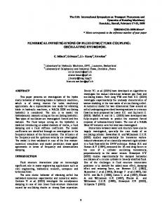
Figure 1. Fabrication of a nanobridge stencil by the edge patterning technique. (a) Formation of a 500 nm-deep Si trench with vertical sidewalls. (b) Conformal deposition of 100 nm-thick low-stress SiN by LPCVD. (c) Patterning of a line-shaped photoresist opening at 90◦ with the trench line. (d) Formation of SiN sidewalls by anisotropic dry etching. (e) Release of the SiN membrane by wet etching of Si in a KOH solution. The configuration for stencil deposition on another substrate is shown in (f).
Cr Si
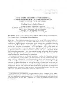
Figure 2. Formation of Cr nanobridge patterns by reverse nanostencil lithography. (a) Growth of 50 nm-thick thermal SiO2 on the Si substrate. (b) Evaporation of 20 nm-thick Cr onto the substrate through the edge-patterned stencil. (c) Formation of primary Cr patterns on the SiO2 layer. (d) Dry and wet etching of SiO2 using Cr patterns as an etch mask. (e) Secondary deposition of 15 nm-thick Cr on the entire substrate. (f) Formation of Cr nanobridge patterns by lift-off in a BHF solution.
many devices over a large area because the thin edge of a cleaved superlattice is used as the template for nanowire structures [10]. In the present work, we propose a new process for fabricating nanobridge patterns by nanostencil lithography. Among many emerging nanolithography techniques [11–15], nanostencil lithography [15] is considered promising with its simple process flow, low cost and little restriction on substrate or pattern materials. In a stencil lithography process, a material is evaporated onto a substrate through a stencil membrane with micro/nanoscaled apertures, by which those patterns are deposited locally onto the substrate. Because the pattern transfer occurs by a simple shadow deposition process, patterns can be formed simultaneously over a large substrate area with little dependence on the pattern layout [16]. In the normal stencil process, an open area in the stencil is transferred as a filled region on the substrate. For obtaining a nanobridge pattern on the substrate, we need a stencil containing a nanoslit connecting two large openings, which should be prepared by either electron beam lithography or focused ion beam (FIB) milling [17, 18]. Because it is impossible to make multiple parallel slits connecting two large apertures, only single-bridge structures can be produced by one deposition step. To overcome these drawbacks, we developed a reverse nanostencil process where a bridge structure in the stencil is transferred also as a bridge pattern on the substrate. For fabricating the nanobridge stencil, we used a new edge patterning technique where many identical nanobridges can be formed simultaneously by a conventional photolithography and dry etching process. By combining those two techniques, we could successfully fabricate 85 nm-wide parallel Cr nanobridge patterns on a Si substrate without the need for advanced lithography techniques for fabricating the nanostencil.
2. Experimental details 2.1. Fabrication of the nanobridge stencil by an edge patterning technique On the front side of a 380 µm-thick double-side polished Si wafer, shallow trenches with vertical sidewalls were formed by the photolithography and anisotropic dry etching process (figure 1(a)). The width and depth of the trenches were 2 µm and 500 nm, respectively. Then, a 100 nm-thick conformal layer of low-stress silicon nitride (SiN) was deposited over the whole surface by low-pressure chemical vapour deposition (LPCVD) (figure 1(b)). After forming line-shaped resist openings by photolithography so that those lines crossed the preformed trench lines at 90◦ (figure 1(c)), the SiN on the top surfaces of the substrate was dry etched using the resist pattern as an etch mask. Because the dry etching process of SiN was anisotropic, the SiN layer still remained along the trench sidewalls after removing the photoresist (figure 1(d)). After defining the backside windows for KOH etching and removing the bulk Si by anisotropic wet etching in a KOH solution, a SiN membrane containing parallel nanobridge structures was finally obtained (figure 1(e)). This SiN membrane was used as a nanostencil on another substrate in the following process (figure 1(f)). 2.2. Formation of parallel nanobridge patterns by a reverse nanostencil process A Si wafer was oxidized to have a 50 nm-thick SiO2 layer, as a substrate for the reverse patterning process (figure 2(a)). By evaporating 20 nm of Cr onto the substrate through the nanobridge stencil fabricated by the edge patterning technique 2
Nanotechnology 18 (2007) 044002
C W Park et al
sidewalls of a trench. Because all nanobridges within a stencil are formed simultaneously, the number of nanobridges can be multiplied simply by increasing the number of trenches, with no need for any additional steps. In addition, as the width of nanobridges is determined by the thickness of a membrane layer grown by the CVD process, a bridge as narrow as a few tens of nanometres is feasible by using a conventional photolithography and anisotropic dry etching process. When using other advanced lithography techniques, such as electron beam lithography or FIB milling [17, 18], the total process time increases with the number of bridges because patterns are produced in a serial manner. In figure 3, the actual width of a nanobridge (∼115 nm) was slightly larger than the thickness of the SiN layer (∼100 nm), which is thought to be because the trench sidewall was not exactly vertical. Figures 4(a)–(c) show the evolution of a doublenanobridge structure during the reverse nanostencil process using a 100 nm-thick stencil. A nanobridge in the stencil (figure 4(a)) was first transferred as a nanogap structure by the normal stencil process (figure 4(b)) and then reversed to the final nanobridge pattern on the Si substrate (figure 4(c)). As indicated in figures 4(a) and (b), the width of the nanogap in the primary Cr pattern (∼85 nm) was narrower than the initial width of the stencil nanobridge (∼115 nm), which was caused by the pattern blurring during the stencil deposition [19, 20]. The blurring effect, which is induced by a non-zero size of the evaporation source and a gap between the stencil and substrate, makes the deposited pattern larger than the original aperture size [19, 20]. In the normal stencil process, we need to minimize the blurring to keep the width of a bridge pattern as small as possible, close to that of the original slit in the stencil. In the reverse process, although it still remains as a challenge to control the amount of blurring and obtain a high uniformity over a large substrate area [20, 21], we can utilize the blurring for reducing the pattern width even further because a bridge structure of the stencil is first transferred as a narrower gap on the oxide layer. During the following steps transferring the
Top view
SiN 115nm
hole
400nm Figure 3. Scanning electron microscopy (SEM) image of nanobridge structures in a 100 nm-thick SiN stencil produced by the edge patterning technique.
as described earlier (figure 2(b)), the primary Cr pattern was formed on the oxide layer (figure 2(c)). Using the Cr pattern as an etch mask, the oxide layer was dry etched and then slightly wet etched so that an undercut of ∼50 nm was formed along the periphery of the pattern (figure 2(d)). In the next step, 15 nm of Cr was evaporated again over the entire substrate area, whereby the deposition of Cr on the oxide sidewall was prevented by the overhanging structure of the primary Cr layer (figure 2(e)). Finally, the Cr/SiO2 layer was lifted off in a 7:1 buffered HF (BHF) solution, leading to the formation of reversed Cr nanobridge patterns on the Si substrate (figure 2(f)).
3. Results and discussion Figure 3 shows a pair of nanobridges in a 100 nm-thick SiN stencil, which has been fabricated by the edge patterning technique. In the edge patterning process, nanobridges are always produced as a pair because they are formed along the
(a)
SiN
(c)
(b) Si
hole
Cr/SiO2
400nm
400nm
400nm
Si
Cr/SiO2 115nm
85nm
SiN
Si
Cr
85nm
Si
Cr Cr/SiO2
200nm
200nm
200nm
Figure 4. The evolution of a double-nanobridge structure during the reverse nanostencil process. (a) Initial nanobridges in the SiN stencil, (b) the Cr nanogap patterns after stencil deposition and SiO2 etching, and (c) the finally reversed Cr nanobridge patterns.
3
Nanotechnology 18 (2007) 044002
C W Park et al
SiN
SiN
Si
Si
(c)
(d)
SiN
SiN
Si
Si
(e)
of the stencil membrane could be suppressed very effectively by adding some corrugated support structures into the membrane [20]. In the edge-patterned stencil, each pair of bridges is always accompanied by one corrugation, which comes from the trench used for forming vertical sidewalls. As a result, for the same membrane thickness, the edge-patterned stencil would be more stable than the planar stencil patterned by electron beam lithography or FIB milling. However, in the edge patterning process, the membrane thickness is fixed at the same value as the width of the nanobridges. If the target width of nanobridges is too small, it is difficult to keep such a thin membrane mechanically stable over a large area. In that case, we can modify the edge patterning process as shown in figure 5. In this process, a thick SiN layer is first deposited on the entire substrate before forming trenches (figure 5(a)), so that a sufficient thickness can be maintained over most of the membrane area except the small trench regions (figure 5(e)). The width of the nanobridges is determined by the thickness of the second SiN layer, which is deposited after forming trenches (figures 5(c), (d)). As we have discussed, the edge patterning technique is a high-throughput and low-cost process suitable for fabricating a stencil containing a large number of parallel nanobridge structures. If combined with the normal stencil process, a multiple-bridge stencil can also be used to produce arrays of nanofluidic channels, which is of great interest for chemical or biological applications [23, 24].
(b)
(a)
SiN sidewall
nanobridge
SiN thick membrane
Figure 5. Fabrication of a reinforced stencil with very narrow nanobridges. (a) Deposition of a thick SiN layer on the Si substrate. (b) Formation of a Si trench with vertical sidewalls. (c) Secondary deposition of a thin SiN layer. (d) Formation of SiN sidewalls by anisotropic dry etching. (e) Release of SiN nanobridge structures supported by a thicker membrane area.
gap to the reversed bridge pattern there was little change in the pattern size (figures 4(b), (c)). The blurring was also beneficial for obtaining smoother pattern boundaries. Due to the inherent roughness of trench sidewalls formed by the photolithography and dry etching process, the line-edge roughness of the stencil nanobridges was observed to be ∼20 nm (figure 4(a)), which is quite a bit larger than those reported for the electron beam lithography patterns (a few nanometres) [8, 22]. However, as the blurring concealed some small irregularities during the stencil deposition, the roughness of the pattern boundaries was reduced to ∼10 nm in the final structure (figure 4(c)). In order to obtain nanobridge patterns by the normal stencil process, we have to use a stencil containing nanoslits each of which connects two large openings. For forming nanoslits on the stencil membrane, it is necessary to use electron beam lithography or FIB milling [17, 18]. Therefore, it would be much more costly and take a longer time to prepare a stencil, especially for massive fabrication over a large area. In addition, as it is impossible to have more then one slit connecting two certain openings within a stencil, an array of parallel bridge patterns cannot be produced by one deposition step in the normal stencil process. In the reverse stencil process, however, we can form many parallel nanobridge patterns on the substrate using a stencil with parallel nanobridge structures as well. By fabricating the nanobridge stencil by the edge patterning technique without using advanced lithography tools, the overall process can be more cost-effective than using the normal stencil process. Furthermore, edge-patterned stencils are expected to be mechanically more stable than those produced by other lithography techniques. During the stencil deposition, the pattern material accumulated on the stencil induces some residual stresses within the membrane, which leads to a substantial deformation of the membrane [20]. Recently, it was demonstrated that such a deposition-induced deformation
4. Conclusions We have developed a new edge patterning technique for fabricating a stencil with parallel nanobridge structures, where those nanobridges can be formed simultaneously by the conventional photolithography and dry etching process. By reversing the primary pattern formed by deposition through the edge-patterned stencil, we could finally obtain 85 nmwide parallel Cr nanobridge patterns on the Si substrate. With no need for advanced lithography techniques in preparing the nanobridge stencil, the combination of the edge patterning and reverse nanostencil process provides a highly cost-effective tool for the massive fabrication of parallel nanobridge arrays at the 100 nm scale.
Acknowledgments We are pleased to acknowledge the EPFL Center of MicroNano-Technology (CMI) and its entire staff as well as our colleagues at the Microsystems Laboratory for their very valuable discussions and help. This project is partially funded by the European Commission and OFES within the project NaPa (contract no NMP3-CT-2003-500120) and by the Swiss National Science Foundation project NANO-IC (contract no 200021-101847). This work was also supported by the Korea Research Foundation Grant (KRF-2005-214D00129).
References [1] Hisamoto D, Lee W C, Kedzierski J, Takeuchi H, Asano K, Kuo C, Anderson E, King T J, Boker J and Hu C 2000 IEEE Trans. Electron Devices 47 2320 [2] Lemme M et al 2003 Microelectron. Eng. 67/68 810
4
Nanotechnology 18 (2007) 044002
C W Park et al
[3] Hu S F, Wu Y C, Sung C L, Chang C Y and Huang T Y 2004 IEEE Trans. Nanotechnol. 3 93 [4] Takahashi Y, Namatsu H, Kurihara K, Iwadate K, Nagase M and Murase K 1996 IEEE Trans. Electron Devices 43 1213 [5] Patolsky F and Lieber C M 2005 Mater. Today 8 20 [6] Wanekaya A K, Chen W, Myung N V and Mulchandani A 2006 Electroanalysis 18 533 [7] Li Z, Rajendran B, Kamins T I, Li X, Chen Y and Williams R S 2005 Appl. Phys. A 80 1257 [8] Namatsu H, Watanabe Y, Yamazaki K, Yamaguchi T, Nagase M, Ono Y, Fujiwara A and Horiguchi S 2003 J. Vac. Sci. Technol. B 21 1 [9] Chen Y, Jung G Y, Ohlberg D A A, Li X, Stewart D R, Jeppesen J O, Nielsen K A, Stoddart J F and Williams R S 2003 Nanotechnology 14 462 [10] Beckman R A, Johnston-Halperin E, Melosh N A, Luo Y, Green J E and Heath J R 2004 J. Appl. Phys. 96 5921 [11] Guo L J 2004 J. Phys. D: Appl. Phys. 37 R123 [12] Piner R D, Zhu J, Xu F, Hong S and Mirkin C A 1999 Science 283 661 [13] Wilbur J L, Kumar A, Biebuyck H A, Kim E and Whitesides G M 1996 Nanotechnology 7 452 [14] Meister A, Liley M, Brugger J, Pugin R and Heinzelmann H 2004 Appl. Phys. Lett. 85 6260
[15] Brugger J, Berenschot J W, Kuiper S, Nijdam W, Otter B and Elwenspoek M 2000 Microelectron. Eng. 53 403 [16] Van den Boogaart M A F, Kim G M, Pellens R, Van den Heuvel J P and Brugger J 2004 J. Vac. Sci. Technol. B 22 3174 [17] Deshmukh M M, Ralph D C, Thomas M and Silcox J 1999 Appl. Phys. Lett. 75 1631 [18] Kim G M, Kawai S, Nagashio M, Kawakatsu H and Brugger J 2004 J. Vac. Sci. Technol. B 22 1658 [19] Racz Z, He J, Srinivasan S, Zhao W, Seabaugh A, Han K, Ruchhoeft P and Wolfe J 2004 J. Vac. Sci. Technol. B 22 74 [20] Van den Boogaart M A F, Lishchynska M, Doeswijk L M, Greer J C and Brugger J 2006 Sensors Actuators A 130/131 568 [21] Takano N, Doeswijk L M, Van den Boogaart M A F, Auerswald J, Knapp H F, Dubochet O, Hessler T and Brugger J 2006 J. Micromech. Microeng. 16 1606 [22] Namatsu H, Takahashi Y, Yamazaki K, Yamaguchi T, Nagase M and Kurihara K 1998 J. Vac. Sci. Technol. B 16 69 [23] Hibara A, Saito T, Kim H B, Tokeshi M, Ooi T, Nakao M and Kitamori T 2002 Anal. Chem. 74 6170 [24] Wang K, Yue S, Wang L, Jin A, Gu C, Wang P, Wang H, Xu X, Wang Y and Niu H 2006 IEE Proc. Nanobiotechnol. 153 11
5