Oct 18, 2001 - implemented in a dedicated PCI interface circuit from AMCC [4]. .... [4] Applied Micro Circuit Corporation, âS5935 PCI Product Data Bookâ,.
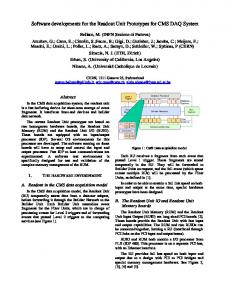
EUROPEAN ORGANIZATION FOR NUCLEAR RESEARCH European Laboratory for Particle Physics
Publication ALICE reference number
ALICE-PUB-2001-47 version 1.0 Institute reference number Date of last change
2001-10-18
PCI Based Read-out Receiver Card in the ALICE DAQ System
Authors:
W. Carena, P. Csató, E. Dénes, R. Divià, K. Schossmaier, C. Soós, J. Sulyán, A. Vascotto, P. Vande Vyvre for the ALICE Collaboration
PCI Based Read-out Receiver Card in the ALICE DAQ System W. Carena (1), P. Csat´o (2), E. D´enes (2), R. Divi`a (1), K. Schossmaier (1), C. So´os (1) , J. Suly´an (2), A. Vascotto (1), P. Vande Vyvre (1) for the ALICE Collaboration CERN EP-AID (1) , CH-1211 Geneva 23, Switzerland KFKI-RMKI (2) , H-1121 Budapest, Hungary Abstract The Detector Data Link (DDL) is the high-speed optical link for the ALICE experiment. This link shall transfer the data coming from the detectors at 100 MB/s rate. The main components of the link have been developed: the destination Interface Unit (DIU), the Source Interface Unit (SIU) and the Read-out Receiver Card (RORC). The first RORC version is based on the VME bus. The performance tests show that the maximum VME bandwidth could be reached. Meanwhile the PCI bus became very popular and is used in many platforms. The development of a PCI-based version has been started. The document describes the prototype version in three sections. An overview explains the main purpose of the card: to provide an interface between the DDL and the PCI bus. Acting as a 32bit/33MHz PCI master the card is able to write or read directly to or from the system memory from or to the DDL, respectively. Beside these functions the card can also be used as an autonomous data generator. The card has been designed to be well adapted to applications, which require small software overhead such the high-speed data acquisition systems. The implementation of the firmware will be presented. For the logic design we are using VHDL and schematic draw. Software library routines were written in C and are available on Linux OS. The results of performance measurements will be available to allow the comparison between the VME-RORC and PCI-RORC. In the conclusion the future plans and the idea of the improved (64bit/66MHz) PCI-RORC will be shown.
1
Overview
The Detector Data Link (DDL) is an integral part of the ALICE [1] data acquisition system (DAQ). The DDL shall provide duplex data transfer between the detectors and Local Data Concentrators (LDC) at up to 100 MB/s speed. The DDL consists of three main parts, the Source Interface Unit (SIU), the optical medium and the Destination Interface Unit (DIU). This naming convention is based on the fact that the main data flow is coming from the detectors. Accordingly the SIU card is sitting on the detector side connected to the Front-end Electronics Cards (FEE) and the DIU is plugged in the LDC computers. A Read-out Receiver Card (RORC) shall provide the interface between the Detector Data Link (DDL) and the LDCs. The DIU interfaces are specified by [2]. Forward channel Front-end Electronics (FEIC)
Source Interface Unit (SIU)
Destination Interface Unit (DIU) Backward channel
Read-out Receiver Card (RORC)
DDL hardware = Source Interface Unit + Physical Medium + Destination Interface Unit
Figure 1: The Detector Data Link The connection between the LDC and the RORC depends on the local I/O bus employed in the computer. Few years ago the PCI local bus was not as widespread as today and an evolution of the VME bus toward higher performance was expected. Therefore the first version of the RORC card was developed for VME systems [3]. This card was used for testing the prototype version of the DDL components as well as to measure the DDL performance connected to the VME bus. The results of those measurements show that the DDL transfer speed was only limited by the VME maximum speed. It was also clear that the VME based RORC card (VME-RORC) was expensive and complex. At present, the PCI local bus exists in any computer and provides enough bandwidth for the DDL. The theoretical speed is 132 MB/s with the 32bit/33MHz version and 528 MB/s with the 64bit/66MHz version and the expected evolution of the VME bus toward higher performance has not materialized.
2
Development
The development was split into two phases. The first version of the PCI based RORC card was defined as 32bit/33MHz PCI master card. To reduce the complexity of the
board, its cost and development time it was decided not to use on board memory. The data shall be transferred directly into the memory of the LDC. Since the card can operate as PCI master the software will only have to allocate enough space in the memory of the computer to let the RORC move the data to the destination. This will reduce the latency and the software intervention, so the DAQ software will be able to make better use of the PCI bus. The required bus functions are implemented in a dedicated PCI interface circuit from AMCC [4]. The custom logic functions for the DIU interface are realized in a Programmable Logic Device (PLD) from ALTERA. The firmware is divided into three parts according to functions they provide (Figure 2): • The add-on logic section handles the signals between the PLD and the PCI bridge. It also manages the add-on logic bus, performs the arbiter function for the different firmware parts and reads the mailboxes. • The internal control and command manager receives the commands and controls the firmware to carry out the required actions. This part contains the write and read DMA engines and the memory manager as well. • The DIU interface, is dealing with the DIU. It contains FIFOs to store the data and a pattern generator that can be used for test purposes.
PCI to AOL FIFO
PCI AOL to PCI FIFO
AOL interface
IMB
Internal Control
DIU interface
Read DMA controller
Transmitter FIFO
Memory manager and command interpreter
Write DMA controller
Pattern generator
DIU
Receiver FIFO
OMB
Figure 2: Architecture of the pRORC The control of the card is done by commands. A command may have parameters as well. The commands are passed through the incoming mailboxes of the PCI interface circuit. There are four incoming mailboxes in the device. Each mailbox is 32-bit wide. The add-on logic is notified if there is a new command waiting in the
mailboxes. This is done by a hardware interrupt that is raised if one predefined byte of the incoming mailboxes becomes full. The response of the RORC is sent back through the outgoing mailboxes. Since the PCI interrupt should be avoided there is no particular notification to the software about the state of the outgoing mailboxes. However, the RORC shall not generate any response without a request from the software. The DDL is using the same mechanism for the status and error reporting. The add-on logic keeps track of the outgoing mailboxes to avoid overwriting any data, which is waiting for the software. The PCI bridge has a 32-bit bi-directional add-on local bus with separate address lines. The add-on logic can use this bus to access the registers, mailboxes and FIFO channels of the bridge. There are different parts of the firmware competing for the bus access. The add-on logic contains a bus manager, which plays the role of the arbiter. The arbitration is based on a predefined priority scheme and performed by internal request and grant signals. According to this scheme the command transfer has the highest priority, which ensure the controllability of the RORC even during DMA transfer. The DDL interface makes the connection between the DIU and other parts of the firmware like the DMA channels. It contains FIFOs on both the transmit and the receiving side in order to separate the different clock domains and to balance the data transfer speed on the link. There are two FIFOs in the receiver and one FIFO and a command register in the transmitter. The data and status in the receiver may come from the DDL or from the transmitter via an internal loop-back. This loop-back can be used for self-test. The input of the transmit FIFO can also be connected to two different sources. It is either the output of the read DMA channel or the output of the internal test pattern generator. The test pattern generator is able to produce data blocks with different lengths and patterns. The cycle number is selectable or it can be set to infinite. The internal control and command manager receives the commands from the add-on logic. Depending on the destination the command will be interpreted or sent over the link via the DDL interface. The partial memory management is carried out by this part of the firmware. It contains the DMA engines, which control the data transfer to and from the PC memory. The write DMA (WDMA) is writing to the PC memory while the read DMA (RDMA) is reading from the PC memory. The DMA engines are using the FIFOs implemented in the PCI bridge to do the transfer. The PCI bridge contains primary registers to control the data transfer. When the bridge operates as PCI master these registers are accessible from the add-on logic. One register defines the base address of the DMA transfer and the transfer count is stored in other register. There are two sets of such registers for read and write DMA. The applied memory management supports the so-called scattered memory model. This will be used in the next version of the Data Acquisition and Test Environment (DATE) software [5]. In this model the data blocks are transferred to different memory locations in the PC memory. The software running on the machine is
maintaining a list of free memory pages. In this context page means a buffer of a certain size in the PC memory. To initiate the WDMA the RORC has to know the base address and size of such a memory page. The software shall provide the RORC with this information, so that it can accomplish the transfer. The RORC stores this information in the so-called Free FIFO. Each entry of the Free FIFO consists of three fields containing the base address, the page size and the Ready FIFO index. The latter requires explanation. The hardware has to report the software about the readiness of a memory page. This will happen in two cases, when the page boundary is reached during the DMA or when the block finishes, which is indicated by a status word generated by the DDL. In both case the firmware will close the given page by sending two words to a location in the PC memory. The address of this location is defined by the Ready FIFO index and the Ready FIFO base address. The first word contains the number of words transferred to that memory page. The second word contains zero if the block stretches over the page boundary or the DTSTW status word in case of the block finished. Using this mechanism the software can detect the end of a DMA cycle by simply checking the Ready FIFO in the host memory. (Figure 3) Free FIFO (128 entry)
BA
BL
IDX
Data buffer RFBA Ready FIFO
IDX
BA - Base Address BL - Block Length IDX - Ready FIFO Entry Index RFBA - Ready FIFO Base Address
Figure 3: Memory management
3
Performance test
Since the DDL is ready to provide 100 MB/s bandwidth on the forward channel it is important to know the performance of the RORC card. With the VME based card the measurements showed that the transfer speed is limited by the read-out system. The measured speed was less than 40 MB/s. In order to evaluate the transfer speed using the PCI local bus test firmware and software were developed. The test firmware contains a simple DMA engine and a pattern generator. The
pattern generator generates data blocks with different lengths. The DMA always goes to the same location in the memory. At the end of every block a counter is incremented and then transferred to the host memory (Figure 4). From time to time the software checks this memory location and calculates the transfer speed. The most important signals, which control the DMA, are placed on logic analyzer connectors, so that they can be monitored during the operation. These signals represent well the traffic on the PCI. Base address Block counter
Base address + 4
Data buffer
Base address + 4(n+1)
Figure 4: pRORC performance test 1
DMA speed [MB/s]
In the first test the performance measured in stand-alone operation. There was not any other user process running on the computer. The computer had single processor and the operating system was Linux with 2.2.x kernel. The DMA speed was measured using different block sizes to find out the variation of the speed versus the block size. The result of the test is shown in Figure 5. 140 120 100 80 60 40 20 40
400
4K
40K
400K
2M
4M
6M
Data length [Byte]
Figure 5: DMA speed vs. block size (stand-alone operation) In the second test a more realistic environment was set up. The host computer had two Intel Pentium III processors running at 400 MHz. The installed Linux kernel version was 2.2.x. In order to increase the traffic on the PCI bus a Gigabit Ethernet network interface card was also installed. Beside the test software two
other processes was using the PC resources. A benchmarking tool, called stream l was doing intensive memory operations in order to emulate a process, which would perform data processing in the LDC. Network traffic was generated by iperf. In the last scenario the DATE software consisted of the typical LDC components, like read-out and recorder. The performance of the different processes were measured as well as the combined performance. The DMA size was constant (400 KByte) during the measurement. During the test the DMA speed, the available memory and network bandwidth were measured. The usage of the CPUs was also monitored during the test in order to see the remaining resources for other applications running on the LDCs, like software components of the High Level Trigger (HLT) system. The results are summarized in Figure 6. Scenario
DMA [MB/s]
1
125
-
-
pRORC DMA (0%)
2
-
360
-
stream_l (100%)
3
-
-
40
4
113
310
-
5
80
-
21
6
80
180-210
19-20
Memory Network [MB/s] [MB/s]
Components’ CPU usage
iperf (100%) pRORC DMA(0%) + stream_l(100%) pRORC DMA(0%) + iperf(66%) pRORC DMA(0%) + DATE(66%) + stream_l(100%)
Figure 6: Performance of the LDC components
4
Conclusions and Future Work
The first version of the PCI based Read-out Receiver Card for 32-bit 33MHz PCI was developed. This card is a functional replacement of the VME based RORC and it supersedes the old design in terms of performance. The hardware is rather simple and cheap. The firmware connects the DDL to the LDC computer via DMA channels. The performance tests show that DMA bandwidth allows the DDL to operate at the maximum speed. The software library was developed to provide interface for the read-out software. The next version of the RORC will be based on the 64bit/66MHz PCI. The PCI interface functions will be realized in the PLD by using IP core. Beside the data flow operation the card shall provide data processing functions for the HLT
system. These functions require on-board memory too. The option of an integrated RORC-DIU card will be investigated as well.
References [1] ALICE Collaboration, “ALICE - Technical Proposal for A Large Ion Collider Experiment at the CERN LHC”, CERN/LHCC 1995-71, December 1995. [2] G. Rubin, P.V. Vyvre, “ALICE Detector Data Link (DDL) - Interface Control Document”, ALICE Internal Note, INT-96-43. [3] G. Rubin, J. Suly´an, “The Read-out Receiver Card (RORC) Hardware User’s Guide”, ALICE Internal Note, INT-97-14. [4] Applied Micro Circuit Corporation, “S5935 PCI Product Data Book”, http://www.amcc.com. [5] ALICE Data Acquisition group (ALICE/DAQ), private communication