Connecting TCAD To Tapeout
A Journal for Process and Device Engineers
Pending Issues in the Modeling of Concentrator Solar Cells C. Algora, M. Baudrit, I. Rey-Stolle, D. Martín, R. Peña, B. Galiana and J. R. González Instituto de Energía Solar – E.T.S.I. Telecomunicación – Universidad Politécnica de Madrid Avda. Complutense 38; 28040 Madrid – SPAIN Phone: 34-913367232; Fax: 34-915446341; E-mail:
[email protected]
This article, published in the Proceedings of the 19th European Photovoltaic Solar Energy Conference, Paris, 2004, presents the ability of ATLAS-Luminous3D to
incidence of light onto the solar cell is a common practice in characterisation. Obviously, this type of procedures have had such a great influence on the field of simulation and optimisation, that in fact, the majority of simulation results have assumed the AM1.5D spectrum, normal incidence of light, etc. However, a good solar cell at these “standard” conditions could become in an average solar cell when operates inside an optical concentrator.
simulate heterostructure Solar Cell
Abstract The modelling of concentrator solar cells for real conditions of operation inside optical concentrators is a subject almost untreated. Consequently, this work highlights the main specific situations that should be included in a realistic modelling. The results of a 2-D modelling applied to the case of a 1000 sun GaAs concentrator solar cell inside a TIR-R concentrator are presented. The necessity of going towards a 3-D modelling is also stated. This task is being carried out now at IES-UPM. Keywords: concentrator cells, modelling, III-V semiconductors.
Accordingly, it is necessary to detect the pending issues in the modelling of concentrator solar cells when considering the situations appearing in their real operation. In our opinion, the most influencing ones are: • Different illumination spectra from the standard ones, as a consequence of the pass of light through a given optics. • Inhomogeneous illumination distribution on the solar cell because of the focusing of light. • Light impinging the cell within a cone, as a consequence of the different areas of the optics and solar cell.
1. Introduction In the last years, a great activity is being carried out in Europe, United States and Japan in order to achieve commercial PV modules for terrestrial applications based on concentrator III-V solar cells operating at 200-1000 suns [1, 2, 3]. This activity, which is in the search of a real breakthrough, is requiring very accurate models for concentrator solar cells that conduct to the highest efficiency of PV modules. In order to increase the performance of such concentrator solar cells, a modeling as accurate as possible is necessary to guide the technological approaches. Concentration operation imposes several conditions that should be theoretically assessed in order to achieve realistic results. This is, a model considering real operation conditions as it is proposed in [4].
• Chromatic aberration. • Temperature gradients. At the horizontal plane, they appear as a consequence of the inhomogeneous illumination. At the vertical plane, as a consequence of the different light absorption at the different junctions in a tandem cell. Continued on page 2 ...
INSIDE Process and Device Simulation of Field Emission Microtrides ........................................................ 6 Simulating Selective and Non-Selective Epitaxy Over Oxide Isolated Regions Using Athena ................................... 7
However, standard procedures for characterizing concentrator cells are usually far away from reality. For example, the use of the AM1.5D spectrum with normal
Volume 15, Number 2, February 2005 February 2005
Calendar of Events ................................................................. 9 Hints, Tips, and Solutions ....................................................10
Page 1
The Simulation Standard
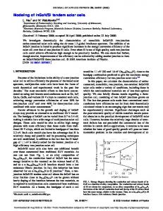
Figure 1. Definitions of 1-D, 2-D and 3-D modeling by using as example a concentrator p/n GaAs solar cell.
Thereby in connection with the consideration of these new issues in the modelling, a new calculation strategy should be applied. Effectively, the aforementioned pending issues have an inhomogeneous distribution in the horizontal or in the transversal plane of the solar cell. Therefore, an evolution from the previous onedimensional (1-D) models towards a two-dimensional (2- D) or three-dimensional (3-D) model should be undertaken.
the series resistance as a lumped parameter to take into account the horizontal variation imposed by the front contact geometry. Finally, a 3-D model accounts for variations in the three directions (as in figure 1, right). This situation applies to many solar cells having their front metal grid with variation in more than one direction (like the circular ones). But in addition to the characteristics of a given solar cell that recommend a 2-D or 3-D modelling, the external conditions can definitively force a 3-D analysis. This is the case, for example, of a solar cell illuminated with a non-uniform beam from a concentrator.
2. Definitions for 1-D, 2-D and 3-D Modeling When simulating semiconductor devices, a common rule for designing what is a 1-D, 2-D and 3-D model is that shown in Figure 1.
Therefore, any concentrator solar cell operating under real conditions should be analyzed with a 3-D model. One the main problems for computing a concentrator solar cell with a 3-D model is the large size of the solar cell. All the 3-D electronic device simulation software tools are conceived for microelectronics. Therefore, when such programs are applied to solar cells their calculation capabilities are not enough for a complete 3-D analysis. In fact, as it is described in [5], some attempts of using such programs for solar cells have been restricted for 2-D purposes.
In a pure 1-D model, the whole structure varies only in one direction (as in Figure 1, left). This situation corresponds to a solar cell with a front metal covering its whole surface. Therefore, no pure 1-D model can simulate any solar cell! However, many people use 1-D models because they analyse the semiconductor structure without the consideration of the contact effects. A 2-D model accounts for variations in two directions (as in figure 1, centre). This situation applies to any solar cell because there is a vertical variation due to the different semiconductor layers plus a horizontal variation due to the metal fingers of the front contact. In order to simplify the physic-mathematic treatment, many people use a 1-D model for the semiconductor equations while including
The Simulation Standard
A very interesting approach for avoiding this limitation and to analyze concentrator solar cells by a 3- D model with distributed parameters can be seen in [6].
Page 2
February 2005
3. Case of Study: 1000 SUN GaAs Solar Cell Inside a TIR-R Concentrator
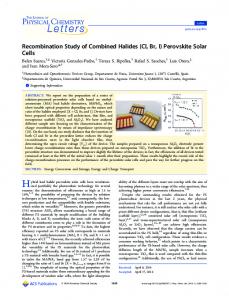
In addition, even for the small size of the simulated solar cell, about 14,000 nodes with a calculation time of about 90 minutes are required for one half of the cell (see Figure 2). Therefore, an optimization of our computing procedures should be carried out for the future 3-D modelling. A draft consideration of the 3-D analysis shows that about 350,000 nodes and about 10 hours will be required for simulating a quarter of the cell (0.6 x 0.6 mm), what is enough considering its symmetry.
In order to show the effects of the pending issues described in the Introduction, it is necessary to choose a given case. We have chosen the case of a 1000 sun GaAs solar cell inside a TIR-R concentrator for the following reasons: • The 1000 sun GaAs solar cell has an area of 1 mm2, following the patent described in [7]. Therefore, its size is much closer to those of microelectronic devices successfully analyzed with the commercial 3-D electronic device simulation programs.
4 Which Spectrum? In the last years, the classical AM1.5D spectrum as defined by ASTM 891-87 has been questioned as being a good reference for concentrator solar cell characterization [11] and consequently, for its simulation and optimization. Several works proposed the AM1.5G as the most appropriate spectrum while others stated a redefinition of the AM1.5D with a lower aerosol optical depth (low AOD).
• The 1000 sun GaAs solar cell plus the TIR-R concentrator are being developed in order to achieve a commercial product [1]. • The combination of such solar cell plus the TIR-R concentrator is well known for us so, all the required data for the analysis are available.
However, the influence in the final performance of the solar cell when choosing one or other standard spectrum is negligible in comparison with the variation in the spectrum produced by the spectral transmission of the optical concentrator. As Figure 3 shows, for wavelengths lower than 900 nm (close to the cut-off wavelength of GaAs), the transmission variation of TIR-R is almost negligible. Nevertheless, for wavelengths higher than 1300 nm the spectral transmission variation becomes important being much more restrictive than the consideration of one or another standard solar spectrum. Such a spectral transmission should be carefully considered when multijunction cells are modelled and optimised.
The TIR-R concentrator exhibits very interesting characteristics like concentrations higher than 1000 suns, acceptance angle: 1.3º (for 90% relative transmission), aspect ratio < 0.3, total planarity of the front surface etc. [8]. Many of its optical properties required in the present analysis can be found in [9]. We have used the ATLAS simulation software from Silvaco [10]. In this paper, we present only 2-D analyses because, as a starting point, the effects of including the pending issues can be clearly shown.
Figure 3. Spectral transmission of the TIR-R concentrator.
5. Non-Uniform Illumination For normal incidence of the sunlight, the TIR-R concentrator produces an irradiance distribution over the 1 mm2 solar cell of about 1000 suns as average with a maximum value of 1850 suns. Figure 2. Cross-section of a half GaAs solar cell (500 microns for the active area plus 100 microns for the bus bar). The mesh for the 2-D calculations is also shown.
February 2005
When the sunlight is tilted within the acceptance angle of the concentrator, the maximum irradiance goes up. Therefore, we have considered here as a representative Page 3
The Simulation Standard
Figure 5. Illumination I-V curve of the concentrator GaAs solar cell when is illuminated with an uniform irradiance of 1000 suns (top curve) and when it is illuminated with the profile of the top of Figure 4 (bottom curve). The front contact parameters are medium quality.
Although here the 2-D simulation contributes to a better understanding of the real operation of the solar cell, the non-uniformity of the light is an excellent example of the need of a 3-D simulation. Effectively, the irradiance profile of Figure 4 is applied only to a portion of the cell while in other regions of the cell a different profile exists. In addition, the number of fingers through the horizontal dimension of the cell (15 in figure 4) also changes across the cell area.
Figure 4. 2-D irradiance profile (in suns) over a complete section of the 1 mm2 solar cell. The integration of such profile produces an average of 1000 suns. The horizontal scale is in mm (top). Photogeneration produced by the top profile over the GaAs solar cell. The vertical dimension of the cell is magnified and takes about 5 microns (bottom).
example of the worst case, the sun placed at 0.8º from normal incidence. In such case, the irradiance distribution on the solar cell is shown in Figure 4 (top).
Therefore, a 3-D modelling of the whole solar cell is required. This requirement is even more important when considering multijunction solar cells in which the current matching of the different junctions is fundamental. This 3-D modelling is being carried out at IES-UPM.
This profile is applied to a complete section of the GaAs solar cell. As Figure 4 (bottom) shows all the elements of the solar cells are included in their proper scale: bus bars at horizontal extremes separated by 15 metal fingers with a thickness of 0.5 microns and a width of 3 microns. The semiconductor structure includes all the layers: cap (n-GaAs), window (n-GaInP), emitter (n- GaAs), base (p-GaAs), BSF (n-GaInP) and GaAs substrate (although in Figure 4 the substrate is not shown due to the magnification).
6. No Normal Incidence of Light Because of the large area of the concentrator compared to the solar cell, the light impinges on the cell in the shape of an inverted cone, pyramid, etc (depending on the type of optics). The treatment of the performance of a solar cell operating under wide-angle cones of light was stated in [12].
The photogeneration in figure 4 is shown in a grey scale from 1023 (black) to 1025 e-h pairs/cm3/s (white). As can be seen, the depth of the photogeneration reproduces the shape of the irradiance profile. There are many magnitudes whose variation across the solar cell section could be shown. Anyway, the most important implication of the non-uniformity of light is its effect in the whole performance of cell, that is, the illumination IV curve that is shown in Figure 5.
In [13], the scarce influence of the wide-angle cone of light on the semiconductor structure was analysed. The reason for this is because the critical angle (that is the refracted angle when the incident ray is parallel to the surface) of GaAs is only about 17º so, no big variations of the light path inside the semiconductor are expected. Therefore, in the worst case the light would enter the first semiconductor with an angle of 17º (with regard to the normal) while the angle would be almost 0º for the subsequent layers. So, even a multijunction cell would not be affected in its semiconductor structure optimization.
As can be seen, the non-uniform illumination increases the deleterious effect (voltage drop) of the series resistance. The main losses are in the grid, front contact and emitter. Consequently, a proper design of the solar cell for real condition operation should reconsider the front grid parameters in order to minimize this effect. The Simulation Standard
Page 4
February 2005
However, the cone of light does affect the ARCs design because their refraction indexes are much lower than those of III-V semiconductors, so light enters ARCs really tilted. Additionally, geometric considerations of ray tracing should be taken into account like for example overconcentration in the semiconductor regions close to the fingers as consequence of reflection on light in them and photogeneration under the fingers.
Ministry. The Spanish Ministry of Science and Technology has also contributed by means of the research projects with references TIC2002- 01012 and TIC2002-11391-E.
7. Chromatic Aberration
[2] T. Takamoto, T. Agui, K. Kamimura, M. Kaneiwa, M. Imaizumi, S. Matsuda and M. Yamaguchi, Proc. of the 3rd world PV conference 3PL-C2-01 (Osaka, Japan 2003).
References [1]
This effect has not been detected in the TIR-R concentrator but could have a certain importance in other optics like Fresnel lenses.
J. Alonso, V. Díaz , J. Ruiz , E. Perezagua, C. Algora, P. Benítez, J. C. Miñano, A. Luque, R. Heyer, A. Schmidt, H. Franz, W. Preuss, A. Gessenharter and J. C. González, Proc. of the PV in Europe: from PV technology to energy solutions, 530-533. (Rome, Italy 2002).
[3] H.L. Cotal, D.R. Lillington, J.H. Ermer, R.R. King, N.H. Karam, S.R. Kurtz, D.J. Friedman, J.M. Olson, J.S. Ward, A. Duda, K.A. Emery, and T. Moriarty, Proc. of the 28th PVSC 955-960. (Anchorage, Alaska 2000).
8. Summary and Conclusions
[4] C. Algora, “The importance of the very high concentration in thirdgeneration solar cells” Chapter 6 of the book “Next generation Photovoltaics, High efficiency through full spectrum utilization”. Ed. A. Martí and A. Luque (Institute of Physics, 2004).
The modelling of concentrator solar cells for real conditions of operation inside optical concentrators is a subject almost untreated. This is because, in spite of the existence of a very good previous work on the side of solar cell modelling as well as in the optics (independently considered), there are almost no studies that combine both aspects. So, this work considers jointly the performance of the solar cell and the optics as a whole.
[5] C. Algora, Semiconductors 38 (8), 958 (2004). [6] B. Galiana, I. Rey-Stolle, C. Algora, M. Baudrit and I. García, «3D Distributed Model for Concentrator Solar Cells”, Proc. of this Conference. [7] Universidad Politécnica de Madrid, European Patent Application EP 1278248A1 and United States Patent Application US 2002/ 0170592 A1.
Accordingly, the main pending issues in the modelling of concentrator solar cells when considering the situations appearing in their real operation are: different spectra from the standard ones, as a consequence of the pass of light through a given optics (spectral transmission), inhomogeneous illumination of the solar cell because of the focusing of light, light impinging the cell within a wide-angle cone, chromatic aberration, temperature gradients at both the horizontal and vertical plane, etc.
[8] J. L Alvarez, M. Hernández, P. Benítez, J. C. Miñano, Nonimaging Optics: Maximum Efficiency Light Transfer VI, Proc., pp.32- 42, (2001). [9] M. Hernández, P. Benítez, J. C. Miñano, J.L. Alvarez, V. Diaz and J. Alonso, Proc. of 3rd World Conf. Photovoltaic on Solar Energy Conversion 3P-C3-77 (Osaka, Japan, 2003). [10] ATLAS User’s Manual. Device simulation Software. Volumes I and II. Silvaco International (2002). [11] K. Emery, D. Myers and S. Kurtz, Proc. of the 29th IEEE PVSC 840-843. New Orleans (2002). [12] C. Algora and V. Díaz, Prog. Photovolt: Res. Appl. 7, 379-386 (1999).
All these effects (with the exception of temperature gradients) have been included in a 2-D modelling applied to the case of a 1000 sun GaAs concentrator solar cell inside a TIR-R concentrator. For each effect, results in order to increase the efficiency of the cell are derived. Therefore, it is demonstrated that concentrator solar cells should be designed (and manufactured) to match a given optical concentrator (and vice versa). The necessity of going towards a 3-D modelling is also stated. This task is now being carried out at IES-UPM.
[13] C. Algora, V. Díaz and I. Rey-Stolle, Proc. of the 29th IEEE PVSC 848-851, N. Orleans, USA (2002).
Acknowledgements The authors would like to express their gratitude to the members of the Optics Group of the Solar Energy Institute of Madrid for supplying several optical data about the TIR-R concentrator. This paper has been supported by the European Commission under contract SES6-CT-2003-502620 (FULLSPECTRUM project) and also by means of FEDER funds for scientific infrastructure managed in collaboration by Spanish
February 2005
Page 5
The Simulation Standard
Process and Device Simulation of Field Emission Microtrides Introduction One of the most beneficial merits of computer-based experiment using TCAD lies in its capability of a total simulation of the target device. One can consider its novel fabrication process and its device performance at the same time without time consuming and expensive experiments using real wafers. Take field emission microtriodes, for example. They have been studied for various applications such as field emission displays, highpower and high-frequency devices having high-operating temperature and radiation hardness. In order to fabricate the microtriodes, silicon wafer process technology is preferred because it is suitable in forming a sharp cone structure as its field emitter(1).
Process Simulation The electrical performance of the device is very sensitive to the physical configuration of its structure. Precise and stable fabrication
Figure 1. A microtriode fabrication process simulaitons by ATHENA.
processes are necessary. In many cases, compatibility with a conventional CMOS process is also required for the integration of driver circuits around it. One can investigate and optimize desirable process steps using ATHENA process simulator. Figure 1 shows simulated process steps for a microtriode, applying the idea developed for a field emitter array fabrication process(2). Starting from an n-type silicon bare wafer, masking oxide is deposited and patterned, then RIE etching is performed to get a base shape of the field emitter. The first oxidation sharpens the emitter. After forming a silicon nitride cap on it, the second oxidation is performed to complete the grid insulator and to adjust the position of grid electrodes. The nitride cap is removed and grid metal is deposited. The overlying structure on the emitter is removed by lift-off and RIE etching. Figure 2. Current flow lines and potential contours by ATLAS. Continued on page 8...
The Simulation Standard
Page 6
February 2005
Simulating Selective and Non-Selective Epitaxy Over Oxide Isolated Regions Using Athena 1.0 Introduction In certain cases, most notably in modern bipolar and SiGe HBT structures, epitaxial steps are performed after the oxide isolation structures have been already created. Thus the initial surface prior to epitaxy may contain regions of crystalline silicon, polysilicon or insulators, usually silicon dioxide. In the case of LOCOS isolation, the surface is also non-planar. In such epitaxial cases, epitaxy can be divided into two general types: (i) non selective epitaxy (ii) selective epitaxy In the first case, silicon is deposited epitaxially onto any exposed crystalline surface, and polysilicon is deposited onto amorphous regions such as oxide isolation or regions where poly-silicon already exists. In the second case, the use of selective chemistry increases the silicon layer seeding time on non crystalline surfaces to such an extent, that effectively silicon is only deposited epitaxially onto exposed crystalline surfaces.
Figure 1. Structure Prior to Epitaxial Growth.
No polysilicon or amorphous silicon is deposited onto the oxide isolated regions. In this article, the methodology for simulating both these scenarios is described.
2.0 Non Planar LOCOS Structure Example In order to demonstrate the epitaxial capabilities, a standard LOCOS structure is used as the starting substrate, since this presents a surface that is both non planar and contains a combination of crystalline and non crystalline surfaces. The structure prior to epitaxy is a simple LOCOS isolated active region as shown in Figure 1. Following a high temperature anneal to remove the native oxide, a typical ATHENA epitaxy statement would then be as follows: epitaxy time=1 temp=1000 thickness=0.2 divisions=8 c.boron=1e15 SI_TO_POLY
Figure 2. Structure After Non-Selective Epitaxial Growth .
February 2005
Page 7
The Simulation Standard
The key parameter in the ATHENA epitaxy statement that invokes the automated deposition of polysilicon on non crystalline regions of the device is “SI_TO_POLY”. Other parameters such as c.boron=1e15 are simply inserted to emulate the un-intentional doping that occurs during epitaxy. Intentional doping can also be added using the same syntax format. After the ATHENA epitaxy statement above, the structure is now as shown in Figure 2. Simulating selective epitaxy is now very simple because the epitaxial growth on the non crystalline regions is now polysilicon rather than silicon. Thus the simple statement “etch poly all” removes the poly silicon layer over the oxide leaving behind a structure as it would appear if selective epitaxy was used instead. After the etch above, the structure now appears as shown in Figure 3. Figure 3. Structure After Emulating Selective Epitaxial Growth.
...continued from page 6
Device Simulation Once a desirable structure is obtained by ATHENA process simulation, one can transfer it to ATLAS device simulation directly. In some cases, remeshing suitable for device simulation may be needed to obtain a better convergence and that is easily done using an user-friendly interactive meshing tool DevEdit. In order to estimate the electrical characteristics of the emitter, Fowler-Nordheim equation is used. Figure 2 shows electric potential contours and current flow lines at the anode and grid voltages of 800V and 10V respectively. It can be seen that the current flow lines respond very sensitively to slight irregularities in the shape of the structure. The final results of the emitter current vs. anode voltage curves at various grid voltages are shown in Figure 3.
Conclusion
Figure 3. ATLAS simulation results of emitter currents as a function of anode
An field emission microtriode can be simu- voltage for different grid voltages. lated continuously starting from a bare wafer, going through the device structure, to the resultant References I-V curves, using TCAD process and device simulators (1) C.E.Holland, Rosengreen, and C.A.Spindt, IEEE ED., ATHENA and ATLAS. Making good use of TCAD total No.10, 2368(1991). simulations will reduce process development time and (2) H.S.Uh, S.J.Kwon, and J.D.Lee, IEEE EDL., Vol.16, 488(1995). the number of trial experiments. The Simulation Standard
Page 8
Vol.38, No.11,
February 2005
Calendar of Events February 1 2 3 4 5 6 7 DATE - Munich, Germany 8 DATE - Munich, Germany 9 DATE - Munich, Germany 10 DATE - Munich, Germany 11 DATE - Munich, Germany 12 13 14 15 16 17 18 19 20 21 22 23 24 25 26 27 28 29
March 1 2 3 4 5 6 7 8 9 10 11 12 13 14 15 16 17 18 19 20 21 ISQED - San Jose, CA 22 HEART - Tampa, FL ISQED - San Jose, CA 23 HEART - Tampa, FL ISQED - San Jose, CA 24 25 26 27 28 29 30 31
Bulletin Board DATE – Design, Automation, and Test in Europe Come and see Silvaco applications engineers demonstrate complete analog, mixed-signal, and RF IC design solutions. Silvaco supports this integrated design flow with process design kits (PDK) targeted to specific foundry processes.
ISQED International Symposium on Quality Electronic Design Ken Brock, Silvaco’s VP of marketing will participate in the evening panel titled “IP Creation and Use-What roadblocks are ahead or it is just clear and bumpy road?” This panel will debate and discuss the key technology and business issues that could disrupt the basic premises of cell-based design using IP blocks. The panel includes representatives of semiconductor manufacturers, EDA vendors, design managers, and IP providers.
If you would like more information or to register for one of our our workshops, please check our web site at http://www.silvaco.com The Simulation Standard, circulation 18,000 Vol. 15, No. 2, February 2005 is copyrighted by Silvaco International. If you, or someone you know wants a subscription to this free publication, please call (408) 567-1000 (USA), (44) (1483) 401-800 (UK), (81)(45) 820-3000 (Japan), or your nearest Silvaco distributor. The following trademarks and service marks are the property of Silvaco International. Registered Marks:® Virtual Wafer Fab, Silvaco. Trademarks: ™ Simulation Standard, ATHENA, Analog Alliance, Legacy, Manufacturing Tools, Automation Tools, SFLM, VICTORY, Ranger3D Nomad, VYPER, SmartSpice, PSTATS, UTMOST IV, Measure, DISCOVERY, MERCURY, Optolith,TCAD Driven CAD, TonyPlot3D, RESILIENCE, Flash, ATHENA Interpreter, Interactive Tools, DeckBuild, DevEdit, ANALOG EXPRESS, CELEBRITY, SSuprem3, ATLAS, ATLAS Interpreter, Luminous2D/3D, MC Implant, S-Pisces, TonyPlot, FastLargeSignal, SmartStats, Ferro, DevEdit3D, Interpreter, Quantum2D/3D, SDDL, Circuit Optimizer, MaskViews, TFT2D/3D, Radiant, SSuprem4, Elite, FastBlaze, Mocasim, Silicides, MC Depo/Etch, FastNoise, Clarity, Blaze/Blaze3D, Device3D, Frontier, TwinSim, MixedMode2D/3D, VCSELS, Maverick, Envoy, Giga2D/3D, FastGiga, Guardian, Scout, FastMixedMode, Laser, Dragon, Expert, Spirit, Beacon, Savage, Harm, Zenith, Vision, Scholar, SN, UTMOST, UTMOST II, UTMOST III, UTMOST IV, PROMOST, SPAYN, ExpertViews, UTMOST IV Fit, FastSpice, Twister, Blast, MixSim, SmartLib, TestChip, Promost-Rel, RelStats, RelLib, Ranger, LISA, QUEST, EXACT, CLEVER, STELLAR, HIPEX-RCR, HIPEX-Net, HIPEX-RC, Connecting TCAD to Tapeout, and UTMOST IV Spice Modeling. All other product or company names are trademarks of their respective owners.
February 2005
Page 9
The Simulation Standard
Hints, Tips and Solutions Keunsam Rhee, Senior Applications and Support Engineer
Q: Can ATHENA get the STRESS in Compound Advanced material?
A: The ATHENA STRESS command has been augmented to allow the 2 Dimensional stress distribution. To get the STRESS, the simple SiO2/GaAs/AlGaAs Optical waveguide was considered. When the temperature difference is -400 C, then the command is: STRESS TEMP1=430 TEMP2=30 And to get the stress, the material parameters need for the SiO2, GaAs, AlGaAs as Table 1.
GaAs
AlxGa1-xAs
SiO2
Young.m dynes/cm2
8.538e11
(8.53-0.18x)e11
7.679e11
Poission Raio
0.31
0.31+0.1x
0.186
5.73e-6
(5.73-0.53x)e-6
5.4e-7
Linear Coefficient of Thermal Expansion /K
Table 1. Material Parameters for Stress.
As the all material parameter of the AlxGa1-xAs depends on the mole fraction, in Deckbuild, the SET command is useful for the defi nition of the material parameters as like,
Figure 1. (a) Stress Distribution STRESS X (b) Stress Distribution STRESS Y
# for AlxGa1-xAs set xcomp=0.3 material algaas Young.m=((8.530.18*$xcomp)*1e11)
Q: How can I take account of a deliberately mis-cut starting wafer orientation when using the process simulator in ATHENA?
material algaas Poiss.r=(0.31+0.1*$xcomp) material algaas lcte=((5.730.53*$xcomp)*1e-6
A: A number of fabrication facilities now use a starting wafer surface crystal orientation which is deliberately mis-cut a few degrees off the axis in order to perform vertical implants whilst minimizing channelling effects.
Then the stress distribution shows in Figure 1. Figure 1 (a) shows the Stress X and (b) shows the Stress Y. And the magnitude of positive is the compressive strss and the negative is the tensile stress.
The Simulation Standard
The usual solution for the prevention of channelling effects is to implant the wafer at an angle of approximately 7 degrees off the vertical axis which is sometimes also combined with a wafer rotation of around 30 degrees. Page 10
February 2005
Figure 2. Comparing a 5 degree tilt boron implant into a standard wafer with a zero degree tilt implant into a wafer mis-cut by 5 degrees.
Figure 3. Comparing a zero degree tilt boron implant into a standard wafer with the same zero degree tilt implant into a wafer miscut by 5 degrees.
Implanting at an angle of 7 degrees can be undesirable since the asymmetry of the implant for very aggressive technologies, can become a significant fraction of the total gate length. Implanting into high aspect ratio trenches also requires vertical implants. To regain dopant profile symmetry using vertical implants without dopant channelling deep into the wafer, substrate manufacturers now offer wafers where the surface crystal orientation is no longer , but is deliberately mis-cut at an angle. Vertical implants will therefore no longer channel.
The syntax can be specified by comparing implant profiles, where the tilt angle in a normal implant is replaced by a mis-cut wafer angle of the same magnitude and a vertical implant is specified. The results of such a cross check simulation are shown in Figure 2. These two simulations were identical apart from the two implant statements. The first statement specifies an implant with 5 degrees tilt angle into a normal orientation wafer, whilst the second implant specifies a vertical implant into a wafer that is mis-cut by the same 5 degree angle.
The problem now arises when using process simulators because the surface of the wafer is expected to have a or crystal orientation. If the actual wafer used in the fabrication is deliberately mis-cut a few degrees, a simulated vertical implant will give significant errors in implantation profiles.
implant boron energy=5 dose=1e13 tilt=5 rot=0 bca miscut.th=0 sampling implant boron energy=5 dose=1e13 tilt=0 rot=0 bca miscut.th=5 sampling The importance of specifying the wafer mis-cut angle is shown in Figure 3, where a vertical implant into a wafer that is mis-cut by 5 degrees is compared to the same vertical implant where the user did not specify that the wafer was deliberately mis-cut.
Other crystal orientation dependent processes, such as oxidation rates etc, that are already crystal orientation dependent in the simulator are not effected to a major degree because the actual mis-cut angles are only a few degrees, so the errors here are minimal and need not be considered. SSuprem in ATHENA now allows the specification of mis-cut wafers in the Monte-Carlo implant statement. The mis-cut angle is specified by two parameters:
Call for Questions
If you have hints, tips, solutions or questions to contribute, please contact our Applications and Support Department Phone: (408) 567-1000 Fax: (408) 496-6080 e-mail:
[email protected]
MISCUT.TH specifies the tilt angle in the XY plane, and
Hints, Tips and Solutions Archive
MISCUT.PH specifies the rotation angle in the XZ plane.
Check our our Web Page to see more details of this example plus an archive of previous Hints, Tips, and Solutions
www.silvaco.com
February 2005
Page 11
The Simulation Standard
Contacts: Silvaco Japan
[email protected] Silvaco Korea
[email protected]
USA Headquarters:
Silvaco Taiwan
[email protected]
Silvaco International 4701 Patrick Henry Drive, Bldg. 2 Santa Clara, CA 95054 USA
Silvaco Singapore
[email protected] Silvaco UK
[email protected]
Phone: 408-567-1000 Fax: 408-496-6080
Silvaco France
[email protected]
[email protected] www.silvaco.com
Silvaco Germany
[email protected]
Products Licensed through Silvaco or e*ECAD The Simulation Standard
Page 12
February 2005