Semiconductors
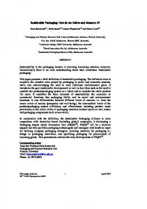
Performanceenhancing packaging Designing an IGBT module packaging for high-quality and reliable operation Daniel Schneider, Lydia Feller, Dominik Trüssel, Samuel Hartmann, Sven Klaka
The role of integrated circuits (IC) packaging has expanded from that of protecting the integrity and performance of an IC, to being a central factor in the development of electronic system concepts. In fact, packaging technology is now a prime design consideration if increasingly stringent performance and reliability requirements are to be met. Thanks to a combination of tighter process tolerances, more accurate material-property measurement, and more intelligent substrate design and simulation, companies are designing more cost-effective module packages that outperform the more expensive previous-generation units. The harsher the environment in which a module must function, the greater the demands on the packaging. The high reliability requirements specified by the traction and industrial markets means that the family of HiPakTM modules developed by ABB has to ensure safe operation, high isolation and high DC-current capability, as well as being long lasting.
ABB Review 3/2008
9
Performance-enhancing packaging
Semiconductors
A
BB’s family of HiPak modules are high-power insulated-gate bipolar transistors (IGBTs) in industry-standard housings, and are based on ABB’s own soft-punch-through (SPT) and SPT+ technologies 1 . With footprints of 190 by 140 mm and 130 by 140 mm, they cover a wide voltage range from 1,200 to 6,500 V, and a current range from 400 up to 2,400 A [1, 2]. In addition, three different isolation voltage categories of 4, 6.2 and 10.2 kVRMS are offered. These HiPak modules are built in single IGBT, dual IGBT, dual diode and chopper configurations. Because of its application in the traction and industrial markets, the packaging technology has to serve four main functions: It must provide a current path from the busbar to the chip and back. The module must have an effective cooling system to prevent overheating. The electrical contacts must be isolated from each other. The package needs to be mechanically robust. These functions are controlled in different parts of the HiPak module, a simplified cross section of which is shown in 2 . The parts in red illustrate the current path design, including the gate print, bond wires, and the main/ auxiliary terminals. The thermal path design, including the base-plate and ceramic substrate is shown in blue. The area in green illustrates the electric isolation design, which also con1
HiPak family
Firstly, a modular design means the main current path must be split into two. Wire bonds connect the chips with the substrate and main terminals connect the substrate with the busbar. Secondly, the mismatch in thermal expansion between silicon and the other packaging materials makes it necessary to design flexible current leads if stress on the solder joints is to be minimized. This flexibility means that long leads with a small cross sectional area are preferred. Because this results in high electrical resistance, a compromise must be found if low resistance is to be maintained.
stitutes the overall mechanical design, including the housing, silicone gel and epoxy filling.
The harsher the environment the greater the demands on the module packaging. As well as fulfilling the above-mentioned four functions, the package design should enable the module to operate for at least 30 years. An infinite lifetime is not possible because of thermal cycles. In other words, modules undergo power load cycles. A train, for instance, may stop at a station for two minutes, allowing the module to cool down by several tens of degrees. An overnight stop means the temperature of the module will decrease from over 100 °C to the ambient temperature. Such thermal cycles stress the module package in different ways. If two materials with different coefficients of thermal expansion (CTE) are joined together, they and the layer that joins them, for example solder joints, are particularly stressed whenever there is a temperature change. The contact between the bond wires and the chip metallization is also prone to failure when short cycles with low temperature differences are applied.
In today’s modules, a single terminal contact can have a rated current of up to 1,200 A. However, high ohmic heating in the terminal means the modules cannot be operated at these high currents over long periods of time without sufficient busbar cooling. An ideal high current design, which aims to maintain low electrical resistance between the busbar and the chip, is important because a large part of the ohmic heat generated in the terminals flows in the direction of the busbar.1) The maximum temperature difference in the terminal is limited on the one hand by the maximum allowable temperature of the packaging materials (for example the silicone gel) and on the other by the maximum allowable busbar temperature. In general, a maximum temperature difference of 50 K within the terminal
The current path design
The use of an ideal contact, consisting of a stiff and wide copper bar, is limited because of two issues: 2
Cross section of a HiPak IGBT module j
k
k
i
IGBT
h
g
diode
f
c
d e
b a
a
Cooler Base-plate c Solder d AIN-Ceramic insulator b
10
e
Cu metallization Silicone gel g Epoxy h Al bond wires f
i
Plastic casing Gate k Connection to bus bars j
ABB Review 3/2008
Performance-enhancing packaging
Semiconductors
The current path is defined by a geometry factor, ie, the ratio between its length and its cross sectional area. The terminals used today by ABB have a geomety factor of around 4,500 m-1 3 . The newer design has a geometry factor of 3,500 m-1. With no power flowing through the busbar, these values correspond to maximum DC currents of around 500 and 650 A, respectively. Stress relief for reliability
Optimization when designing the terminal leads is key to finding the right balance between low electrical resistance and good flexibility. The terminal, which is fixed in the plastic housing and soldered onto the substrate, is stressed by thermal cycles, which cause it to undergo a height change2). As solder joints are operated relatively close to their melting point, the stress they experience needs to be reduced to prevent their early failure. This is achieved by building so-called stress reliefs3) into the terminals. The force on the solder joint in several different designs has been evaluated using a standard tensile testing machine. Measurements after approximately 50 cycles, when the terminal is already strain-hardened, are shown in 4 . The blue curve shows an older terminal with a force of 100 N for a deflection of ± 0.5 mm. For the actual 3
terminal (in red), the same deflection corresponds to 50 N. This improved flexibility makes it possible to fulfill the reliability demands in passive thermal cycling and in active power cycling.
each other’s magnetic field. In the HiPak modules, this means having collector and emitter conductors in very close proximity. However, a minimum distance has to be maintained to prevent isolation damage.
Finding the balance between low electrical resistance and good flexibilty is key to terminal lead design.
Development trends
Bond wires
Bond wires also contribute to electrical resistance and as for the main terminals, the same trade-off situation applies. In bond wires, however, the stress is not induced through the package but instead through the large CTE mismatch between the aluminum bond wires and the silicon chip [3, 4]. The number and size of the bond wires are limited mainly by the space available on the active area of the chip. Nevertheless, a high current density within bond wires causes unwanted thermal stress. The crack in a bond wire, has propagated right through it 5 . Because of this, the bond wire is no longer usable.
The lower the thermal resistance between the IC and the cooling agent, the higher the output power of the module. Therefore, a good thermal contact will directly increase the module’s rating. A typical thermal impedance curve for IGBTs and diodes is shown in 6 . Within one second, thermal impedance reaches the static thermal resistance value. The time taken to reach stable temperatures is determined by the heat capacity of the Footnotes
Another very important issue affecting current path performance is the reduction in self inductance. The performance is considered good if conductors with current flowing in opposite direction are as close as possible to each other, thereby compensating
1)
4
60
1,200 A 800 400
Force (N)
200 150
Typically laminated busbars with a rated maximum temperature of between 105°C and 125°C are used.
2)
This height change is defined by the design of the package and depends on the temperature amplitude experienced by the package material.
3)
Stress reliefs are flexible parts with rather high electrical resistances.
Cycling measurement on main terminals with deflections of +/– 0.5 mm
300
Temperature difference (K)
The thermal path design
Self inductance
The maximum temperature difference in the terminal depending on its geometry; blue, green and red curves represent different DC currents.
250
Today’s ABB HiPak modules are rated for terminal currents of 800 A for IGBTs and 1,200 A for diodes. New chip technologies, however, require even higher terminal current ratings of 1,500 A for diodes and 1,200 A for IGBTs. The ongoing development towards higher operating temperatures increases the urgency to design terminals with lower resistance and better cooling.
0.6
New terminal Old terminal
40
0.4
20
0.2
0
0 -0.2
-20
100
cycle
cycle 49
cycle 50 -0.4
-40
50 0 0
1,000
2,000
3,000
4,000
5,000
Geometry factor = length / cross section (1/m)
ABB Review 3/2008
6,000
-60 1,680 1,700
Deflection (mm)
is permitted. If the resistance of the terminal connections is too high, the maximum DC current of the module is severely limited.
-0.6 1,720
1,740
1,760
1,780
1,800 1,820
Test time (s)
11
Performance-enhancing packaging
Semiconductors
materials. Therefore, the greater the amount of thermal mass close to the junction of the chip, the smaller the thermal ripples. Thermal resistance
In a water cooled system there are three comparable resistances in series, all of similar proportion: The first resistance lies inside the module between the junction of Crack in bond wire after active power cycling with ΔT of 55 K
5
Zth curve for a HiPak module
6
0.1
Zth j-c (KW) IGBT, Diode
Zth j-c Diode 0.01 Zth j-c IGBT
the chip and the casing (which happens to be the bottom of the baseplate.) The second is the contact resistance to the cooler The final resistance lies between the cooler surface and the ambient air. Of the three, the first is of most concern. To reduce thermal resistance, as is required in traction applications, the materials used have to be as thin and as thermally conductive as possible. To satisfy these requirements, all ABB modules use aluminum silicon carbide (AISiC)4) as the base-plate material and aluminum nitride (AIN) insulating substrates because of their excellent thermal cycling capability and low thermal resistance. Using materials in which there is a significant mismatch in CTE leads to delamination of the large soldering area below the substrate. Evidence of this is shown in the scanning acoustic microscopy (SAM) image of a module after 35,000 cycles with ΔT = 80 K 7 . Delamination can clearly be seen in the corners of the substrate. A solder thickness of 0.2 mm has been deemed necessary to achieve the highest possible cycling capabilities. Thinner solder layers place a lot of stress on the solder while thicker layers mean the larger CTE value of solder material starts to impact overall stress levels.
0.001
0.0001 0.001
0.01
0.1
1
1.1
l (s)
7
12
SAM image of an ABB HiPak module after 35,000 active power cycles with ΔT = 80 K. Note the lighter areas of delamination in the corners of the substrate.
To overcome some of these problems, certain improvements can be implemented. For example, substrates tend to tilt in the process and because of this, various distance holders are implemented [5]. Additionally, using solder with a higher melting point – because it has a better resistance against creep – would also help. Thermal mass
While making the materials thinner leads to a reduction in thermal resistance, it also has the effect of reducing the thermal mass close to the junction, which in turn can negatively impact factors such as reliability and surge current capability. In other words, small changes in power flow immediately translate into higher thermal cycles because the smoothing effect of the thermal mass on temperature peaks is missed.
Reliability
Active and passive cycling tests are conducted to test the HiPak module’s ability to withstand thermal cycles. In an active test, the modules are heated by passing a current through them. Each test is initially divided into short cycles lasting between one and five seconds where, due to the high thermal mass of the module, the chip is subjected to thermal cycles, the function of which is to stress the bondwire connections and the chip metallization. This is followed by longer cycles – in the range of one to two minutes – in which the chip and the rest of the package is exposed to the thermal cycle. This test serves to stress the solder joints.
The base-plate of all ABB modules is made from aluminum silicon carbide. To obtain the most accurate results, each failure mechanism should be individually investigated. A Weibull distribution detailing the failures of three different solder joints in the HiPak modules is shown in 8 . Delamination, which occurs in the large solder joint area between substrate and base-plate is highlighted in blue, the auxiliary pins that connect the substrates with the gate-print are highlighted in purple and finally, the main terminals that connect the substrates with the busbar are shown in green. A Weibull distribution allows engineers to predict when a certain percentage of the modules will fail, and it is common to use either one, five or 10 percent capability values. A user aiming for a failure rate of one percent within a 30-year lifetime would refer to the one percent value for his calculations. Development trends
Developing new materials is one way of improving reliability and overcoming the problems associated with thermal resistance and thermal mass. New metal matrix composite (MMC) materiFootnote 4)
AISiC material has an ideal combination of high thermal conductivity, low CTE and stiffness.
ABB Review 3/2008
Performance-enhancing packaging
Semiconductors
als, where diamond replaces silicon carbide, are currently in development. Optimized soldering processes are constantly being sought to prevent tilting. Soldering could even be replaced by using welding techniques for terminals or by low temperature bonding for larger areas. Encapsulation
The purpose of encapsulating IGBT modules is three-fold: it isolates different potentials, protects the devices from moisture and contaminants, and reduces mechanical stresses.
Simulation testing reveals no degradation in module insulation.
Isolation
In high voltage modules, potential differences of 6.5 kV appear over a distance of only 2 mm. To ensure adequate isolation under severe mechanical and chemical stress over the 30-year operational lifetime of the module, the materials involved in the module design need to be carefully selected. Inside the module, isolation is normally achieved using ceramic and plastic materials. If secure insulation is to be ensured, these materials need to be processed with void-free interfaces and must adhere perfectly to each other and to metal surfaces. Polyimide is used in areas where the electrical field is greatest. However, it is used only in layers that are approximately 10µm thick. The rest of the module space is filled with silicone gel. The module exterior has to fulfill the clearance and creepage distances defined by the insulation coordination 8
standards (EN 50124-1). For high-voltage applications, the choice of housing material is severely limited because a comparative tracking index (CTI) of 600 V is required to fulfill this standard. However, even with materials in the highest CTI class, equal to or above 600 V, very long creepage distances are required. This leads to the design of grooves, which is typical for high-voltage modules 1 .
The modules need to maintain their insulating capabilities throughout their lifetime and so different tests were carried out to ensure insulation quality. For example, the quality of the insulation between the collector and emitter current leads was tested successfully with high temperature reverse bias (HTRB) qualification runs at 125 °C for 1,000 hours. Additional testing was also carried out on the insulation between the baseplate, which is at the same potential as the cooler, and the current leads. The insulation test was done at 10.2 kVrms for the high insulation versions including some 3.3 kV and all 6.5 kV modules. The large electrical fields that occur during this test are indicated in 9 . Close to the triple point ceramic-copper-polyimide, the field exceeds 20 kV/mm. All modules have been subjected to a partial discharge test, which prevents any long-term damage caused by repetitive discharges that eventually erode the
Different failure mechanisms for failures in active power cycling with ΔT = 80 K
9
insulating materials. Severe power cycling tests are used to simulate the lifetime of a module. ABB has measured module insulation characteristics after these tests and found no evidence of degradation. The mechanical design
To make use of the full cycling capability offered, the HiPak module has to operate safely in harsh, humid and chemical environments or when it is mechanically stressed from the outside until it reaches the end of its innate life.
Encapsulating IGBT modules protects the device from moisture and contaminants, reduces mechanical stresses and isolates different potentials. The impact of humidity on module functionality has been tested in a temperature humidity bias test (THB). More severe testing has been undertaken in harsher environments such as salt mist or sulfur, in all of which the module survived. The modules have also been tested for the effects of mechanical stress. Because the terminal connections of the module make contact with the gate units and the busbars, they are able to transmit mechanical stresses to the module in a rather undefined manner. To test the modules resistance against these stresses, shock and vibration testing
Simulation of two-dimensional electric field for a substrate
99
Percent
63
20 10 Delamination Aux pin solder Main terminal solder
5 2 1 10,000
15,000
20,000
30,000
40,000
60,000
Cycles to failure (ΔT = 80K)
ABB Review 3/2008
13
Performance-enhancing packaging
Semiconductors
was performed. To make the test more stressful, the HiPak modules were loaded with additional two kilogram bars on the main terminals and 250 g bars on the auxiliary terminals. Despite these severe conditions, absolutely no problems were detected. This outstanding performance is possible, thanks to a thick epoxy layer filled with glass fibers and minerals.
10
traction. Robustness translates into higher operating safety margins and allows low gate drive resistance at turn-off, which, in turn, allows lower turn-off losses. This is in keeping with ABB’s reputation for offering high power semiconductors of exceptionally high reliability for the harshest of conditions.
Overview of ABB’s qualification program for HiPak modules
Test Conditions
Standard Active power cycling (case)
tcycle = 1-2 mins, ΔTcase = 60-80 K
IEC 60747-9, 60749-34
Active power cycling (junction) tcycle = 1-5 s, ΔTj = 40-80 K
IEC 60747-9, 60749-34
Passive thermal cycling tcycle = 4 h, ΔT = 165-200 K
An overview of the characteristics of the HiPak product family is given in 10 .
IEC 60068-2-14
High temperature reverse bias
Unfortunately, a good design IEC 60747–9.8 Vce = 5200 V, 125°C, 1000 h and thorough testing cannot High temperature gate bias guarantee zero failures. In Vge = +/-20 V, 125°C, fact, standard failure rates IEC 60749-9.8 1000 h are of the order of several Temperature humidity bias hundred failures in time Vce = 80 V, 85°C, 85%, (FITs), where one FIT equals IEC 60749–3.4B 1000 h one module failure in one Salt mist billion device-operating hours. In this case, it is im50 g/l NaCl, 35°C, 16 h IEC 60068-2-11 portant that the modules fail Sulfur (SO2, H2S) safely, with the lowest possi25°C, 75 percent, 10 days IEC 60068-2-60 ble impact on neighboring Shock and vibration equipment and with zero impact on human beings. IEC 61373 Therefore, ABB has chosen Fire protection a robust design with a thick UL 94 : V0, epoxy layer, which helps to NF F 16-101 : I3/F2 absorb (while directing sideways) energy in case of an explosion. Furthermore, the and higher currents leads to the ohmic chosen materials have been certified heating of terminals. In other words, according to the flammability stanencapsulation materials are expected dards (UL 94 and NF F 16-102). Thereto perform very well at both low and fore in the case of a fire, the materials high temperatures. extinguish without developing toxic gases.
ABB’s HiPak family of IGBT modules sets new standards of robustness for reliability in harsh conditions.
For more on IGBTs, see “Switching to higher power” on page 19 of this issue of ABB Review.
Daniel Schneider Lydia Feller Dominik Trüssel Samuel Hartmann Sven Klaka
Setting new standards
ABB Semiconductors
To find the right compromise between performance and reliability, different design variants have to be considered. ABB’s HiPak family of IGBT modules sets new standards of robustness for high reliability applications such as
Lenzburg, Switzerland
[email protected] [email protected] [email protected] [email protected] [email protected]
References
Development trends
Two development directions are important for encapsulation. To enable operation in Siberia and Tibet, the storage or operating temperature range has been extended down to – 55 °C. At the other extreme, the trend towards higher operating temperatures of up to 150 °C and beyond, 14
[1] Rahimo, M. et al. (2004). 2.5 kV–6.5 kV Industry standard IGBT modules setting a new benchmark in SOA capability. Proc. PCIM, 314–319, Nürnberg, Germany. [2] Rahimo, M. et al. (2005). SPT+, The next generation of low-loss HV-IGBTs. Proc. PCIM, 361–366, Nürnberg, Germany. [3] Yamada, Y. et al. (2007). Reliability of wire-bonding and solder joint for high temperature operation of power semiconductor device, Microelectronics Reliability 47 2147–2151. [4] Horio, M. et al. (2007). Investigations of high temperature IGBT module package structure. Proc. PCIM, Nürnberg, Germany. [5] K. Guth, K., Mahnke, P. (2006). Improving the thermal reliability of large area solder joints in IGBT power modules. Proc. CIPS, Naples, Italy.
ABB Review 3/2008