Generator. Product Description. P1P3800A is a Phase Synchronizing clock
generator that generates four outputs from an input clock. Output frequency will
be a ...
P1P3800A Phase Synchronizing Clock Generator Product Description
A = Assembly Location L = Wafer Lot Y = Year W = Work Week G = Pb−Free Package (Note: Microdot may be in either location)
CLKOUT2
PIN CONFIGURATION
12
11
10
S2 1 S1 2
9 PD# P1P3800A
CLKIN 3 4
Application
• P1P3800A can be used in applications where Phase Synchronization is needed.
8 CLKOUT4 7 CLKOUT3
S3
• • • • • • • •
60 Hz − 120 Hz 4 Clock Outputs 4 Two Level Controls to Select Sets of Clock Outputs Output Buffer Drive Strength: 8 mA Supply Voltage: 3.8 V − 5.5 V Power Down for Power Save 12−Lead 3mmx3mm WQFN Package Operating Temperature Range: -40°C to +85°C These Devices are Pb−Free, Halogen Free/BFR Free and are RoHS Compliant
WQFN12 CASE 510AH
5
6 S4
120 Hz − 240 Hz (External Reference Clock)
• Output Clock Frequency:
P1P 3800A ALYWG G
1
V DD
• Input Clock Frequency:
MARKING DIAGRAM
GND
Features
http://onsemi.com
CLKOUT1
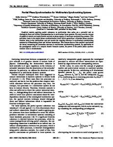
P1P3800A is a Phase Synchronizing clock generator that generates four outputs from an input clock. Output frequency will be a divide by two of the input clock. The phase of the output clocks is selectable through four select signals S1, S2, S3 and S4. Refer to Output Clock Selection Table. The outputs will go ‘low’ when all the select signals are ‘low’. The transition to a new state of the output will be ‘glitch free’ when the select inputs change state. A Power Down signal enables the device to be driven to a power save mode, when active. The device works over a supply voltage range of 3.8 V − 5.5 V. The device is available in a 12−Lead 3mmx3mm WQFN package and operates over -40°C to +85°C.
(Top−View)
S [1:4]
PD#
Digital Logic & Divider
CLKIN
ORDERING INFORMATION
VDD
See detailed ordering and shipping information in the package dimensions section on page 6 of this data sheet.
CLKOUT [1:4]
GND
Figure 1. Block Diagram
© Semiconductor Components Industries, LLC, 2012
January, 2012 − Rev. 1
1
Publication Order Number: P1P3800A/D
P1P3800A Table 1. PIN DESCRIPTION Pin#
Pin Name
Type
1
S2
I
Output clock select. Refer Output Clock selection table. Has NO default state
Description
2
S1
I
Output clock select. Refer Output Clock selection table. Has NO default state.
3
CLKIN
I
External Reference Clock Input
4
S3
I
Output clock select. Refer Output Clock selection table. Has NO default state.
5
GND
P
Ground to entire chip
6
S4
I
Output clock select. Refer Output Clock selection table. Has NO default state.
7
CLKOUT3
O
Buffered clock output. Refer CLKOUT Diagram
8
CLKOUT4
O
Buffered clock output. Refer CLKOUT Diagram
9
PD#
I
Power Down. Powers down the entire chip when pulled LOW. CLKOUT [1:4] will be LOW when power down is enabled. Has NO default state.
10
CLKOUT2
O
Buffered clock output. Refer CLKOUT Diagram
11
VDD
P
Supply Voltage
12
CLKOUT1
O
Buffered clock output. Refer CLKOUT Diagram
Table 2. OUTPUT CLOCK SELECTION TABLE S4
S3
S2
S1
CLKOUT4
CLKOUT3
CLKOUT2
CLKOUT1
0
0
0
0
Low
Low
Low
Low
0
0
0
1
CLK#
CLK#
CLK#
CLK
0
0
1
0
CLK#
CLK#
CLK
CLK#
0
0
1
1
CLK#
CLK#
CLK
CLK
0
1
0
0
CLK#
CLK
CLK#
CLK#
0
1
0
1
CLK#
CLK
CLK#
CLK
0
1
1
0
CLK#
CLK
CLK
CLK#
0
1
1
1
CLK#
CLK
CLK
CLK
1
0
0
0
CLK
CLK#
CLK#
CLK#
1
0
0
1
CLK
CLK#
CLK#
CLK
1
0
1
0
CLK
CLK#
CLK
CLK#
1
0
1
1
CLK
CLK#
CLK
CLK
1
1
0
0
CLK
CLK
CLK#
CLK#
1
1
0
1
CLK
CLK
CLK#
CLK
1
1
1
0
CLK
CLK
CLK
CLK#
1
1
1
1
CLK
CLK
CLK
CLK
http://onsemi.com 2
P1P3800A CLKOUT Diagram CLK
CLK#
LOW
TIMING Diagram For Glitch Free Operation (For Reference) (Transition of outputs from any state to any other state)
S4=1, S3=1, S2=1, S1=0
Change Area
S4=1, S3=1, S2=0, S1=1
Change Area
S4=0, S3=0, S2=1, S1=1
PD#
Latency
Latency
PD#=0
Input Clock CLKOUT1
CLKOUT2
CLKOUT3
CLKOUT4
Note: Transition to new state will happen after a latency of one output clock cycle after completing the present output clock cycle Transition to new state will happen after a latency of up to 3 input clock cycles excluding the input cycle where the transition has occured.
Power Up 10mS(min) VDD I/P CLK
CLKOUT S1~S4 in any stable state
Valid Clock according to S1~S4
Note: Transition to new state will happen after a latency of up to 2 input clock cycles excluding the input cycle where the transition has occured.
http://onsemi.com 3
P1P3800A PD# Operation 10mS(min)
PD#
I/P CLK
CLKOUT Valid Clock according to S1~S4
S1~S4 in any stable state
Note: Transition to new state will happen after a latency of up to 2 input clock cycles excluding the input cycle where the transition has occured.
http://onsemi.com 4
P1P3800A Table 3. OPERATING CONDITIONS Symbol
Min
Max
Unit
Supply Voltage
3.8
5.5
V
TA
Operating Temperature
−40
+85
°C
CL
Load Capacitance
15
pF
CIN
Input Capacitance
7.0
pF
VDD
Parameter
Table 4. ABSOLUTE MAXIMUM RATINGS Symbol
Rating
Unit
VDD
Voltage on VDD pin with respect to Ground
−0.5 to +7.0
V
VIN
Voltage on any input pin with respect to Ground
−0.5 to +4.0
V
Storage Temperature
−65 to +125
°C
TSTG
Parameter
Ts
Max. Soldering Temperature (10 sec)
260
°C
TJ
Junction Temperature
150
°C
Static Discharge Voltage (As per JEDEC STD22−A114−B)
2.0
kV
TDV
Stresses exceeding Maximum Ratings may damage the device. Maximum Ratings are stress ratings only. Functional operation above the Recommended Operating Conditions is not implied. Extended exposure to stresses above the Recommended Operating Conditions may affect device reliability.
Table 5. DC ELECTRICAL CHARACTERISTICS Symbol
Parameter
Min
Typ
Max
Unit
3.8
5.0
5.5
V
GND − 0.3
0.8
V
1.6
3.0
V
Input Low Current
10
mA
IIH
Input High Current
10
mA
0.4
V
VDD
Operating Voltage
VIL
Input Low Voltage (Note 1)
VIH
Input High Voltage (Note 1)
IIL VOL
Output Low Voltage
IOL = 8 mA
VOH
Output High Voltage
IOH = −8 mA
ICC
Power Down Current (PD# pulled to GND)
IDD
**Dynamic Supply Current, PD# = 5.5 V; S[1:4] = 5.5 V/GND; CLKIN Swing = 0 to 5.5 V; VDD = 5.5 V
1.8
Dynamic Supply Current, PD# = 3 V; S[1:4] = 3 V/GND; CLKIN Swing = 0 to 3.0 V
3.0
Dynamic Supply Current, PD# = 3 V; S[1:4] = 1.6 V; CLKIN Swing = 0 to 1.6 V
4.0
Dynamic Supply Current, PD# = S[1:4] = 1.6 V; CLKIN Swing = 0 to 1.6 V
5.0
VDD − 0.6*
V 1.0
*For VDD = 5 V, VOH = VDD − 0.4 V. **Indicative value, not a recommended operating condition. 1. Parameter is guaranteed by design and characterization. Not tested in production.
http://onsemi.com 5
mA mA
P1P3800A Table 6. AC ELECTRICAL CHARACTERISTICS Symbol CLKIN CLKOUT
Max
Unit
Input Clock Frequency
Parameter
Min 120
Typ
240
Hz
Output Clock Frequency
60
120
Hz
tLH, tHL
Output Rise / Fall time (Measured from 20% to 80%) (Notes 1, 2)
10
ms
tLH, tHL
Input Rise / Fall time (Measured from 20% to 80%)
50
ms %
tDOUT
Output Duty Cycle (Measured at VDD/2) (Notes 1, 2)
49
50
51
tDIN
Input Duty Cycle
49
50
51
tsu
Set up time for control signals, S[1:4], PD# to input clock rising edge (Note 1)
60
ms
th
Hold up time for control signals, S[1:4], PD# to input clock rising edge (Note 1)
60
ms
tskew
Output−Output Clock Skew (Note 1)
10
%
ms
2. All parameters are specified with 15 pF loaded output.
Typical IDD Vs PD# Input Voltage Plot
ORDERING INFORMATION Part Number P1P3800AG12CRTWG
Package
Shipping†
12 pin (3 mm x 3 mm) WQFN
3000 / Tape & Reel
†For information on tape and reel specifications, including part orientation and tape sizes, please refer to our Tape and Reel Packaging Specifications Brochure, BRD8011/D.
http://onsemi.com 6
P1P3800A PACKAGE DIMENSIONS WQFN12 3x3, 0.5P CASE 510AH ISSUE O
ÇÇÇ ÇÇÇ ÇÇÇ
D
PIN ONE REFERENCE
2X
L
B
A
L1 DETAIL A ALTERNATE CONSTRUCTIONS
E
ÇÇÇ ÉÉÉ ÉÉÉ
0.10 C
2X
EXPOSED Cu
0.10 C
TOP VIEW A
DETAIL B
0.10 C
13X
0.10 C
A1
NOTE 4
C
SIDE VIEW
MOLD CMPD
DETAIL B
A3
ÉÉ ÇÇ ÇÇ
A3
A1
ALTERNATE CONSTRUCTIONS
DIM A A1 A3 b D D2 E E2 e K L L1
MILLIMETERS MIN MAX 0.65 0.85 0.00 0.05 0.22 REF 0.20 0.30 3.00 BSC 1.30 1.50 3.00 BSC 1.30 1.50 0.50 BSC 0.20 −−− 0.30 0.50 0.00 0.15
SOLDERING FOOTPRINT*
SEATING PLANE
12X
0.63
PACKAGE OUTLINE
D2
DETAIL A
NOTES: 1. DIMENSIONING AND TOLERANCING PER ASME Y14.5M, 1994. 2. CONTROLLING DIMENSION: MILLIMETERS. 3. DIMENSION b APPLIES TO PLATED TERMINAL AND IS MEASURED BETWEEN 0.15 AND 0.30 MM FROM TERMINAL TIP. 4. COPLANARITY APPLIES TO THE EXPOSED PAD AS WELL AS THE TERMINALS.
L
12X
4
L 1 2X
7 12X
E2 1
b 0.10 C A B 0.05 C
K
2X
1.50 3.30 12X
0.30
NOTE 3
12
0.50 PITCH
e
DIMENSIONS: MILLIMETERS
BOTTOM VIEW
*For additional information on our Pb−Free strategy and soldering details, please download the ON Semiconductor Soldering and Mounting Techniques Reference Manual, SOLDERRM/D.
ON Semiconductor and are registered trademarks of Semiconductor Components Industries, LLC (SCILLC). SCILLC reserves the right to make changes without further notice to any products herein. SCILLC makes no warranty, representation or guarantee regarding the suitability of its products for any particular purpose, nor does SCILLC assume any liability arising out of the application or use of any product or circuit, and specifically disclaims any and all liability, including without limitation special, consequential or incidental damages. “Typical” parameters which may be provided in SCILLC data sheets and/or specifications can and do vary in different applications and actual performance may vary over time. All operating parameters, including “Typicals” must be validated for each customer application by customer’s technical experts. SCILLC does not convey any license under its patent rights nor the rights of others. SCILLC products are not designed, intended, or authorized for use as components in systems intended for surgical implant into the body, or other applications intended to support or sustain life, or for any other application in which the failure of the SCILLC product could create a situation where personal injury or death may occur. Should Buyer purchase or use SCILLC products for any such unintended or unauthorized application, Buyer shall indemnify and hold SCILLC and its officers, employees, subsidiaries, affiliates, and distributors harmless against all claims, costs, damages, and expenses, and reasonable attorney fees arising out of, directly or indirectly, any claim of personal injury or death associated with such unintended or unauthorized use, even if such claim alleges that SCILLC was negligent regarding the design or manufacture of the part. SCILLC is an Equal Opportunity/Affirmative Action Employer. This literature is subject to all applicable copyright laws and is not for resale in any manner.
PUBLICATION ORDERING INFORMATION LITERATURE FULFILLMENT: Literature Distribution Center for ON Semiconductor P.O. Box 5163, Denver, Colorado 80217 USA Phone: 303−675−2175 or 800−344−3860 Toll Free USA/Canada Fax: 303−675−2176 or 800−344−3867 Toll Free USA/Canada Email:
[email protected]
N. American Technical Support: 800−282−9855 Toll Free USA/Canada Europe, Middle East and Africa Technical Support: Phone: 421 33 790 2910 Japan Customer Focus Center Phone: 81−3−5817−1050
http://onsemi.com 7
ON Semiconductor Website: www.onsemi.com Order Literature: http://www.onsemi.com/orderlit For additional information, please contact your local Sales Representative
P1P3800A/D