This paper proposes a practical methodology to evaluate the shortâcircuit power of static CMOS gates via effective use of timing information from timing analysis.
Predicting Short Circuit Power From Timing Models Emrah Acar, Ravishankar Arunachalam* and Sani R. Nassif IBM Research, Austin *IBM Corporation (emrah, ravaru, nassif)@us.ibm.com 11501 Burnet Rd. Austin, TX 78758
Abstract− Power dissipation is becoming a major show stopper for integrated circuit design especially in the server and pervasive computing technologies. Careful consideration of power requirements is expected to bring major changes in the way we design and analyze integrated circuit performance. This paper proposes a practical methodology to evaluate the short−circuit power of static CMOS gates via effective use of timing information from timing analysis. We introduce three methods to estimate short−circuit power of a static CMOS circuit without requiring explicit circuit simulation. Our proposed methodology offers practical advantages over previous approaches, which heavily rely on simple special device models. Proposed approach is experimented with an extensive set of benchmark examples and several device models and found very accurate.
I. Introduction During input signal transitions, both the NMOS and PMOS blocks in static CMOS circuits conduct simultaneously for a short period of time causing a direct current flow from power rails, resulting in short−circuit power. Prediction of short−circuit power is of increasing importance as power shows signs of limiting circuit performance. Many experts expect that scaling trends would make short−circuit power as important as the dynamic power dissipated in a logic stage [1]. In this paper, we propose a methodology to predict the short− circuit power based on industry recognized timing models. Typically, a substantial effort is spent for timing verification for modeling in the industry. Hence, many integrated device manufacturers and fabless design companies make extensive use of timing libraries in their verification flows. A typical timing library models the gate delay under various input and load conditions. Common engineering practice, yet at first order, characterizes the gates per each input signal switching, and the output waveform is often approximated by a piecewise linear waveform with several selected datapoints. Typically the timing models include average gate delay, measured at 50% of the full logic value, and the output slew for pre−characterized datapoints. The typical timing rules can be formulated similar to the equations below: t out,50 =F 1 t in, slew ,C L t out,slew =F 2 t in,slew , C L (1) where C L is the load capacitance and t in,slew is the input slew (transition time). Traditionally, F 1 and F 2 are selected as polynomial functions or stored in multi−dimensional tables. The function arguments may also include other parameters such as Vdd. Characterized functions for (1) are heavily used in static
timing analysis, which is part of the state−of−art sign−off methodology. In a similar manner, short−circuit power for each gate can be pre−characterized for each switching input signal as Dartu discusses in [2]. For average short−circuit power, simple polynomial models have been proposed, but unlike timing models, pre−characterized short−circuit power models are not well adapted, and are not part of the standard gate libraries. In fact, most of the previous research on short−circuit power have focused on closed−form analytical expressions , even for an equivalent inverter circuit model using simplified device models, primarily to obtain a basic device−centric intuition for the short− circuit power. Most notably, [3] uses Shichman−Hodges model, and [4,5] use the alpha−power law model described in [6] for previous models. These approaches generally attempt to solve the set of differential equations for a switching inverter loaded with a nominal load capacitance. However, the accuracy and efficiency of their formulas largely depend on speculated simple device models and assumptions made for the device operation during signal transitions. For example, [4,5,7,8,9] all evaluate inverter output waveform under the assumption of zero PMOS device current in order to obtain a solvable closed−form differential equation for output waveform. Then, the output waveform expression is used to deduce actual nonzero PMOS current for time−domain integration which results in total short−circuit power for the signal transition. Most recently in [10], a more complex model (MM9 [11]) is incorporated with alpha−power model. Our goal in this paper is not to obtain a closed−form expression, but instead to layout a practical methodology for evaluating the short−circuit power of typical static CMOS circuits whose timing models are available. With the described methodology, we propose a practical and useful way to get around incomplete performance characterizations. We focus on the inverter circuit model with general RC loads, since for the power−perspective, the static CMOS gates can be macromodeled as an inverter for each input combination [12]. One significant advantage of our approach is the utilization of general device models, or general device i−v characteristics instead of building the model upon a simplified lower dimensional device model. This offers more promising applicability for circuit designers who can only use established timing models and typical device model cards in their analyses. Section II summarizes the short−circuit current for static CMOS inverters. In section III, we briefly discuss previous work in the field. In section IV, the proposed methodology is outlined in detail. The results and findings are presented and discussed in section V. In section VI, we conclude with final remarks and outline some future directions.
Isc(t) Vin
Load
2
Vout(t)
input output 1000 I_sc 1000 I_sc of pwl i/o SC interval pwl output
Vin(t) Isc(t)
Vout(t)
0.8
TR TF+DF t1
0 DF t0
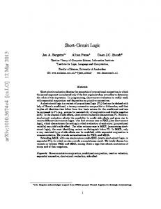
Fig. 1. Inverter model with input and output waveforms.
time(s) −0.2 0e+00
In a static CMOS logic gate, the short−circuit current, I SC is observed when both NMOS and PMOS devices form a DC path between power rails. The power associated with this current is referred to as short−circuit power. Since this power is delivered by the voltage supply ( V DD ), the total short−circuit power (total energy per transition) can be written as P SC =V DD ∫T I SC τ d τ (2) where T is the switching period. In power analysis, the short− circuit power P SC must be added to P D , the power required to charge/discharge the load capacitance. P D and P SC are both considered dynamic, whereas leakage is considered as a static phenomenon. In Fig. 1, a simple inverter is driven by a rising ramp input, resulting in a short−circuit current, I SC on the PMOS device. Assuming the input signal begins to rise at origin, the time interval for short−circuit current starts at t 0 when the NMOS device turns on, and ends at t1 when the PMOS device shuts off. During this time interval, the PMOS device moves from linear region operation to saturation (unless an exceptionally fast input causes the device to shut off before the output voltage starts falling). Based on the ramp input signal with a rise time T R , t 0 and t 1 can be expressed as: V thn
t 1 =T R
V DD
V DD �V thp V DD
(3)
The average short−circuit power can be specified as the integral of short−circuit current between t 0 and t 1 : P SC =V DD ∫t I SC τ d τ ⁄ t 1�t 0 t1
4e−10
Fig. 2. Input and output waveforms and the short circuit current for two different input−output signal pairs.
II. Short Circuit Current
t 0=T R
2e−10
(4)
0
III. Previous Approaches One of the earliest approaches to modeling short−circuit power is presented in [3]. Using the inverter model with a basic device model, a fairly simple formula for P SC is given. This formula assumes that the PMOS device operates in saturation during the short−circuit current interval. This simple model does not account for load capacitance and is very inaccurate for short channel devices. Vemuri proposed a more accurate model [4], which uses the alpha−power law model. In this model the output waveform is solved explicitly by neglecting the short−circuit current. The output waveform is then used to evaluate I SC with the alpha−power law model and several approximations for the integration for P SC are presented. In [8], a similar model is derived for the pi CRC load model. This work makes a triangular
approximation of I SC to calculate the power. Most recently, [5] proposed updated formulas for the short−circuit power model of an inverter with alpha−power law device models. In previous approaches, simplified device models are extensively used to develop closed−form formulas, or generate analytical relationship between device models and the short− circuit power. They are also used to compare the models with actual circuit simulation results. While these works are important for early estimation and trend analysis for CMOS technologies, they fail to be effective during the actual design verification process. The primary reason is that present−day device models tend to be much more complex than the ones assumed. Another difficulty observed is the need for a conversion, or extraction tool that produces an equivalent alpha−power model from the actual device models, which may well be opaque to the user (like BSIM). Another mentionable concern with existing power models is the treatment for complex interconnect RC(L) loads which critically influence deep submicron delays.
IV. Proposed Methodology A. Signal Abstractions In digital design, electrical signals are often approximated by piecewise linear waveforms for visualization and timing related computations. This simplification brings several advantages in representing the circuit performance by a few simple temporal variables, such as delay and slew. Unlike its popular use, the piecewise linear waveform modeling can bring about severe inaccuracies for short−circuit power evaluation. Fig. 2 shows the input−output behavior of an inverter driving a pi−load. The data is taken for 0.5 micron technology node and the input signal is assumed as a saturated ramp. Fig. 2 also shows an enlarged trace of short−circuit current ( 1000 I sc ) from supply to ground through the PMOS device. All waveforms in Fig. 2 are obtained by circuit simulation (SPICE) using level 3 device models. This figure also shows the piecewise linear abstraction for the output waveform as a falling transition, matching the 50% point of the output. The output slope is calculated using 20% and 80% of the full logic value. When we use the piecewise linear output waveform to calculate the short− circuit current, the v ds of the PMOS device would be approximated as zero for a brief time interval, causing zero short−circuit current. By enforcing the piecewise linear input and output waveforms, another short−circuit power waveform is generated via circuit simulation. As shown in the Fig. 2 1000 I sc of pwl i ⁄ o the piecewise linear output waveform approximation clearly underestimates the area beneath the I ds curve, and therefore the total short−circuit power and energy.
Note that the inaccurate piecewise linear model manages to predict the maximum short circuit current very closely. Note also that the base of the short−circuit current waveform is closely related to the threshold voltages of the devices and mostly depends on the input signal. These observations motivate us to search for the maximum value of short−circuit current using the abstractions of input and output signal waveforms. For simplification, we will describe the methodology for static CMOS inverters of which the input and output signal waveforms are characterized as piecewise linear functions. The generalization for other gates is possible by transforming the CMOS gate into an equivalent inverter preserving the delay and supply current [12]. Since most of pre− characterization for the static timing analysis is performed for each timing arc on a single input−output pair, the equivalent inverter macro−modeling appears to be practically feasible. We believe that an inverter model for a general gate will yield sufficiently valid results for power performance. Similarly, other generalizations of waveform models are also applicable within the framework discussed below.
simulation tools. The evaluation of the device current for a particular configuration can be interpolated from the sampled data points stored in a table. Such tables may be constructed for different device sizes, or proper scaling formulas can be used. For the inverter circuit shown in Fig. 1, the timing models approximate the output waveform by a saturated ramp function: V dd v out t = V dd 1� t �D F ⁄T F pwl
Equation (5) can be written as complex as possible to cover all three distinct operation modes (cut−off, linear region and saturation) with great accuracy. The vector p dev includes the device−related and environmental parameters that affect the device operation. Examples for such parameters are temperature, oxide thickness, channel length reduction factor. Hence, p dev vector can be considered as the device model parameters entered in a typical SPICE card. The other mathematical equation concerns about the operating regime of the MOSFET device. Generally, the device is assumed to be active in both linear region and saturation regions. The operating regime also depends on the device model characteristics and terminal voltages. However, the relation between the operating regime and device model parameters is often simpler than (5). For example, according to Shichman− Hodges device model, the NMOS device is operating in the saturation region if the following functional is positive: g v ds, v gs, v sb, p dev =v ds � v gs �v th >0 (6) where v th is the threshold voltage, and can be directly calculated from the arguments. For another example, alpha−power law model models the device in the saturation region when it sees a positive value of α α⁄ 2 g v ds, v gs, v sb, p dev =v ds � pv v gs �v th >0 (7) where pv and α are elements of p dev . Throughout this paper, we make use of the fact that g function is relatively simpler. We assume that the timing models for all different gates are available in the form (1), and the equivalent inverter representations are known. Furthermore, we will assume that efficient implementations of the device model f and g are given. One of the most practical ways to implement f is the use of multi−dimensional tables as done in many timing
(8)
D F �T F ≤t
0
(8) approximates drain−source terminal voltage of the PMOS pwl pwl device as v ds t =V dd �v out t . The time offset ( D F ) and the output slew ( T F ) are direct outputs of the timing model. In the case of a ramp input with a rise time T R , the input waveform is also a linear function of time: 0 v
pwl in
B. Assumptions on Device Modeling In our methodology, the NMOS and PMOS device models are assumed to be quite general to cover existing device technologies. In general, behavior of a MOSFET device is represented by a set of nonlinear relations corresponding to multiple operating regimes. Since the drain−current source is the primary output of most of the existing models, we will use the following model for MOSFET device: (5) I ds = f v ds, v gs, v sb, p dev
t