REVIEWS Printing, folding and assembly methods for forming 3D mesostructures in advanced materials Yihui Zhang1, Fan Zhang1, Zheng Yan2, Qiang Ma1, Xiuling Li3, Yonggang Huang4 and John A. Rogers5
Abstract | A rapidly expanding area of research in materials science involves the development of routes to complex 3D structures with feature sizes in the mesoscopic range (that is, between tens of nanometres and hundreds of micrometres). A goal is to establish methods for controlling the properties of materials systems and the function of devices constructed with them, not only through chemistry and morphology, but also through 3D architectures. The resulting systems, sometimes referred to as metamaterials, offer engineered behaviours with optical, thermal, acoustic, mechanical and electronic properties that do not occur in the natural world. Impressive advances in 3D printing techniques represent some of the most broadly recognized developments in this field, but recent successes with strategies based on concepts in origami, kirigami and deterministic assembly provide additional, unique options in 3D design and high-performance materials. In this Review, we highlight the latest progress and trends in methods for fabricating 3D mesostructures, beginning with the development of advanced material inks for nozzle-based approaches to 3D printing and new schemes for 3D optical patterning. In subsequent sections, we summarize more recent methods based on folding, rolling and mechanical assembly, including their application with materials such as designer hydrogels, monocrystalline inorganic semiconductors and graphene.
Center for Mechanics and Materials, AML, Department of Engineering Mechanics, Tsinghua University, Beijing 100084, China. 5 Departments of Materials Science and Engineering, Biomedical Engineering, Neurological Surgery, Chemistry, Mechanical Engineering, Electrical Engineering and Computer Science; Center for BioIntegrated Electronics; and Simpson Querrey Institute for BioNanotechnology, Northwestern University, Evanston, Illinois 60208, USA. 1
Correspondence to Y.Z. and J.A.R.
[email protected];
[email protected] doi:10.1038/natrevmats.2017.19 Published online 29 Mar 2017
The development of strategies for forming 3D microand nanostructures in advanced materials is of increasing interest, driven by the potential for creating material systems with fundamentally new characteristics and functionalities. The notion of engineered materials, sometimes referred to as metamaterials1–5, has its most prominent origins in electromagnetic structures with properties that do not occur naturally, such as negative refractive index 4 and artificial magnetism2. Here, extended 3D arrays of interconnected features with dimensions in the subwavelength regime allow exquisite control over the propagation of electromagnetic waves, with impressive examples in the microwave4,6–8, terahertz9–11, and infrared and visible12–16 regions of the electromagnetic spectrum. The required length scales span a wide range, from a few millimetres to tens of nanometres. The challenges in growth, assembly and/or fabrication are daunting, in which solutions require fundamental, conceptual advances in mat erials science and engineering. As examples, routes to 3D micro- and nanostructures for photonics include
NATURE REVIEWS | MATERIALS
colloidal self-assembly 17, holographic lithography 18–21, direct-semiconductor or layer‑by‑layer growth22–25, and two- or multiphoton lithography 26–29. Fabrication typically begins with formation of the necessary 3D architectures in materials optimized for this purpose, followed by exchange and/or templated growth to convert these materials into those required to yield desired optical responses. For example, two- or multiphoton lithography provides a means for patterning 3D structures with geometries suitable for photonic bandgap behaviour, but only in specialized, photosensitive materials that do not possess a sufficiently high dielectric constant. Therefore, these 3D structures are often used as templates for forming thin films of metals or semiconductors by atomic layer or chemical vapour deposition30–32. Modern use of the term ‘metamaterial’ spans mat erials that have structurally engineered behaviours in any property of interest, including optical12–16, thermal33–35, acoustic36–39, mechanical40–48 and electromagnetic4,6–8. Progress in nearly all cases relies critically on developments in materials and methods for forming 3D VOLUME 2 | ARTICLE NUMBER 17019 | 1
. d e v r e s e r s t h g i r l l A . e r u t a N r e g n i r p S f o t r a p , d e t i m i L s r e h s i l b u P n a l l i m c a M 7 1 0 2 ©
REVIEWS Author addresses Center for Mechanics and Materials, AML, Department of Engineering Mechanics, Tsinghua University, Beijing 100084, China. 2 Department of Materials Science and Engineering and Frederick Seitz Materials Research Laboratory, University of Illinois at Urbana-Champaign, Urbana, Illinois 61801, USA. 3 Department of Electrical and Computer Engineering, University of Illinois at Urbana-Champaign, Urbana, Illinois 61801, USA. 4 Departments of Civil and Environmental Engineering, Mechanical Engineering, and Materials Science and Engineering, Northwestern University, Evanston, Illinois 60208, USA. 5 Departments of Materials Science and Engineering, Biomedical Engineering, Neurological Surgery, Chemistry, Mechanical Engineering, Electrical Engineering and Computer Science; Center for Bio-Integrated Electronics; and Simpson Querrey Institute for BioNanotechnology, Northwestern University, Evanston, Illinois 60208, USA. 1
structures. For example, recent work demonstrates mech anical metamaterials40,42,43 in the form of ceramic and metallic micro- and nanolattices that reach previously inaccessible regimes of a parameter space defined by the strength, stiffness and weight. Advances in such types of mechanical metamaterials follow from the emergence of ingenious methods for multiphoton patterning and large-area projection micro-stereolithography (LAPμSL)44 that provide access to hierarchical structures with disparate 3D features with length scales from nanometres to centimetres. Lightweight metamaterials with tunable 3D negative thermal expansion can be achieved with carefully designed 3D periodic lattice units containing constituents with varied thermal expansion coefficients49. This type of system can be realized with a multimaterial projection micro-stereolithography (PμSL) method in which two distinct beam constituents join to form composite microlattices49. Soft acoustic metamaterials can be formed with 3D structures that exhibit strong low-frequency Mie resonances50–52. In certain examples, microfluidic strategies yield macroporous silicone microbeads randomly dispersed in gel matrices, with negative acoustic phase velocity over a broad range of frequencies50. 3D micro- and nanostructures also offer powerful engineering design options for microsystem technologies, with relevance to biomedical devices53–57, micro electromechanical systems (MEMS)58–60, energy storage platforms61–66, optoelectronic components67,68, and others69 (for example, electronics70–76) where conventional, planar architectures currently dominate. As with metamaterials, progress follows from the ability to realize 3D structures in advanced materials. In addition to the optical techniques described previously, innovations in 3D printing techniques77,78 and associated inks70,79–86 based on metal, metal oxides, biomaterials and bio compatible polymers represent notable recent develop ments. Alternative methods that exploit concepts in origami, kirigami87–92 and mechanically guided assembly 74,75,93–97 provide complementary capabilities, with key advantages that derive from compatibility with modern planar technologies and associated thin-film deposition and processing techniques. This Review highlights the latest results and future trends in these types of techniques (that is, printing,
folding, rolling and assembly) as routes to 3D mesostructures in advanced functional materials. The discussions begin with techniques for 3D printing that use scanning nozzles and patterns of light in schemes that utilize two-phonon lithography (TPL) and PμSL, including recent strategies that allow continuous, high-speed operation. Subsequent sections summarize methods based on folding and mechanical assembly, with application to materials such as designer hydrogels, mono crystalline inorganic semiconductors and graphene. We conclude by outlining some challenges and opportunities for future research.
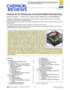
Nozzle-based 3D printing technologies The most widely used method for 3D printing relies on robotic control of scanning deposition nozzles in which 3D structures form in a layer‑by‑layer manner 85,98–101. Materials typically formulated from particulate and/or polymeric species with desired rheological behaviour serve as ‘inks’. Depending on the properties of the inks and the nature of the delivery process, these techniques can be further classified into two groups85,98,102: inkjet printing for liquid inks and microextrusion printing for viscoelastic inks (FIG. 1a). Inkjet printing, also known as drop‑on‑demand printing, exploits nozzles that use thermal or acoustic processes to deliver liquid droplets to desired locations on the substrate85,98,102–104. By contrast, microextrusion printing uses pressure-induced flow to form continuous filaments of material, often designed to solidify immediately or shortly after emergence from the nozzle tip. In both cases, proper materials formulation is essential. For inkjet printing, the challenges are in realizing high solid content for thick deposits, but at sufficiently low viscosity to allow droplet generation in a manner that also avoids clogging of the nozzles105. Although inkjet printing has widespread applications in forming 2D structures, 3D architectures can be difficult to form, partly owing to the uncontrolled flow of inks as they impinge on a structured surface106. By comparison, microextrusion printing offers far greater possibilities in 3D structuring owing to the broad range of ink designs and feature sizes. Microextrusion printers that offer modest (slightly sub-millimetre) resolution are now widely available in the form of commercial, user-friendly tools. In most cases, a printing head robotically controls the extrusion of a material ink onto a substrate, whereby a handling and dispensing system pneumatically or mechanically (with a piston or screw) controls the extrusion of materials in well-defined ambient conditions85. Recent research establishes methods for fabricating sophisticated 3D mesostructures with microscale resolution in a broad range of materials, including concentrated colloidal107, nanoparticle108, fugitive83,109 and polyelectrolyte110 inks. Main areas of current interest are in conductive and biomaterial inks because of their relevance in key applications, from solid-state lighting and wearable devices to tissue scaffolds and regenerative medicine. The following subsections highlight some of the latest progress.
2 | ARTICLE NUMBER 17019 | VOLUME 2
www.nature.com/natrevmats . d e v r e s e r s t h g i r l l A . e r u t a N r e g n i r p S f o t r a p , d e t i m i L s r e h s i l b u P n a l l i m c a M 7 1 0 2 ©
REVIEWS a 3D printing techniques Inkjet
Microextrusion Loading Switch Nozzle Nozzle
b Silver interconnects in a LED array
c Silver antenna on a hemispherical surface
d 3D silver helices and butterfly shapes
500 μm
200 μm
1 mm
1 cm
e 3D structures of liquid metal EGaIn
f Quantum-dot LEDs LED components
3D printing process
500 μm
500 μm
1 cm
500 μm
Nature Reviews illustration | Materials Figure 1 | Nozzle-based 3D printing technologies and applications in conductive structures. a | Schematic of nozzle-based inkjet (left) and microextrusion (right) printing techniques. Inkjet printing usually relies on thermal or acoustic processes to deliver liquid droplets to desired locations on a substrate. Microextrusion printing uses pressure-induced flows to form continuous filaments of material, often designed to solidify immediately or shortly after emergence from the nozzle tip. b | 3D silver interconnects between an array of microscale light-emitting diodes (LEDs). c | A 3D silver antenna printed onto a hemispherical surface. d | 3D silver helices and butterfly shapes. e | 3D structures printed with the liquid metal EGaIn. f | Schematic illustration of quantum-dot LED components and an optical image acquired during 3D printing of this multimaterial structure. Panel b is adapted with permission from REF. 70, AAAS. Panel c is adapted with permission from REF. 79, Wiley-VCH. Panel d is adapted with permission from REF. 80, National Academy of Sciences. Panel e is adapted with permission from REF. 82, Wiley-VCH. Panel f is adapted with permission from REF. 84, American Chemical Society.
3D printing with conductive inks. One notable ad vance70,79,80 involves highly concentrated silver nano particle inks (>70 wt% Ag) for electrically conductive filaments in 3D arrangements (FIG. 1b,c). The viscoelastic properties enable self-supporting structures, such as the arc-shaped features in FIG. 1b. Thermal annealing (for example, at 150–500 °C) performed after printing by convective heating 70 or during printing by heating with a focused laser beam80 can substantially improve the conductivity and the mechanical properties70. As shown in FIG. 1d, 3D helical coils and butterfly shapes can be formed by heating during printing 80. Electrically functional devices, such as 3D spanning interconnects in arrays of microscale light-emitting diodes (FIG. 1b) and hemispherical antennas (FIG. 1c), suggest broad utility in electronics and optoelectronics70,79. NATURE REVIEWS | MATERIALS
Other strategies use liquid-metal inks in the form of binary eutectic alloys of gallium and indium (EGaIn)81–83. EGaIn is a low-viscosity liquid at room temperature (with a melting point of ~15.7 °C). An ultrathin (~1 nm) passivating layer of gallium oxide forms immediately on exposure to air, thereby preventing spontaneous flow in ambient conditions81. As a result, at modest pressures (1 cm and >10 cm3 in volume) artificial tissues with embedded vessels (