A doubler circuit has been designed using a new planar diode layout, which ... diodes is about as large as is believed optimal for this frequency band. Design of ...
Tenth International Symposium on Space Terahertz Technology, Charlottesville, March 1999
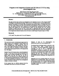
PROGRESS IN PLANAR DIODE BALANCED DOUBLERS T.W. Crowe and W.L. Bishop N.R. Erickson Dept. of Physics and Astronomy Dept. of Electrical Engineering. University of Virginia University of Massachusetts Charlottesville, VA 22904 Amherst, MA 01003
R.P. Smith and S.C. Martin Jet Propulsion Lab 4800 Oak Grove Pasadena, CA 91109
Abstract New developments in higher performance planar diode balanced doublers are reported. These include higher output power, higher efficiency, wider bandwidth, and simpler, more reliable construction. An output power of 80 mW was produced at 140 GHz using a new planar diode array designed to handle very high power. An efficiency of 25% was achieved at 270 GHz with 14 mW output. A wideband doubler has been designed which is extremely simple and easy to assemble, using a new planar diode with on-chip matching. All of these new designs are mechanically improved and should survive cooling to 80K. On those devices where tests have been made, the efficiency at 80 K improves by 30-36% relative to the room temperature value.
Introduction In work reported last year [1], a wideband fixed-tuned balanced doubler was described using planar diodes with typically 26% efficiency over the band 130-165 GHz. This doubler used an array of four diodes and worked best at 120 mW input power. In this new work, the same basic doubler circuit has been duplicated and improved in a number of ways. A new six diode array has been used in the doubler, and while not tested over any bandwidth, has produced a record high power. A similar circuit has been used with a four diode array in the 270-340 GHz band and works well, with very high efficiencies at 270 and 330 GHz. A cascaded pair of these doublers has been tested over a 5% bandwidth with good results. The general layout of a planar balanced doubler is shown in Figure 1. Output
Input Matching
Gold Ribbon
Waveguide Matching Section
Input Planar Coax DC Bias diode Matching Filter Section Figure 1. Balanced doubler using planar diode array, in a generic form. This circuit shows the essential elements and does not represent any real circuit.
475
Tenth International Symposium on Space Terahertz Technology, Charlottesville, March 1999
These circuits are now more easily and reliably assembled using wire bonding techniques and higher temperature solder. This enables them to work at hi gh power levels, where diode heating is a problem, without degadation. This assembly also reduces the strain on the diode at low temperature extremes. A 280 GHz planar diode doubler is being built for long duration space flight use in the Microwave Instrument for the Rosetta Orbiter (MIRO), a mission to a comet. A doubler circuit has been designed using a new planar diode layout, which incorporates output impedance matching into the diode itself. As a result the circuit is simpler and more readily assembled, and is predicted to work better, with very flat efficiency over a 20% band. Improved methods of assembly Early versions of these planar diode doublers followed closely upon their whisker contacted predecessors, using coaxial pins connecting the center pad of the diode to the output circuit. This makes it easy to produce a wide range of impedances but leads to a type of construction in which three solder joints must be completed at once. It is very difficult to be sure that all points are really soldered properly. In addition the rather stiff center pin is strong enough to break the diodes if it flexes, and this usually happens to some extent in cooling to 80K. This method of construction has been improved in some designs by replacing the coaxial circuit with a quartz substrate microstrip circuit, [2,3] which reduces the strain but still presents some assembly difficulties. Present designs use a thin ribbon to connect to the diode so that strain is not a problem. In addition, it is easy to thermo-compression bond this wire to the diode if a pure gold ribbon is used, and this eliminates the potential problem with one solder joint. These solder joints can be a problem as was seen on one doubler that failed after being driven at 250mW for three days. The solder joints were found to be severely degraded, apparently because the diodes ran so hot that the indium solders used either oxidized or melted. After experiencing the high power failure, subsequent doublers have been built with bonded ribbons and a higher melting temperature solder (MP 149C) between the diode and the waveguide wall. High power diodes In an effort to build a diode able to handle very high power, a six anode diode was designed for use in the 150 GHz range. The diode was intended as a replacement for the existing four anode diode, in a chip with the same overall length. A combination of impedance matching and moding concerns makes it essential that the waveguide height used with these diodes not be too large, and the 0.66 mm height used with the existing diodes is about as large as is believed optimal for this frequency band. Design of such a diode is not as easy as for four anode devices because the space available for the diodes becomes smaller and the parasitic elements more important. This design was also intended to improve the impedance matching to the diode over a wide band. The simplest design, with 6 anodes spaced nearly evenly across the waveguide, showed serious problems
476
Tenth International Symposium on Space Terahertz Technology, Charlottesville, March 1999
because the input power divided unevenly between the diodes, while the output coupling showed even larger variations. The cure for this problem is to space the diodes much more closely, since the parasitics depend on their location within the waveguide, and also to space the diodes unevenly. The general approach to the design was to place all of the diodes near the waveguide wall, where it would be easier to heatsink them, and then to adjust the spacing until all diodes coupled equally to the external circuit. This results in very little space for the ohmic contact pads and special problems in the fabrication of the diodes. The method of design was to simulate the circuit of the input waveguide (split in half due to symmetry) in HFSS [4] with an input waveguide port, an output TEM port, and 3 diode ports, and to attempt to achieve a uniform impedance environment for the three diode ports. Simulations were performed for both the input and output frequencies. Testing the design required terminating the diode ports in this simulation with actual varactor impedances and determining how uniformly the power split to the ports. These impedances were determined using a nonlinear simulator to optimize a single diode circuit at the expected drive level [5]. It is important to not compare the S parameters into 50 CI 500 comparisons can be very misleading since the diodes are so reactive, and the port power balance is very sensitive to capacitance. In general these simulations showed that the output frequency presents the most difficult problem, and that the variation in power becomes worse with increasing frequency. There is no really perfect solution, but a power imbalance of 0.5 dB is certainly not serious, and simulations seem to indicate that even a 1 dB imbalance has no major consequences. The one thing that is difficult to simulate is the division of bias voltage across the diodes when the circuit impedances are not matched. All simulations assumed equal bias voltage on each anode. The final design uses a relatively long contact finger to the first diode on each side, with this finger length decreasing for the second diode and even more for the third. The remaining space to the center pad is taken up with a high impedance line to add as much inductance as possible. This diode was originally laid out for fabrication at JPL, where the diode process is able to make almost exactly the designed shape. However, the diodes made at JPL had relatively poor properties, and while they worked in the doubler and could handle high power, the efficiency was only 23%. The design was not so compatible with the INa process, because the finger length for the innermost diode is too short for the UVa surface channel etch process, and also because the optimized ohmic pad sizes are too small as well. Therefore, the diode that eventually was produced was not exactly the optimized design, but was believed to be close enough to try out the idea. These diode layouts are shown in Figure 2. The diodes were successfully processed at UVa (batch SB8T1), but no DC parameters were available since the measured R s is too strongly influenced by heating effects. The diodes were installed into the wideband doubler designed for a 4 anode
477
Tenth International Symposium on Space Teralzertz Technology, Charlottesville, March 1999
er111--
7, a
Figure 2. Six anode diode designed for optimum use in the 140-170 GHz band (top), and the diode made at UVa as a compromise to utilize their fabrication process (bottom). Dimensions are in gm.
chip [1], since no doubler designed for these new diodes was available. The doubler was tested at input frequencies between 70 and 85 GHz using high power IMPATT sources. The best performance in terms of circuit matching was seen at 70 GHz. At this frequency the input reflection was about 20%, while the source power was nearly 300 mW, so delivering sufficient power to drive the input was not a problem. The output match was optimized with a single Teflon quarter wave transformer in the output waveguide. The diode was installed into the circuit by bonding a gold ribbon to the diode center pad, and then soldering the diode outer pads to the waveguide walls with Indalloy #2 solder (MT 149C). The diode survived the full 300 mW input power available, with nearly 250 mW actually absorbed by the diode. The output power at this drive was 80 mW, and this power level was sustained for a period of 1 day. In this time the diode IV curve changed slightly, but showed no signs of leakage, which normally occurs if a diode is seriously overdriven. At a lower power of 210 mW absorbed, and 70 mW output, the test was carried out for 1 week, so it appears that this is a safe operating power. The peak efficiency occurs at 150 mW absorbed power, where the efficiency, corrected for input mismatch, is 35%. This efficiency is typical of that of other good diodes produced at UVa, and tested at similar frequencies, although somewhat lower than the best (40%). Therefore, it seems that the power combining in the three series diodes is fairly efficient, and that the fabrication compromises are not too serious. However, all of the problems are expected to become worse at the higher end of the design band near 170 GHz, and no tests have been done here since the diode matches the existing circuit so poorly. This doubler was tested at —80 K with only 215 mW input power (196 mW absorbed) due to the loss of the stainless steel waveguide required to thermally isolate it from the room temperature source. At room temperature before cooling the output power was 64 mW, while the cold output power was 85mW, an increase of 33%. The cold efficiency (corrected for input mismatch) is 43%.
478
Tenth International Symposium on Space Terahertz Technology, Charlottesville, March 1999
High efficiency doublers for 270-340 GHz A similar doubler for twice this frequency has also been completed, using four anode diodes. This more conservative design requires tuning the output backshort in order to cover the full 270-340 GHz band, but the bandwidth is —20 GHz with fixed tuning. It also uses a 2 mil wide gold ribbon for strain relief in the connection between the planar diode and the output waveguide. At room temperature the efficiencies achieved with this doubler are much better than with the previous model [6]. The best results at 270 GHz are 14 mW output at an efficiency >25% using a diode fabricated at JPL, and at 330 GHz, 7.0 mW output at an efficiency of 18% using a UVa diode. It works well at 80K, with an efficiency improvement (using the JPL diode) of 35% relative to the room temperature value. The bandwidth of this doubler is not optimized for fixed tuning but shows the potential for wideband operation. Figure 3 shows the power output with a Gunn oscillator pump (without an isolator between the Gunn and doubler) over a moderate band. In this test, a Teflon tuner was added in the input waveguide very close to the diode to improve the match. While there is a lot of power ripple due to the interaction with the Gunn, the power at the peaks of the ripple is large and the bandwidth is broad enough to be quite useful. Presumably the ripple would go away with an isolator in the circuit, but this was not attempted because the doubler works best at the highest input power available (-50 mW), and the loss of the present isolators drops the power to a suboptimal level. 12 - Gunn oscillator driving doubler directly, doubler fixed tuned
8
0. 0. 4
0 250
270
260
280
Output Frequency (GHz)
Figure 3. Output power from doubler and Gunn with no isolator, and fixed doubler tuning. The power ripple is due to the interaction between the Gunn oscillator and the doubler input match.
We have cascaded two of these doublers to produce a 330 GHz source. This source produced a peak power of7.0 mW, and a minimum power of 5 mW over a band of 325-335 GHz, with an input power of 130 mW, all at room temperature. The diodes in both doublers were from UVa (batches SC6T6 and SB3T2). Figure 4 shows the performance measured over an extended band using higher input power at some of the
479
Tenth International Symposium on Space Terahertz Technology, Charlottesville, March 1999
extreme points. Despite the lack of an isolator between doublers, there is little ripple in the output power over most of the band, showing that over a limited band. doublers can be matched quite well. However, this is much more difficult over a wider band. 8
6 66
ci-
4
2 Input pcweer 130-170 tviv tnterstage isokator
320
325
340
330
Output Frequency (GHz)
Figure 4. Cascaded doubler performance at room temperature with mechanical tuning fixed. No isolator was used between the doublers. The match between stages is good enough over the midband that the power ripple is minimal.
Wideband doubler using improved diode layout To make the assembly of these doublers easier, we have designed a new set of planar doubler diodes intended for use near 280 GHz. These incorporate on-chip vvideband matching to optimally couple into a circuit having relatively high impedance. This potentially eliminates the need for any microstrip circuit, since the output circuit can be just a gold ribbon connecting to the output waveguide. The starting point for this work was the diode mask designed at UMass a few years ago and fabricated at UVa as the successful batch SB3T2. This layout produces a fairly serious power imbalance at frequencies above 300 GHz, and requires that the first section of the output matching circuit have a low impedance for matching over a wide band. The low impedance line is needed to add capacitance to the output to compensate for the excess inductance in the diode. Reducing the diode inductance is not practical because the input matching depends on a large inductance. It was found that simply adding some metal area to the diode center pad is all that is required to eliminate the low impedance line, but the method of adding this area is critical because it seriously affects the parasitics for the individual diodes. In particular, adding metal which closely approaches the small midpad in the diode pair causes the inner diode's parasitics to increase, so a pad was developed which flares out as a trapezoid as it leaves the critical region. In addition, the other side of the pad was also enlarged slightly. In principle, even more capacitance may be added as a stub line on this side, but it was not found to work well in practice. The final layout is shown in Figure 5.
480
Tenth International Symposium on Space Terahertz Technology, Charlottesville, March 1999
End pad (solder to wall) Ohmic pad
457
Center pad
Figure 5. Original SB3T2 diode layout (left) and the new design with better output matching. Diode locations are shown by small circles. Dimensions are in gm.
All of this design was done with the assumption of a GaAs thickness of 37 pm. This thickness makes it easy to handle the diodes and appears to have only a minor effect on the circuit bandwidth. The dominant effect of varying substrate thickness is to change the optimum capacitance of the diode for a given circuit design. If diodes are made in a few capacitance values it should be possible to correct for errors in thickness, or vice versa. With the added area, the diode power match was not seriously affected, and in fact the outer diode was still found to have the larger parasitic capacitance so its outer pad was moved out to the very edge of the waveguide. All of this design work was done in much the same way as for the six anode diode described above, while investigating the diode match into a nearly ideal circuit. No full circuit optimization is practical, due to its complexity, until one arrives at a final diode design. After the diode was designed, the optimized output impedance was quite high, and best coupled as directly as possible into waveguide, which is better suited for high impedance circuits than TEM media. This was facilitated by the optimized input circuit, which favored placing the diode extremely close to the waveguide backwall. The required connecting wire turned out to be quite short, only slightly longer than that required to extend from the diode to the far wall of half height output waveguide. Thus this wire becomes more of an interconnection than a circuit element. The output waveguide circuit was optimized and a two section step transformer to full height was placed at an optimized distance from the transition. The final circuit was quite simple, yet the predicted output match shows a 14 dB return loss over an 18% bandwidth. Bias to the diode is still required, but without the need for any other circuitry, the bias may be de-coupled from the output by bonding the ribbon to a capacitor at the far wall of the waveguide. The circuit is shown in Figure 6.
481
Tenth International Symposium on Space Terahertz Technology, Charlottesville, March 1999
■■■••■•••■•■•■•■,,,,
Output Waveguide
-■
Kii, yoass copz.,citc-
Scow :hc^re : i bor......., • ;; ) ccnnec :tic wo,eg...7ces ''''' '