Journal of Optoelectronics and Advanced Materials Vol. 7, No. 1, February 2005, p. 297 - 300
PROPERTIES OF REACTIVE O2 ION BEAM SPUTTERED TiO2 ON Si WAFERS S. Ulucan, G. Ayguna, L. Ozyuzer*, M. Egilmez, R. Turana Department of Physics, Izmir Institute of Technology, Urla, 35430, Izmir, Turkey Department of Physics, Middle East Technical University, 06531, Ankara, Turkey
a
TiO2 thin films were deposited on silicon (100) p-type wafers, using the reactive ion beam sputtering method in high vacuum as an alternative to conventional Argon ion beam sputtering in an O2 environment. Oxygen ions with 1000 eV energy were formed in a thruster and bombarded a high purity Ti target. The molecules of TiO2 were deposited on a Si (100) wafer at various substrate temperatures. The structural and optical properties were analyzed using Fourier Transform Infrared Spectroscopy in the range of 400–4000 cm-1. An ellipsometer was used to measure the thickness and refractive index of the deposited films. In order to determine the dielectric constant and capacitance of the deposited TiO2, the electrical properties were studied using an MOS capacitor. The effects of substrate temperature and deposition time on the dielectric properties of TiO2 are discussed.
(Received December 9, 2004; accepted January 26, 2005) Keywords: TiO2, Ion Beam Deposition, CMOS
1. Introduction Microelectronics technology is based on silicon and silicon dioxide (SiO2) thin films. These are especially useful as gate oxides in metal-oxide-semiconductor field effect transistors (MOSFETs). Even though various techniques [1] are still being researched to obtain high quality thin SiO2 layers for CMOS technology, the downsizing of devices approaches the physical limits of SiO2. There have been extensive efforts to form thin dielectric insulators as an alternative to SiO2 [2]. Titanium dioxide (TiO2) is a promising material to replace SiO2 thin films, due to its high relative dielectric constant of up to 100 [3,4]. In addition to the significance of TiO2 in microelectronics, its high optical transmittance and high refractive index make it applicable in many areas such as coatings, optical filters, integrated optical chemical sensors, optical waveguides etc. [3,5]. The crystal structure of TiO2 is important for microelectronics applications. The amorphous state is used for optical coatings, while rutile TiO2 is used for dielectric layers due to its high dielectric constant and the anatase phase is used for dye-sensitized solar cells due to its higher band gap [6]. There are several methods for producing TiO2 thin films. These are metal-organic decomposition (MOD) [4], ultraviolet-assisted injection liquid source chemical vapor deposition (UVILS-CVD) [5], plasma-enhanced chemical vapor deposition (PECVD) [7], low-pressure chemical vapor deposition (LPCVD) [8] and reactive sputtering in high vacuum [9]. In this study, the fabrication of TiO2 films on Si substrates by reactive ion beam deposition using oxygen ions in high vacuum has been accomplished. To the best of our knowledge, this is the first attempt to grow thin films of TiO2 using reactive oxygen ions.
*
Corresponding author:
[email protected]
298
S. Ulucan, G. Aygun, L. Ozyuzer, M. Egilmez, R. Turan
2. Experimental details In this study, the TiO2 films were grown on p-type Si (100) wafers with a resistivity of 1517 cm, by reactive sputtering using O2 ions. The Si wafers were cleaned as described elsewhere [1]. The surfaces of wafers were hydrophobic after an HF dip, showing that the native oxide layer was removed from the surface. The cleaned substrates were loaded into the ion beam deposition system. The base pressure of the chamber was kept below 10-6 Torr with a turbomolecular pump. The ion source was an Advanced Energy MCIS 12 closed drift end Hall type thruster, with a 12 cm beam diameter [10]. During the deposition, the pressure was 1.0x10⁻³ Torr, and ion beam current density was 1.0 mA/cm2. High purity (99.2%) Ti plates were used as targets in this study, and they were etched with Ar ions in order to remove the oxide layer on the target before each deposition. O2 ions formed using a 1000 eV accelerating voltage were directed onto the Ti target, which was located at an angle of 45o with respect to incident ions. Samples were prepared at room temperature, 200 oC and 300 oC for 20, 40 and 60 minutes deposition times, by using a heater placed outside the chamber, which was well contacted to the substrate flange. The temperature was controlled with a K-type thermocouple, placed on the surface of the wafer. The structural and optical properties of the grown films were analyzed using Fourier Transform Infrared Spectroscopy (FTIR), (Nicolet Magna IR Spectrometer 550) in the range 400 4000 cm-1. Diffuse and reflectance techniques were used for FTIR measurements. The resolution was 4 cm-1 and the scan number was 256 for each run. For the structural characterization, SEMEDX analysis was performed with a Philips X’pert FEG. The thickness, d, and refractive index, n, of the deposited oxide layers were determined using an ellipsometer, ( = 632.8 nm). The electrical characterization of the layers was carried out using MOS capacitors with evaporated Al gate electrodes. The rear sides of the wafers were HF-cleaned, followed by Al metallization. The dielectric and electrical characteristics of the layers were studied using Capacitance-Voltage (C-V) and Conductance-Voltage (G-V) measurements. The oxide charge Qf was evaluated from the flat band voltage, Vfb, of the high-frequency (100 kHz) C-V curves. 3. Results and discussion
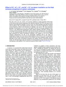
20 min 40 min 610 cm
60 min
-1
Absorbance (a.u.)
Absorbance (a.u.)
Fig. 1a presents the FTIR spectroscopy of samples prepared at room temperature for 20, 40 and 60 minutes. In the range 4000 to 2000 cm-1, no absorption peaks were found for any samples. Each graph has a main peak at about 610 cm-1, which is a characteristic peak of rutile TiO2 [5,11]. The intensity of the peaks at 610 cm-1 increased with increasing deposition time. A characteristic peak of the Si–O bond was also observed around 1080 cm-1, which shows that a SiO2 interface layer was formed between the TiO2 and the Si substrate. The intensity of this peak decreased with increasing deposition time, and interference fringes appeared.
room temp
200 o C
300 oC
610 cm
(b)
(a) 2000
1600
1200
800
-1
Wave Number (cm )
-1
400
2000
1600
1200
800
400
Wave number (cm-1)
Fig. 1. FTIR spectroscopy measurement results (a) 20, 40, 60 minutes at room temperature samples, (b) room temperature, 200 °C, 300 °C for 40 minutes samples.
Fig. 1b shows the FTIR spectroscopy of deposited TiO2 films on Si substrates at different substrate temperatures (room temp., 200 °C, 300 °C) for 40 min. In this figure, the same peaks related to the TiO2 and Si–O bond were also observed. All samples prepared at various temperatures
299
Properties of reactive O2 ion beam sputtered TiO2 on Si wafers
have peaks of TiO2 around 610 cm-1. The magnitude of peaks increased with increasing temperature, as is seen with increasing deposition time (Fig. 1a). The FTIR analysis established that the deposition time and temperature had the same effect on the growth of the TiO2 . Table 1. EDX, thickness and refractive index measurement results
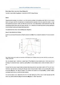
Room temp. 40 min 60 min 4.78 7.13 6.00 8.61 199.8 292.0 1.769 2.008
%Wt O %Wt Ti d( ) N
3 10
2 10
10 kHz capacitance 100 kHz capacitance 10 kHz conductance 100 kHz conductance
-9
0.0008
-9
200 °C 40 min 60 min 3.35 4.73 3.94 6.18 144.9 154.6 1.745 2.061
3 10
2 10
300 °C 40 min 60 min 3.87 10.44 3.63 3.19 154.7 153.0 1.305 1.783 10 kHz capacitance 100 kHz capacitance 10 kHz conductance 100 kHz conductance 0.0012
-9
-9
0.0008
0.0004 1 10
-9
1 10
-9
0.0004
(b)
(a) 0 -2
-1
0
Applied Voltage (V)
0
0 -2
-1
0
0
Applied Voltage (V)
Fig. 2. C-V and G-V curves at different frequencies (10 kHz and 100 kHz) a) Room temperature, 40 min sample b) 200 oC, 40 min sample.
EDX analysis indicated that the Ti weight ratio increased with deposition duration, for samples prepared at room temperature (Table 1). Extending the deposition times had a positive effect on the oxidization process of the Ti for the room temperature samples. EDX measurements showed that the oxidized Ti (TiOx) was stoichiometric for room temperature samples, while the stoichiometry was broken at higher substrate temperatures, i.e. 300 oC. Since EDX gives only rough estimates, an XPS study is under way. The thickness, d, and refractive index, n, values of TiO2 films are also shown in Table 1. As seen, the thickness of samples prepared at room temperature was greater than that of the higher substrate temperature ones. Expanding the deposition times resulted in increases of the thickness and the refractive index value of the TiO2 films. The refractive index approached the bulk value, which is 2.5 [5,12], when the deposition time was increased. The electrical properties of the grown films were studied using an admittance technique. Fig. 2 shows the typical high frequency (10 kHz and 100 kHz) Capacitance-Voltage (C-V) and Conductance-Voltage (G-V) curves of samples grown at room temperature and 200 oC. Although they exhibited the general characteristics of a MOS capacitor, a ‘leaky’ behavior is seen from these curves. The presence of the conductance peak in the G-V curves is, however, an indication that the device worked as a MOS capacitor in spite of the leakage. Upon comparison, the sample grown at room temperature is seen to have less leakage and a better quality than that grown at 200 oC. This is likely to result from the presence of a thin oxide layer between the substrate and the grown film at room temperature. As confirmed by the FTIR measurements, this SiO2 layer was not detected in the sample grown at 200 oC. The oxide thicknesses measured by ellipsometry, the dielectric constant and the fixed oxide charges determined from C-V measurements are given in Table 2. The oxide values extracted from the capacitance values measured in the accumulation regime are higher than that of pure εSiO2 (3.9εo) and smaller than that of εTiO2(80εo-100εo). This can be explained by two phenomena: the presence of a SiOx film between the TiO2 film and the substrate, and the possible non-stoichiometric structure of TiO2. We also see that the dielectric constant increased with substrate temperature, indicating either an improvement in the stoichiometry of the film or a decrease in the relative contribution of the
300
S. Ulucan, G. Aygun, L. Ozyuzer, M. Egilmez, R. Turan
interfacial SiOx layer. The FTIR and EDX results suggest that the increase in the dielectric constant with the substrate temperature was more likely to be connected to the absence of the SiOx layer at higher substrate temperatures. The oxide charges determined from the shifts of the C-V curves are within the acceptable ranges for device production. Table 2. Dielectric and electrical values of MOS capacitors
Room Temp, 40 min Oxide Thickness ( ) 199.8 Al gate area (m2 ) 1.13×10⁻⁶ 100 kHz frequency Cacc (F) 2.7×10⁻⁹ 5.39 calc 10 kHz frequency Cacc (F) 3.16×10⁻⁹ 6.31 calc Fixed Oxide Charges (Qf) for 100 kHz 4.2×10¹¹ (cm-2 )
200 oC, 40 min 144.9 3.12×10⁻⁷ 2.13×10⁻⁹ 11.19 3.29×10⁻⁹ 17.28 -1.0×10¹²
In conclusion, the reactive ion beam sputtering method has been successfully used to deposit TiO2 films on Si substrates. The deposited TiO2 films were examined by FTIR, EDX, ellipsometry and electrical measurements using MOS capacitors. The analysis showed that the properties of TiOx films formed on Si depend on the deposition conditions. The presence of a SiOx layer between the TiO2 film and the Si substrate was identified by FTIR spectroscopy at room temperature. However, this layer was not detected at higher substrate temperatures. In order to obtain more accurate structural compositions as a function of depth, XPS measurements are in progress.
Acknowledgements This research is partially supported by TUBITAK (Scientific and Technical Research Council of Turkey) project number TBAG-2031. L.O. acknowledges support from the Turkish Academy of Sciences, in the framework of the Young Scientist Award Program. References [1] G. Aygun, E. Atanassova, A. Alacakir, L. Ozyuzer, R. Turan, J. Phys. D: Appl. Phys. 37, 1569 (2004). [2] E. Atanassova , T. Dimitrova, Handbook of Surfaces and Interfaces of Materials, ed. H.S. Nalwa Vol. 4, (2001). [3] H. Shin, M. R. Guire, A. H. Heuer, J. Appl. Phys. 83, 3311 (1998). [4] H. Fukuda, S. Namioka, M. Miura, Y. Ishikawa, M. Yoshino, S. Nomura, Jpn. J. Appl. Phys., 38, 6034 (1999). [5] J. Y. Zhang, I. W. Boyd, B. J. O’Sullivan, P. K. Hurley, P. V. Kelly, J. P. Sénateur, J. Non-Cryst.Solids 303, 134 (2002). [6] E. Halary, E. Haro-Poniatowski, G. Benvenoti, P. Hoffman, Appl. Surf. Sci. 168, 61 (2000). [7] H.-K. Ha. M. Yoshimoto, H. Kounima, B.-K. Moon, H. Ishiwara, Appl. Phys. Lett. 68, 2965 (1996). [8] N. Raush, E. P. Burte, J. Electrochem. Soc. 140, 145 (1993). [9] J. Szczyrbowski, G. Bräuer, M. Ruske, J. Bartella, J. Schroder, A. Zmelty, Surf. Coat. Tech. 112, 261 (1999). [10] Advanced Energy Industries Inc., 1625 Sharp Point Drive Fort, Collins, CO 80525 USA. [11] V. G. Erkov, S.F. Devyatova, E. L. Molodstova, T. V. Malsteva, U.A. Yanovskii, Appl. Surf. Sci. 166, 51 (2000). [12] X. Wang, H. Masumoto, Y. Someno, T. Hirai, Appl. Phys. Lett. 72, 25 (1998).