Oct 27, 2009 - The DUT was prepped for test by Timothy Irwin and James Forney by first delidding the package and then soldering the DUT to a printed circuit ...
Pulsed Laser Single-Event Transient Testing of the M.S. Kennedy 5900RH Radiation Hardened ULDO Adjustable Positive Linear Voltage Regulator
J. A. Pellish(1), S. Buchner(2), D. A. Batchelor(1), J. D. Forney(3), and C. M. Seidleck(3)
NASA Goddard Space Flight Center Code 561.4, Radiation Effects and Analysis Group 8800 Greenbelt RD Greenbelt, MD 20771
27 October 2009
(1) NASA Goddard Space Flight Center, Greenbelt, MD USA (2) Global Strategies Group, Crofton, MD USA (3) MEI Technologies, Inc., Greenbelt, MD USA
Table of Contents 1.
Introduction .......................................................................................................................................... 1
2.
Devices Tested ...................................................................................................................................... 1 2.1
MSK5900RH Background .............................................................................................................. 1
2.2
Device Under Test Information ..................................................................................................... 3
3.
Test Setup ............................................................................................................................................. 3
4.
Test Description .................................................................................................................................... 4 4.1
Irradiation Conditions ................................................................................................................... 4
4.2
Test Parameters and Bias Conditions ........................................................................................... 5
5.
Results ................................................................................................................................................... 5
6.
Conclusions and Recommendations ..................................................................................................... 6
7.
Run Log.................................................................................................................................................. 8
8.
References ............................................................................................................................................ 9
ii
1.
Introduction
The ultra-low dropout (ULDO) positive adjustable voltage regulator, 5900RH, from M.S. Kennedy (MSK) was tested for analog single-event transients (ASETs) with a pulsed laser source at the Naval Research Laboratory (NRL) on 27 October 2009. The output of the voltage regulator was monitored for ASETs and the device current supply was monitored for high-current events.
2.
Devices Tested
2.1
MSK5900RH Background
The MSK5900RH is a hybrid integrated circuit adjustable voltage regulator, which contains controller circuitry that governs a power PNP bipolar transistor. The controller circuitry, manufactured by Linear Technology, is the LT1573 low dropout PNP regulator driver. The LT1573 is available as an adjustable regulator with an output range of 1.27 V to 6.8 V and with fixed output voltages of 2.5 V, 2.8 V, and 3.3 V; the adjustable regulator is used in the MSK5900RH. The block diagram of the LT1573 is shown in Figure 1, a picture of a delidded MSK5900RH shown in Figure 2, and a die micrograph of the LT1573 shown in Figure 3. The regulating loop consists of a 1.265 V reference, an error amplifier, a Darlington driver and an external PNP pass transistor. The LT1573 is the primary target for pulsed laser ASET testing.
Figure 1: LT1573 block diagram taken from the datasheet. A functional description can be found in the LT1573 datasheet.
1
PNP
LT1573 Figure 2: Photograph of delidded MSK5900RH. The external PNP and LT1573 low dropout PNP regulator driver are shown with text labels and arrows. Note the scale bar in the lower right-hand corner of the image. This is the orientation of the part as the laser sees it. The smallest resolvable feature size is 40 µm.
Figure 3: LT1573 photomicrograph. The location of the LT1573 within the MSK5900RH case is shown in Figure 2. The image has been rotated to match the orientation in Figure 2, so the micrograph legend is inverted in the top left corner. The smallest resolvable feature size is 1.25 µm.
2
2.2
Device Under Test Information
One device was exposed to the pulsed laser beam at the NRL. The device lot date code was 0703. The DUT was packaged in a hermetically-sealed 12-pin flatpack with formed leads suitable for surface mount applications. The DUT was prepped for test by Timothy Irwin and James Forney by first delidding the package and then soldering the DUT to a printed circuit board (PCB). This ASET test is applicationspecific and requires a custom output filter circuit for the voltage regulator, which is described in the following section. Table 1 lists the pertinent information about the DUT. Table 1: MSK5900RH Sample Information
Part Number:
MSK5900RH (SMD: 5962R0522001KSX)
Manufacturer:
M.S. Kennedy (LT1573 driver manufactured by Linear Technology)
Date Code:
0703
Additional Case Markings: 0196, 51651
3.
Quantity Tested:
1
Part Function:
Voltage regulator
Part Technology:
Bipolar hybrid integrated circuit
Package Style:
12-pin flatpack
Test Setup
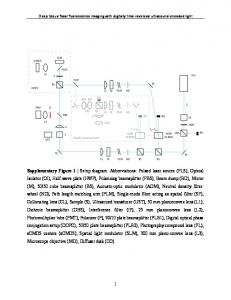
The test setup is shown in Figure 4 and consists of laptop running LabVIEW for instrument control and data capture, a Tektronix 4104 mixed-signal digital storage oscilloscope (1 GHz, 5 GS/s), Hewlett Packard 6624 4-channel power supply, and two Tektronix P5050 500 MHz passive voltage probes (10 MΩ, 11.1 pF). The DUT was placed on a custom PCB that included a filter circuit. The PCB schematic and corresponding parts list are shown in Figure 5.
GPIB
Computer 1
Digital Storage Oscilloscope
Voltage Probes
DUT PCB
4-channel Power Supply GPIB Figure 4: Block diagram for test setup of the MSK5900RH.
3
Apply power supply here
Load resistor added here
Apply load and measure transient here
Figure 5: Custom PCB and parts lists for filter circuit. Note that ferrite bead B1 has been removed from the schematic, though it is still listed in the parts table. The only modification required for this test was the addition of a resistor to the output (T1/T6). This resistor, either 100 Ω or 18 Ω, was necessary to set the proper circuit load since the loads required for this design fell below the limits of the available electronic load. The input voltage was set to 5 V and the output to 2.5 V by using resistors R1 and R2 into the feedback port at pin 7.
Two voltage probes were attached to nodes T1 and T6, fed back to the oscilloscope, and connected to analog channels 1 and 2. Channel 1 was set to trigger on positive transients and channel 2 was set to trigger on negative transients, thereby eliminating the need to repeat irradiation scans with the laser. Sampling was done at 100 ns/point (10 MS/s), which is sufficient for the size of the measured transients. The initial test plan called for the oscilloscope to be DC-coupled to the regulator filter output (T1/T6), but the small transient amplitude necessitated an AC-coupled setup to remove the DC offset and increase the vertical resolution on the oscilloscope.
4.
Test Description
4.1
Irradiation Conditions
The tests were performed at the Naval Research Laboratory (NRL) using their single-photon absorption (SPA) setup. This system has been discussed in several refereed publications and will not be covered in detail [1-3]. The laser wavelength is 590 nm, has a pulse width of approximately 1 ps, and is operated at a 1 kHz repetition rate. A 100x microscope objective was used to focus the laser beam down to a full width half maximum (FWHM) Gaussian spot of approximately 1.2 µm. Throughout the test, the pulse intensity, as measured on a NRL oscilloscope, was kept at 26.6 mV – the laser was also passed through a neutral density filter with an optical density of 0.6 1. Given these conditions, the resulting charge 1
There are many ways to make an estimate of the equivalent LET of the laser pulse when conducting SPA. For the present experiment, this was not the goal since the investigators were just evaluating a conservative scenario. The term “worst case” has been avoided since it is difficult to confirm such a conjecture in an absolute sense The pulse “energy” of 26.6 mV through OD-0.6 is an LET > 100 (MeV·cm2)/mg. 4
generation in the sensitive silicon layer beneath the back end of line (BEOL) material stack is sufficient to conduct a conservative ASET analysis.
4.2 Test Parameters and Bias Conditions
The laser was focused onto the LT1573 die and scanned across the surface to produce transients on the filter output. This was done for two different load conditions, which are detailed in Table 2. This was an application specific test and the only variable was the load current. Transients were captured at the minimum load value of 25 mA and the maximum load value of 138 mA; all other values remained fixed during testing. The resistors used between nodes T1 and T6 in Figure 5 resulted in a slight deviation from the ideal load values of 24 mA and 133 mA; there was a 4% positive deviation in each case. Before performing the experiment at the NRL, we evaluated Joule heating by measuring the case temperature of the device under test with a thermistor while passing the maximum application current, 138 mA, through the device under test. No increase in case temperature was observed, which is not surprising given the small current loads required and the thermal mass of the metallic flatpack. Table 2: Circuit Load Conditions
DUT Number
Laser Pulse † Voltage (mV)
SN1 SN1
26.6 26.6
Neutral Density Filter Optical Density 0.6 0.6
Load Current (A)
Input Voltage (V)
Output Voltage (V)
0.025 0.138
5.0 5.0
2.5 2.5
- The relative humidity throughout the test was constant at 45%. - The ambient temperature was constant at 22° C. - The load currents were both 4% above the ideal loads of 24 and 133 mA. † Note that laser pulse voltage is a relative measure of the laser pulse energy and depends upon an independent calibration to calculate the pulse energy.
5.
Results
The laser was scanned across the LT1573 die for each of the current load conditions specified in Table 2. Several areas on the die were capable of producing transients at the output of the filter and were recorded by the oscilloscope. In general, the larger load of 138 mA produced more transients, though the smaller load of 24 mA produced wider transients. These results are summarized in the plot shown in Figure 6. Four representative transients are shown in Figure 7. These represent two of the largest and two of the widest waveforms captured, which are meant as an example and not an exhaustive display. The transients have a similar, bipolar shape, though the transients in Figure 7a each have a voltage spike at the peak of the transient, making the amplitude seem larger even though this spike is very short in duration. One key feature to note is that the transient widths shown in Figure 6 are measured at 10% of the transient peak. Figure 7a clearly shows a narrow spike at the transient peaks, which in the automated data reduction process is logged as the transient peak and thereby determines at which points the transient width gets measured. While mathematically accurate, this scheme made it difficult to evaluate the transients at full width half maximum since the routine was then essentially calculating the width at the peak of the transient sans the spike. Though not true for all the transients captured, this common data artifact results in artificially short transients, which is why the routine was modified to calculate the width at 10% of the peak value.
5
Figure 6: The transient peak is largest voltage deflection from the mathematical baseline voltage, measured during the pretrigger phase. The width is calculated at 10% of the transient peak. The device under test appears to be more sensitive for the larger load of 138 mA than at 25 mA. At 25 mA, wider transients were measured than at 138 mA, though many of the transients were very short and captured at the limit of the sampling resolution for this experiment.
(a) Sample of largest peaks
(b) Sample of largest widths
Figure 7: Four representative transients from each of the circuit load conditions listed in Table 2. The transient width measurements shown in Figure 6 are measured at 10% of the peak voltage deflection. This was done because of the spikes at the transient peaks, visible in (a), were distorting FWHM calculations. If the transients were measured at FWHM, the analysis routine would have been measuring the transient width at the peak of the actual transient, artificially shortening the reduced value. The transients at the lower load value are wider than the transients at the higher load value.
6.
Conclusions and Recommendations
The MSK5900RH and accompanying filter tested here showed transients less than ±50 mV in amplitude for both load conditions under the same input and output bias conditions. The transients widths, measured at 10% of the peak voltage, ranged from a few tens of microseconds to several hundred microseconds. The transients at the smaller load value had scattered widths and generally a smaller
6
amplitude than the transients recorded at the higher load value, which were clustered around an average of 86 µs. No high-current events were observed. Based on the pulsed laser test results, the MSK5900RH is recommended for use in NASA/GSFC spaceflight applications, but may require mitigation (i.e., filter) techniques like those demonstrated in this report.
7
7. Run Log Table 3: Run log for ASET transient experiment on the MSK5900RH
Run #
1-2
3
Part Type
5900
5900
Time
09:31
10:23
Pulse Voltage (V)
2.66E-02
2.66E-02
ND Filter (OD)
6.00E-01
6.00E-01
Load (A)
2.40E-02
1.33E-01
Target
LT1573 dice
LT1573 dice
4-5
5900
11:06
2.66E-02
0.6
1.33E-01
LT1573 dice
6
5900
11:12
2.66E-02
0.6
2.40E-02
LT1573 dice
Comments
Present: Jonny, Jim, Dave, Megan, Steve, and Dale. Test set is at room temperature and will remain that way. No transients observed with these conditions. Switched DPO to AC-coupled from DC-coupled and re-centered the transient capture window. Temp: 71.6 deg, 45% RH.
Starting DAT #3 file. #2 contains the light switching transients. Pulse energy increased to 31 mV during the course of this exposure. Reset to 26.6 mV. Captured transients from turning light on and off. Shielded the DUT after resetting the laser pulse voltage Reset scale to 100 us/div and 20 mV/div and are able to see transients. Transients are about 20 mV in amplitude (pos and neg) and about 200-300 us in length. Largest was 30 mV in amplitude. Will actively rescale the scope time and voltage bases if necessary throughout the run. With the smaller load, the transients stayed about the same. The sensitive transistor seems to be located on an input/output. Transients are still small, about 30 mV and 200 us in length.
8
8.
References
[1]
Melinger, J. S.; Buchner, S.; McMorrow, D.; Stapor, W. J.; Weatherford, T. R.; Campbell, A. B.; and Eisen, H., “Critical evaluation of the pulsed laser method for single event effects testing and fundamental studies,” IEEE Trans. Nucl. Sci., vol. 41, no. 6, pp. 2574-2584, Dec. 1994.
[2]
McMorrow, D.; Melinger, J. S.; Buchner, S.; Scott, T.; Brown, R. D.; and Haddad, N. F., “Application of a pulsed laser for evaluation and optimization of SEU-hard designs,” IEEE Trans. Nucl. Sci., vol. 47, no. 3, pp. 559-565, Jun. 2000.
[3]
Buchner, S.; McMorrow, D.; Sternberg, A.; Massengill, L.; Pease, R. L.; and Maher, M., “Singleevent transient (SET) characterization of an LM119 voltage comparator: an approach to SET model validation using a pulsed laser,” IEEE Trans. Nucl. Sci., vol. 49, no. 3, pp. 1502-1508, Jun. 2002.
9