Qualification and Reliability of a GaN Process Platform S. Singhal, A.W. Hanson, A. Chaudhari, P. Rajagopal, T. Li, J.W. Johnson, W. Nagy, R. Therrien, C. Park, A.P. Edwards, E.L. Piner, K.J. Linthicum, I.C. Kizilyalli Nitronex Corporation, 2305 Presidential Drive, Durham, NC 27703 Phone: (919) 807-9100; Fax: (919) 807-9200; E-mail:
[email protected] Keywords: Reliability, Gallium Nitride, Power Transistors
PROCESS The NRF1 process makes use of a 100mm GaN-on-Si epitaxial process and includes a 0.5µm gate length fabrication process [3, 4]. The initial phase of the qualification process included running more than 50 wafers to establish typical performance levels and preliminary specification limits for the process. After successful processing of these 50 wafers, the NRF1 process platform was adopted for pre-production release in October of 2005. Full qualification was accomplished by September of 2006. In this period of time, more than 300 production wafers were fabricated to support product development and qualification efforts. All NRF1 wafers are subjected to DC and RF tests at two distinct test points during the wafer fabrication process. The first following gate electrode formation, and the second following completion of front end of line processing. A list of pass/fail specifications is given in Table 1. A wafer must pass all specification limits to be considered spec-compliant and viable for product usage.
Description
Units
LSL
TGT
USL
BVDG BVDS GMX IDLK_100 IDMAX LOG_ISO RC_TLM RDON RSH_CRBME VP NPSAT_W_MM DEFF_MAX
Two Terminal Off-State Breakdown Voltage Three Terminal Off-State Breakdown Voltage Maximum Extrinsic Transconductance Drain Leakage Maximum Open Channel Current Isolation Leakage Current - LOG10 Contact Resistance On Resistance Epitaxial Layer Sheet Resistance Pinchoff Voltage Saturated Output Power Maximum Drain Efficiency
V V mS/mm mA/mm mA/mm Log(A) Ohm mm Ohm mm Ohm/sq V W/mm %
135 95 250 760 2.4 440 -1.50 3.4 57
160 130 290 0.2 830 -9 0.38 3.0 490 -1.25 3.9 62.5
330 1.0 900 -8 0.55 3.6 530 -1.00 -
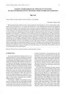
A trend chart for maximum drain current is shown for all NRF1 lots in Fig. 1. Each lot contains 4-7 wafers, thus giving the 300+ total wafers. The lots highlighted in blue signify those used for reliability and qualification activity and were sampled randomly across process. 1050 1000
Imax (mA/mm)
INTRODUCTION Power transistors based on AlGaN/GaN have emerged as an attractive technology for high-power amplification in both commercial and defense applications [1, 2]. Until recently, marketplace acceptance of this new technology was limited in part by lack of a comprehensive reliabilty data set, and the perception of relatively immature manufacturing capabilites. In this paper we describe our first production-ready process, NRF1, and provide details of the qualification methodology followed. Specifically, reliability results are presented that include three-temperature life testing, DC-HTOL, RF-HTOL, ESD, VSWR robustness, autoclave, and temperature cycling. Details of product development are also given that demonstrate the high-performance and across-process repeatability obtained.
Table 1: NRF1 Specification Limits for inline testing. Parameter
950 900 850 800 750 700 650
05287 05304 05311 05324 05330 05339 05349 05365 05371 05375 05384 05404 05406 05411 05426 05431 05434 05435 05436 05440 05441 05444 05447 05450 05460 05462 06001 06039 06041 06043 06055 06056 06059 06060 06062 06073 06081 06092 06097 06105 06108 06115 06117 06119 06120 06122 06124 06126 06146 06150 06164 06165 06167 06170 06182 06189 06208 06212 06213 06225 06226 06228 06229 06238 06239 06285 06287 06291 06293 06295 06297 06310 06311 06313 06315 06316 06318 06319 06320
Abstract In this paper, the qualification of a production GaN process platform is discussed. Details of the process repeatability, reliability and qualification methodologies are covered in detail. Additionally, concurrent product development efforts are also described. Reliability results include three-temperature DC testing that resulted in an activation energy of 2.0eV and DCHTOL testing demonstrating 20-yr drift rates of less than 3% when operated at 150°C.
LOT_NUM
Figure 1: Trend Chart for Imax across process lot. Each lot represents 4-7 wafers.
PRODUCT DEVELOPMENT After process consistency was established, the NRF1 platform was used to launch five commercial products. Three designed for the emerging WiMax market (NPT35015, NPT35050, and NPT25015) and two designed to provide broadband power for a number of general uses (NPTB00025 and NPTB00050). The first product released was the NPT35050 device in September of 2006. The NPT35050 consists of a transistor die attached into a high thermal conductivity CPC single-ended, ceramic package using a AuSi eutectic process. During product development devices were built from numerous NRF1 wafers, highlighted in Fig. 1. This was done to ensure that both the internal matching network and 50-ohm application board gave consistent performance across process. Typically, these devices produce 60-70W of saturated CW power at an operating voltage of 28V and frequency of 3.5GHz, demonstrated in Fig. 2.
CS MANTECH Conference, May 14-17, 2007, Austin, Texas, USA
83
50
proprietary version of the Curtice model and publicly available version of the Angelov model [5].
Gain (dB), Drain Eff. (%)
45 40 Gain (dB) DE (%)
35 30 25 20 15 10 5 0 28
32
36
40
44
48
Pout (dBm)
Figure 2: CW performance of NPT35050 Device.
20
5
16
4
12
3
8
4
2
DE Gain EVM
3300
3400
3500
3600
EVM (%)
Gain (dB), Drain Efficiency (%)
The WiMax performance of the NPT35050 is measured under an OFDM modulated signal. The part delivers 2.5% EVM, 18% efficiency, and 11dB Gain at an output power of 6W and over the large operating bandwidth of 3.3 to 3.8GHz as shown in Fig. 3.
3700
3800
1
Pout (dBm)
Figure 3: OFDM performance as a function of frequency,
After collecting the performance characteristics from multiple devices across several process lots, a final production test plan was released with final specification limits derived from the across-process variation. Numerous devices have been manufactured and tested to this plan and a distribution for Gain at 3.6GHz for over 1,500 devices from multiple process lots is shown in Fig. 4.
9
10
11
12
13
14
Gain @ Pout = 38dBm Figure 4: Distribution of Gain at 3.6GHz and Pout=6W for over 1,500 NPT35050 devices.
The final piece to the product development was developing circuit models for the NRF1 devices. So far compact models have been developed using both a
84
RELIABILITY TESTING Following process and product development, an extensive reliability evaluation was performed. The reliability evaluation was divided into three phases; intrinsic technology tests, product device tests, and product assembly tests. Intrinsic testing focused on validating the basic NRF1 GaN technology by performing fundamental tests such as threetemperature DC lifetests. The product device tests focused on electrical testing specific to the product and included DCHTOL, ESD, thermal imaging, etc. Finally the product assembly level tests focused on packaging aspects such as autoclave, temperature cycling and thermal shock. The NPT35050 served as the technology qualification vehicle for the NRF1 process and was used in all tests listed above. Devices from a minimum of three process lots were used in all reliability testing. Prior to any life testing, the thermal performance of the device was characterized to ensure proper junction temperature calculations. Thermal impedance was measured using a QFI Infrascope II infrared thermal imaging microscope. The measurement was made with a heat sink temperature of 80°C and a thermocouple mounted below the package to measure the case temperature. The bias condition was VDS=28V and IDS=975mA for each device, which is equal to the power dissipated under the RF operating point of Pout=6W and Efficiency = 18%. A total of 8 samples were measured from 3 wafers. Table 2 summaries the results on the 8 devices and demonstrates a consistent thermal performance across process. Table 2: Summary of Thermal Resistance measurements. DUT 1 2 3 4 5 6 7 8
Tcase (°C) 88.50 89.80 88.90 88.10 88.60 88.00 88.20 88.20
AVG STD DEV
88.54 0.59
Tjunction (°C) RTH (°C/W) Pass/Fail 142.00 1.95 PASS 143.00 1.95 PASS 137.00 1.76 PASS 134.00 1.68 PASS 141.00 1.92 PASS 137.00 1.79 PASS 136.00 1.75 PASS 141.00 1.93 PASS 138.88 3.27
1.84 0.11
Three-temperature DC testing was carried out in order to determine the activation energy for the NRF1 process. Testing consisted of DC stress at VDS=28V and IDS=2.34A with ambient temperature adjusted to achieve junction temperatures of 260°C, 285°, and 310°C. For each stress temperature 25-30 devices were tested with stress time ranging from 400 to 1000 hours. A failure criteria of 15% drift of in-situ drain current was used. Failures followed a lognormal distribution and cumulative failure plots were used to assess the MTTF for each temperature group, as shown in Fig. 5.
CS MANTECH Conference, May 14-17, 2007, Austin, Texas, USA
In Fig. 6, the MTTF for each temperature is plotted on an Arrhenius plot and reveals an activation energy of 2.0eV for the NRF1 process platform. When this curve is extrapolated to a typical use temperature of 150°C, a MTTF greater than 107 hours is predicted. 99.00
24
Imax (A)
23 22 21 20 19 18 17
99
16 T-36
T-168
T500
T1000
T1500
T2000
INTERVAL
50.00
10.00
Figure 7: DC-HTOL results for maximum drain current versus test interval out to 2000 hours.
310°C
50
10
285°C 260°C
5.00
1.00
Imax Percent Change (%)
C u m u la tiv e % F a il
Cumulative Fail (%)
T-0
1
1
100
10
1.00
10.00
5000
1000
100.00
1000.00
Time (hr)
Time (hr)
5000.00
Figure 5: Cumulative failure plots with 90% confidence intervals. 8
10
Operating at 150C 7 leads to MTTF>10
7
10
MTTF (hours)
10
-3 -4
20-year Drift
-5 -6 -7 -8 -9 -10 0 10
0
150 C Prediction 0 150 C Extrapolation 0 200 C Data 0 200 C Extrapolation 1
10
2
10
3
10
4
10
5
10
6
10
Figure 8: DC-HTOL results measured at 200°C (red) and converted to 150°C (blue) showing drift out to 20-years.
5
10
4
10
260C
3
10
Ea = 2.0eV
285C
2
10
310C
10
0
10
-2
Time (hr)
6
1
0 -1
1.6
1.8
2.0
2.2
2.4
RF-HTOL testing was carried out in order to verify that the RF stimulus did not induce additional failure mechanisms. A total of 6 samples were stressed at VDS=28V, Freq=2.14GHz, and RF input power sufficient to drive the device into 3dB gain compression (Pout~50W) with the baseplate adjusted to produce a TJ=200°C. Fig. 9 shows the drift in the in-situ Pout versus time for the 6 samples.
Temperature (1000/K) Figure 6: Arrhenius Plot showing activation energy of 2.0eV and MTTF > 107 hours at 150°C.
DC-HTOL testing was carried out at VDS=28V and TJ=200°C for 2000 hours. A 45 piece sample was placed under DC-HTOL stress, with results shown in Fig. 7 for maximum drain current (Imax). The box plots show consistent performance between the 45 samples and minimal drift with time. Figure 8 is used to predict the long term drift rate. In this figure each of the red dots represents the median for the 45 samples at the test downpoints of 0, 36, 168, 500, 1000, 1500, and 2000 hours. The data is fit to a logarithmic relationship versus time and extrapolated forward to 20-years of operation showing a drift of