Gregory Gol'tsman, Boris Voronov, Roman Sobolewski, William E. Keicher, Karl ... Relaxation Time in Nb Persistent Current Qubits,â Yang Yu, William D. Oliver,.
Chapter 21. Quantum Nanostructures and Nanofabrication
Quantum Nanostructures and Nanofabrication RLE Groups Quantum Nanostructures and Nanofabrication Group, NanoStructures Laboratory Academic and Research Staff Professor Karl K. Berggren Postdoctoral Students Kristine Rosfjord Graduate Students Vikas Anant, Bryan Cord, Eric Dauler, Joshua Leu, Delano Sanchez, Joel Yang Visiting Students Stefan Harrer, Daniele Masciarelli, Giovanni Salvatore Technical and Support Staff James Daley, Tiffany Kuhn, Mark Mondol The Quantum Nanostructures and Nanofabrication Group researches the application and fabrication of devices using the foundations of quantum mechanics. We focus on: (1) superconductive devices and materials applied single-photon detection and quantum computing; and (2) nanofabrication methods. Superconductive devices are among the most readily engineered examples of devices exhibiting quantum-mechanical effects. We therefore work with superconductive materials, including efforts in materials, processing, and analysis. Also, because quantum-mechanical effects are primarily observable at microscopic length scale, we develop and implement novel methods of nanofabrication. We take a multi-disciplinary approach to these topics, using techniques from physics, electrical-engineering, computer science, chemistry, and materials science.
21-1
Chapter 21. Quantum Nanostructures and Nanofabrication
Modelling the Optical Properties of Superconducting Nanowire Single-photon Detectors Sponsors: United States Air Force Project Staff: V. Anant, A.J. Kerman, J.K. Yang, E.A. Dauler, K.M. Rosfjord, K.K. Berggren Polarization-sensitive single-photon detectors can be useful for high-speed optical and quantum communication where one can encode information in the polarization of the photon. We have observed that superconducting nanowire single-photon detectors (SNSPD) fabricated at MIT exhibit sensitivity to polarization. For this project, we will investigate the polarization sensitivity for devices with various geometries and conduct numerical simulations that explain the sensitivity. Our SNSPDs consist of a nanowire in a meandering pattern that acts as an optical wire-grid polarizer. In order to corroborate our model with experimental results, we approximated the meander geometry with wire arrays characterized by two parameters: pitch (periodicity) and fillfactor (the ratio of wire-width to pitch). We conducted finite-element-method (FEM) simulations of the absorptance of polarized radiation to wire grids. The simulations show that meanders with small pitch and small fill-factors will exhibit larger sensitivity to photon polarization than meanders with large pitch and fill-factors. We intend to use our results to design SNSPDs that are optimized for enhanced sensitivity to polarization. The FEM simulations also show this sensitivity of SNSPDs with integrated optical cavities that have been reported to exhibit detection efficiencies of 57% at 1550-nm wavelength and 67% at 1064 nm [1].
Aparallel/Aperpendicular
1.5 1.4 1.3 1.2 1.1 1 0.9
200
400 600 cavity thickness [nm]
Figure 1: Plot showing the expected ratio of absoptances for electric fields polarized parallel and perpendicular to the nanowires as a function of cavity thickness for a SNSPD with an integrated optical cavity. The nanowire detector is modelled as an array of 100-nm-wide parallel wires at a 200-nm pitch. The material set and relevant optical constants are given in Ref. [1].
Figure 2: Scanning electron micrograph of a microfabricated structure on a sapphire substrate. The structure is composed of 50-nmwide wires at a pitch of 100 nm. After the underlying NbN is etched, this structure (and others with different fill-factors and wire widths) can be used to measure the dependence of polarization on absorptance.
References:
[1]
K.M. Rosfjord, J.K.W. Yang, E.A. Dauler, A.J. Kerman, V. Anant, B.M. Voronov, G.N. Gol'tsman, and K.K. Berggren, "Nanowire single-photon detector with an integrated optical cavity and anti-reflection coating," in Opt. Express vol. 14, pp. 527-534, 2006.
21-2 RLE Progress Report 148
Chapter 21. Quantum Nanostructures and Nanofabrication
Using Optical Mixtures of Materials to Control Index, Speed of Light, and Transparency Sponsors: United States Air Force Project Staff: V. Anant, A.F. Abouraddy, K.K. Berggren Recent achievements in optical physics have dramatically redefined the limits of attainable optical properties in materials. Novel optical phenomena, including electromagnetically induced transparency [1], slow light [2], and superluminal speed [3] have been demonstrated in diverse physical implementations. Building on our previous work [4], we have developed a unified approach to engineering optical materials that exhibit these phenomena by using mixtures of simple optical materials near resonances. In addition, this approach can be used to realize large and small (much less than 1) indices of refraction and negative permittivity (ε < 0), all while maintaining transparency and without relying on quantum coherence. Previous work in this field has largely been associated with exploiting quantum-optical effects in a single carefully chosen atomic species. In many cases the complexities of this implementation has prevented further application of these effects. Additionally, the strong association with quantum-coherence has suggested that these optical effects are somehow achievable only using multi-level atomic interactions. Finally, the lack of robustness of these methods has meant that, while these effects may be interesting, they are of little practical utility to robust, real-world devices. All of the interesting optical effects mentioned above can be produced using a simple mixture of materials composed of population-inverted and conventional resonances. By using the fact that an incoherent mixture of materials with different optical properties exhibits an optical characteristic that is a superposition of the characteristics of its components, we propose materials that exhibit a number of optical effects (e.g., large refractive index or a large change in index with respect to frequency) without absorption or amplification. Additionally, this approach is independent of the underlying physical origin of the resonances in the system, so may be applied in a variety of atomic, optical, and nonlinear optical systems.
21-3
Chapter 21. Quantum Nanostructures and Nanofabrication
0.5 χ
�
a
χ
0 -0.5 1
χ��
1
c �
a
c
b
d
0 -1
b
d
1
0
χ�� 0
-1
-1
-4
0
4 -4 0 4 detuning, ∆ (a.u.) Figure 1: Plot of real (χ′) and imaginary (χ″) components of susceptibility as a function of detuning frequency, ∆ for active and passive resonances. Plots (a) and (b) are spectra for a passive resonance, while (c) and (d) show an active resonance.
-4
0
4 -4 detuning, ∆ (a.u.)
0
Figure 2: Plot of real (χ′) and imaginary (χ″) components of susceptibility as a function of detuning frequency for mixtures of active and passive resonances shown in Figure 1. Plots (a) and (b) depict a material with an equal mixture of passive and active resonances chosen so that one gets a positive χ′, zero dχ′/dω, accompanied with transparency (χ′′=0). Plots (c) and (d) depict a material where χ′ < 0 and dχ′/dω = 0 at the transparency point. The dashed lines in (b) and (d) show χ′′ for the constituent active and passive resonances.
References: [1]
M. Fleischhauer, A. Imamoglu, and J.P. Marangos, “Electromagnetically induced transparency”, Rev. Mod. Phys., 77, p. 633, 2005.
[2]
L.V. Hau, Z. Dutton, C.H. Behroozi, and S.E. Harris, “Light speed reduction to 17 meters per second in an ultracold atomic gas,” Nature vol. 397, p. 594, 1999.
[3]
L.J. Wang, A. Kuzmich, and A. Dogariu, “Gain-assisted superluminal light propagation” Nature, vol. 406, p. 277, 2000.
[4]
V. Anant, M. Rådmark, A.F. Abouraddy, T.C. Killian, and K.K. Berggren, “Pumped quantum systems: Immersion fluids of the future?”, J. Vac. Sci. Technol. B, vol. 23, p. 2662, 2005.
21-4 RLE Progress Report 148
4
Chapter 21. Quantum Nanostructures and Nanofabrication
Pattern Generation by Using Multi-Step, Room-Temperature, Nano-imprint Lithography Sponsors: AFOSR, Karl Chang Innovation Fund at MIT Project Staff: S. Harrer, J.K.W. Yang, F. Ilievski, K.K. Berggren, C.A. Ross We have demonstrated multi-step, room-temperature, nano-imprint lithography (RTNIL) using polystyrene (PS, average molecular weight 97 kg/mol) as the polymer layer for imprinting complex patterns. Our motivation in pursuing multi-step RTNIL is to create a new patterngeneration method, able to create complex and arbitrary patterns without requiring a custom template for each new pattern. A variety of different forms of NIL have been demonstrated in the past: thermal NIL [1], UV-cured NIL [2], and room-temperature NIL (RTNIL) [3-6]. All of these existing techniques focus on pattern replication using one, or at most two, imprint steps. In our approach, the extent of each of the starting templates is only a fraction of the extent of the desired final pattern; i.e., each template is much smaller than the final pattern. In separate experiments, single, double, and multiple (up to 10) sequential imprint steps were performed at imprint pressures between 3 to 30 MPa. To accomplish this demonstration, we designed and built a tool that controllably and repeatedly translated and pressed a sample into a stationary mold. The demonstrated inter-step alignment accuracy of this tool was ~ 500 nm. To illustrate this capability, we imprinted the letters “MIT” by using ten sequential imprint steps, translating the sample a programmable distance along a single direction in between steps (Figure 1). The molds used in these experiments consisted of rectangular structures of varying aspect ratios, ranging from 150 to 300 nm wide. Before this technique can be used as it is ultimately intended, as a method for the generation of complex patterns across a wide variety of length scales using only a simple set of generic template structures, the imprint polymer distortion and deformation must be minimized and inter-step alignment must be optimized. However, the work suggests that RTNIL may be a useful pattern-generation tool. This development can be thought of as analogousl to the development of the typewriter after the printing press. While a printing press can replicate largescale molds (entire pages of books) at high rates, in the typewriter, the smallest mold unit was a single letter. The typewriter sacrificed throughput in return for flexibility and low cost. Similarly, by removing the difficult and slow step of custom-template manufacturing from the process, our work represents a shift in the way some nano-imprint work might be performed in the future.
21-5
Chapter 21. Quantum Nanostructures and Nanofabrication
300 nm 1
2
5 3
4
5 4 (a) 200 nm
(c)
(b) 150 nm
(d)
Figure 1: Results of a 10-step RTNIL imprint cycle for different mold dimensions: (a) graphical representation of desired final pattern to be printed out. The numbers indicate the order in which parts of the final pattern are imprinted. After the 5th imprint step, the pattern is complete; steps 6-10 create further identical patterns, yielding a total number of 6 completed patterns after the 10th imprint step. We performed several 10-step RTNIL cycles using molds with different feature sizes: The linewidth of the imprinted pattern in (b) is 300nm, the linewidth in (c) is 200 nm, and (d) shows an imprint result for a pattern composing a linewidth of 150 nm. The observed vertical and horizontal misalignment was ~ 500 nm.
References: [1] S.Y. Chou, P.R. Krauss, and P.J. Renstrom, “Imprint lithography with 25-nanometer resolution,” Science, vol. 272, no. 5258, pp. 85-87, 1996. [2]
M. Colburn, S. Johnson, M. Stewart, S. Damle, T. Bailey, B. Choi, M. Wedlake, T. Michaelson, S.V. Sreenivasan, J. Ekerdt, and C.G. Willson, “Step-and-flash imprint lithography: a new approach to high-resolution patterning,” SPIE Conf. on Emerging Lithographic Technologies III, vol. 3676, pp. 379-389, 1999.
[3]
D.-Y. Khang, H. Yoon, and H.H. Lee, “Room-temperature imprint lithography,” Adv. Mater., vol. 13, no. 10, pp. 749-752, 2001.
[4]
D. Pisignano, L. Persano, P. Visconti, R. Cingolani, G. Gigli, G. Barbarella, and L. Favaretto, “Oligomer-based organic distributed feedback lasers by room-temperature nanoimprint lithography,” Appl. Phys. Lett., vol. 83, no. 13, pp. 2545-2547, 2003.
[5]
E. Mele, D. Pisignano, M. Mazzeo, L. Persano, and G. Gigli, “Room-temperature nanoimprinting on metallo-organic complexes,” J. Vac.Sci. Technol. B,vol. 22, no. 3, pp. 981-984, 2004.
21-6 RLE Progress Report 148
Chapter 21. Quantum Nanostructures and Nanofabrication
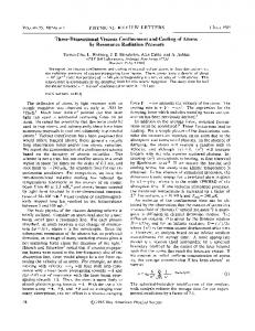
Increasing Detection Efficiency of Superconducting Nanowire Single-photon Detectors Sponsors: United States Air Force Project Staff: K.M. Rosfjord, J.K.W. Yang, E.A. Dauler, A.J. Kerman, V. Anant, K.K. Berggren Superconducting NbN-nanowire single-photon detectors (SNSPDs) [1] are an enabling technology for high-performance single-photon optical systems. Examples of these systems include ultra-long range communications [2], integrated circuit testing [3] and quantum cryptography [4]. These systems require the detectors to have high detection efficiency and photon-counting rates, and low dark-count rates and jitter. This work has aimed to increase the detection efficiency of SNSPDs. The SNSPDs are limited in their efficiency of detection due to transmission through and reflection from the device. To combat these losses we integrated optical enhancements in the form of an anti-reflection coating and optical cavity. These enhancements enabled us to achieve a detection efficiency of 57% at 1550-nm wavelength [5]. This detection efficiency contrasts with previously reported detection efficiencies of 17% at 1550-nm wavelength [6]. A schematic cross-section and transmission electron micrograph of the detector integrated with an optical cavity are shown in figure 1.
Figure 1(a) Schematic cross-section of photodetector (not to scale) integrated with an optical cavity and anti-reflection coating to reduce loss of photons from reflection and transmission. (b) Transmission electron micrograph of cross-section of fabricated device with optical cavity. The cavity shown here was fabricated for calibration purposes and was thicker than those used to increase the detection efficiency.
The SNSPDs are also limited in their efficiency of detection by the dimensions of the nanowire they employ. We are currently developing a process, utilizing slant evaporation, which will enable us to lower the width of the nanowire and increase the fill factor of the meander. By changing these physical properties of the meander and coupling this process with our now established optical enhancements, we aim to again increase the detection efficiency of these devices. References: [1] G.N. Gol'tsman, O. Okunev, G. Chulkova, A. Lipatov, A. Semenov, K. Smirnov, B. Voronov, A. Dzardanov, C. Williams, and R. Sobolewski, “Picosecond superconducting single-photon optical detector,” App Phys Lett, vol. 79, no. 6, pp. 705-707, Aug. 2001.
21-7
Chapter 21. Quantum Nanostructures and Nanofabrication
Robust Shadow-mask Evaporation via Lithography-controlled Undercut Sponsors: QuaCGR Fellowship, AFOSR Project Staff: B. Cord, C. Dames, J. Aumentado (National Institute of Standards Technology), K.K. Berggren Suspended shadow-mask evaporation is a simple, robust technique for fabricating Josephson junctions using electron-beam lithography. The basic process entails the fabrication of an undercut structure in a resist bilayer to form a suspended “bridge,” followed by two angleevaporations of superconducting material with a brief oxidation step in between, resulting in two overlapping wires separated by a thin oxide layer. Josephson junctions with sub-20-nm diameters are of particular interest in a variety of superconductive devices, including quantum bits. Unfortunately, standard shadow-mask fabrication techniques are unreliable at linewidths below 100 nm, requiring the development of a novel process for the fabrication of nanoscale Josephson junctions. While most previous processes used PMMA for the top (imaging) layer and a PMMA/MAA copolymer for the bottom (support) layer, our process uses a PMMA/PMGI bilayer. This resist system allows the two layers to be developed separately, ensuring that the imaging layer is not biased during development of the undercut and allowing the process to achieve the full resolution of the PMMA layer (fig. 2). Additionally, the extent of the undercut in the support layer can be precisely controlled by defining it lithographically, making it possible to repeatably fabricate undercut regions as large as 600 nm. Extensive modeling of both the exposure and development processes was used to verify our results. Using Monte Carlo and mass transfer simulations, we were able to produce a model that closely matches experimental data. With the process fully characterized, it is possible to produce a wide range of linewidth/undercut combinations. This robustness, combined with the high resolution of PMMA, will allow the reliable fabrication of sub-20-nm Josephson junctions. development rate (nm/sec)
5 4.5
75% CD-26
4 3.5 3
60% CD-26 PMMA
2.5 2 1.5 1 0.5 0 1
Figure 1: Scanning electron micrograph of a 16-nmwide, 10-nm-thick evaporated titanium-gold line fabricated using the PMMA/PMGI process.
21-8 RLE Progress Report 148
10 100 dose (µC/cm2)
1000
Figure 2: Contrast curve plots for PMGI using two different dilutions of CD-26 developer. Contrast data for PMMA developed in a 3:1 IPA:MIBK solution is shown for reference.
Chapter 21. Quantum Nanostructures and Nanofabrication
Enhancing Etch Resistance of Nanostructured Spin-on-Glass Electron Resist via Post-Develop Electron Bombardment Sponsors: Lincoln Laboratory Project Staff: J.K. Yang, V. Anant, K.K. Berggren Hydrogen silsesquioxane (HSQ) has been used recently as a high-resolution, negative-tone, electron-beam resist[1]. Although HSQ is a good etch mask in chlorine reactive-ion etching (RIE), its poor etch resistance in fluorine RIE makes it undesirable as a mask for etching materials that etch only in fluorine. In this work, we increased the etch-resistance of hydrogen silsesquioxane (HSQ) in CF4 chemistry via electron-beam curing at high doses. We observed a decrease in the HSQ etch rate by as much as 40% after resist exposure to electron doses of 85 mC/cm2 (Figure 1). This property of the resist was exploited to fabricate 15-nm-wide superconducting NbN nanowires. We achieved this by subjecting HSQ to an exposure-develop-exposure step prior to pattern transfer into NbN. The first electron beam exposure defined the nanowires at doses of ~400 µC/cm2. This was followed by resist develop in Shipley Microposit MF CD-26, resulting in 15-nm-wide HSQ structures. The nanostructures were then re-exposed at 50 mC/cm2 before RIE to toughen the resist, which would otherwise not survive the etch. Electron exposures were performed at 30 kV acceleration voltage using a Raith 150 electron-beam lithography tool. We demonstrated that the second electron exposure does not decrease the resolution of the nanostructures by comparing images of 15-nm-diameter HSQ nano-pillars before and after reexposure (Figure 2). This process will enable nanofabrication with thinner resist, therefore avoiding problems such as resist collapse and reduced resolution that are associated with thicker resist layers.
Etch rate (nm/min)
24
20
15
16
12 0.1
1
10
2
100
1000
Dose (mC/cm ) 15 Figure 1: Plot of HSQ-etch rate with respect to electron exposure dose. We successfully decreased the etch rate of HSQ by exposing the resist to high doses of electrons. Reactive-ion etch (RIE) conditions were 100-W rf power, 15-V DC self-bias potential, and 15[-?]mT with 15 sccm CF4.
Figure 2: Scanning electron micrograph (SEM) images of HSQ nano-pillars arranged in a hexagonal close-packed structure on Si substrate before (a) and after (b) curing with 50-mC/cm2 electron dose. There was no observable degradation in the resist shape or dimension due to the second exposure at these dimensions.
References: [1] H. Namatsu, Y. Takahashi, K. Yamazaki, T. Yamaguchi, M. Nagase, and K. Kurihara, "Three-dimensional siloxane resist for the formation of nanopatterns with minimum linewidth fluctuations," Journal of Vacuum Science & Technology B, vol. 16, pp. 69-76, 1998.
21-9
Chapter 21. Quantum Nanostructures and Nanofabrication
Modeling of Electrical and Thermal Response of Superconducting Nanowire Single Photon Detectors (SNSPD) Sponsors: Lincoln Laboratory Project Staff: J.K. Yang, K.K. Berggren The response time of superconducting nanowire, single-photon detectors (SNSPD) is in the order of several nanoseconds [1, 2]. This detector works by the formation of a photon-induced resistive barrier across a superconducting nanowire that is biased close to its critical current. Detected photons result in measurable voltage pulses with very fast rise times and a slower decay. We modeled the full electrical and thermal response of a NbN SNSPD to the absorption of a single photon. The thermal response was modeled by a one-dimensional, time-dependent heat equation incorporating power dissipated by Joule heating in the resistive segment of the wire and heat conduction along the wire and into a sapphire substrate. The electrical model consists of the SNSPD, modeled as an inductor in series with a time-varying resistor shunted by a 50-ohm transmission line and a current bias. This model predicts the growth of the normal region leading to the increase in the total electrical resistance with time as more of the wire heats up and switches into the normal state. However, the resistance does not build up indefinitely since the current flowing through the wire drops as it is diverted into the transmission line once resistance develops in the wire. The model will also enable us to predict performances of devices made of different materials. 8 200 nH 400 nH
time
resistanceResistance across wire (kΩ) across wire/k Ω
7 6 5 4 3 2 1 0
0
50
100
150
200
250 time/ps
x (nm)
Figure 1: Plot of simulation data showing the temperature evolution in a short segment (1.5 µm) of a longer nanowire (with a total kinetic inductance of 200 nH) after a photon-induced resistive barrier forms across the nanowire at t = 0, x = 750 nm. Temperature information is depicted in the color with a corresponding color-map shown on the right in units of Kelvin. The temperature increases quickly and reaches a maximum at about ~50 ps after photon absorption.
21-10 RLE Progress Report 148
300
350
400
450
500
ti me (ps)
Figure 2: Plot of simulation data showing the total resistance built up across a superconducting nanowire after the formation of a resistive barrier for wires of different total kinetic inductances.
Chapter 21. Quantum Nanostructures and Nanofabrication References: [1] A.J. Kerman, E.A. Dauler, W.E. Keicher, J.K.W. Yang, K.K. Berggren, G. Gol'tsman, and B. Voronov, "Kinetic-inductance-limited reset time of superconducting nanowire photon counters," App. Physics Lett., vol. 88, pp. -, 2006. [find page numbers!] [2]
K.M. Rosfjord, J.K.W. Yang, E.A. Dauler, A.J. Kerman, V. Anant, B.M. Voronov, G.N. Gol'tsman, and K.K. Berggren, "Nanowire Single-photon detector with an integrated optical cavity and anti- reflection coating," Optics Express, vol. 14, pp. 527-534, 2006.
Publications Journal Articles, Published 1. “Pumped quantum systems: immersion fluids of the future”, Vikas Anant, Magnus Radmark, Ayman F. Abouraddy, Thomas C. Killian, and Karl K. Berggren, J. Vac. Tech. B, 23(6), 2662-2667, (2005). 2. "Fabrication Development for Nanowire GHz-Counting-Rate Single-Photon Detectors," Joel K. W. Yang, Eric Dauler, Antonin Ferri, Aaron Pearlman, Aleksandr Verevkin, Gregory Gol’tsman, Boris Voronov, Roman Sobolewski, William E. Keicher, Karl K. Berggren, IEEE Trans. Appl. Supercond., 15, 626-630, (2005). 3. “Energy Relaxation Time in Nb Persistent Current Qubits,” Yang Yu, William D. Oliver, Janice C. Lee, Karl K. Berggren, and T. P. Orlando, IEEE Trans. Appl. Supercond., 15, 845-848 (2005). 4. “Resonant Readout of a Persistent Current Qubit,” Janice C. Lee, William D. Oliver, Terry P. Orlando, and Karl K. Berggren, IEEE Transactions on Applied Superconductivity,15,841-844, (2005). 5. “Mach-Zehnder Interferometry in a Strongly Driven Superconducting Qubit,” William D. Oliver, Yang Yu, Janice C. Lee, Karl K. Berggren, Leonid S. Levitov, and Terry P. Orlando, Science, 310, 1653-1657, (2005). 6. “Nanowire Single-Photon Detector with an Integrated Optical Cavity and Anti- Reflection Coating,” Kristine M. Rosfjord, Joel K. W. Yang, Eric A. Dauler, Andrew J. Kerman, Vikas Anant, Boris M. Voronov, Gregory N. Gol’tsman, and Karl K. Berggren, Optics Express, 14(2), 527-534, (2006). 7. “Kinetic-inductance-limited reset time of superconducting nanowire photon counters,” Andrew J. Kerman, Eric A. Dauler, William E. Keicher, Joel K. W. Yang, Karl K. Berggren, Gregory N. Gol’tsman, and Boris M. Voronov, Applied Physics Letters, 88, 11111611111163, (2006). 8. “781-Mbit/s photon-counting optical communications using a superconducting Nanowire detector,” Bryan Robinson,Andrew Kerman, Eric Dauler, Richard Barron, David Caplan, Mark Stevens, John Carney, Scott Hamilton, Joel Yang and Karl Berggren, Optics Letters, 31(4), 444-446 (2006).
21-11