RAM Design Using Quantum-Dot Cellular Automata K. Walus, A. Vetteth, G. A. Jullien, V.S. Dimitrov ATIPS Laboratory, University of Calgary Calgary, Alberta, Canada, T2N 1N4 (403) 210-5433
[email protected],
[email protected],
[email protected],
[email protected] ABSTRACT Quantum-dot cellular automata (QCA) is a novel and potentially attractive technology for implementing computing architectures at the nano-scale. By applying a set of simple layout rules, arbitrary circuits can be made using QCA cells. In this work, we describe the design and layout of a QCA random access memory (RAM), showing the layout of individual memory cells, as well as, a suggested layout for a 1x4 RAM. The RAM is based on a 2D grid of row addressable memory cells. Each of the memory cells in the RAM uses 158 QCA cells. Assuming that we can fabricate cells which are separated by 10nm, memory capacities of over 1.6 Gbit/cm2 can be achieved. Simulations on the proposed memories were carried out using QCADesigner, a layout and simulation tool for QCA, by iteratively applying an intercellular Hartree-Fock approximation. Keywords: Quantum cellular automata, random access memory, computational nanotechnology, QCA layout, digital design.
1
INTRODUCTION
QCA has gained significant popularity in recent years. This is mainly due to rising interest in creating computing devices at the nano-scale. At such scales, QCA has an inherent advantage over conventional integrated circuit technologies (such as CMOS) in that its performance increases as feature sizes are reduced, whereas CMOS exhibits decreasing performance with decreasing feature sizes. At this time, it is unclear whether or not this technology will replace such a firmly embedded technology as CMOS, but investigations into modeling and design have demonstrated that QCA has many powerful features some of which are not available in CMOS [1][7]. Although many fabrication challenges have still to be overcome [6][7], the simple design nature of QCA makes it attractive for investigation of new circuit topologies [10]. QCA topologies are not simple translations of standard circuit layouts; new ideas for translating standard logic units into QCA are needed. One of the interesting features of QCA is that there is no fixed connection strategy, and hence, it should be possible to apply optimization algorithms such as
genetic algorithms to minimize the number of cells in a design. This work is focused on the design and layout of a simple RAM architecture. We aim to maximize the memory density and focus on a layout that is minimal in its use of cells. Other design strategies have been proposed such as the SQUARES formalism [2], which is based on a set of reusable function blocks. Although this strategy simplifies the layout of circuits, it is not optimal in its use of cells and hence, produces large designs.
2
QCA RANDOM ACCESS MEMORY (RAM)
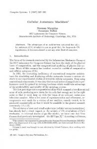
Unlike CMOS memory, QCA has no equivalent for “static memory”. Memory storage is based on a circulating memory model similar to that proposed by the H-Memory architecture [3], which is a QCA implementation of a binary tree. The memory loop is divided into four consecutive clocking zones, each latching in succession. The stored memory continuously circulates in the loop until a write operation is performed at which time the memory is changed. Any read operation does not alter the memory. Although serial structures such as the proposed HMemory consume less clocking zones per bit, a parallel memory is more compatible with conventional architectures. Hence, this paper presents a layout of a conventional parallel memory architecture using QCA. The architecture is based on a simple 2D grid layout of memory cells. The rows of memory cells are addressed using a QCA decoder. The system diagram for the RAM is shown in Figure 1.
MC
MC
MC
MC
MC
MC
MC
MC
MC
MC
MC
MC
MC
MC
MC
MC
I/O 0
I/O 1
I/O 2
I/O 0
A0
2-to-4 Decoder A1
R/W
Figure 1 System diagram of QCA RAM layout.
Each of the rows of memory cells is addressable with the decoder. Once addressed, each memory cell in the RAM will be either written to or read from depending on which action is selected. The word size of the RAM is determined by the number of memory cells in each of the rows and can be increased by simply adding memory cells. To increase the total capacity of the RAM, the address space must also be increased. To do this we need to scale up the decoder, as well as, add rows of memory cells to the array.
2.1
QCA MEMORY CELL
The proposed QCA memory cell is made of QCA logic gates, i.e. AND, OR and NOT gates. Moreover logic functions unique to the QCA technology such as the coplanar wire crossing, inversion chain [1] have been extensively exploited to ensure optimal design. Each memory cell consists of 158 QCA cells. Since the design consists of a simple 2-dimensional grid structure, an n-bit memory would have O(n) cells. If we assume that cells are spaced 10nm apart, the design has a storage capacity of over 1.6 Gbit/cm2. Further optimization could significantly increase this figure, possibly by an order of magnitude. One such optimization would be to store two or more bits per loop and maintain a parallel architecture. The circuit schematic for the proposed QCA memory cell is shown in Figure 2.
Figure 2 QCA memory cell circuit schematic. The memory value is constantly circulated inside the memory loop until the Write/Read and Row Select wires are polarized to 1, at which time the incoming input is fed into the memory loop and circulated. If the Row Select is polarized to 1 and the Write/Read is polarized to 0, the current memory value inside the loop is fed to the output. The circuit schematic shown is laid out to match that of the actual QCA layout. The final memory cell layout is shown in Figure 3.
Figure 3 QCA memory cell layout. The memory loop in the center of the cell is clearly distinguished. Each shade of gray represents a different clocking zone. It was shown in previous work [3][5] that 4 clocking zones, each delayed by π 4 radians, are sufficient to effectively control the flow of information in any QCA circuit. The darkest shaded cells are attached to clock 0, and the others are represented by successively lighter shades. The cells which have polarizations, shown directly above them, are fixed to that polarization. Fixed polarization cells are required since the fundamental logic gate in QCA is the majority gate, by fixing one of its inputs to either a 1 or 0 we can generate the standard AND, OR operations [1]. The control signals arrive at the memory cell from the right and the output signals propagate to the left. This memory cell is laid out such that it could easily be placed inside an array of other memory cells forming the complete RAM. The overall use of cells in this unit could have been reduced by placing some of the interconnects closer together. Although this would reduce cell use, problems could arise from cross-talk between cell interconnects. In this design, we have used a separation of at least two cells between signal interconnect wherever the possibility for cross-talk exists; an example is the gap between the memory loop and some of the fixed polarization cells. There are some areas in the design where this was not necessary; e.g., interconnect attached to clocks 0 and clock 2. In this case, there is no problem with cross-talk because the two interconnects do not simultaneously transmit.
2.2
Decoder
In order to address any row of the QCA memory, we need a decoder circuit which generates a Row Select signal to the appropriate row in the memory based on an address applied at the input. Figure 4 shows the layout of the QCA decoder.
Figure 4 QCA decoder.
Extending this design to larger word sizes involves adding memory cells to each row. Increasing the number of addressable words requires scaling the decoder and adding more rows of memory cells. One of the challenges to using this design for larger memory sizes is that the delay is directly proportional to the row length since the Row Select signal has to propagate proportionately further to the outside memory cells.
3 The two control lines S0 and S1 run as inversion chains. These signals are tapped off at appropriate locations so as to obtain the required logic for a0, a1, a2 and a3. For example, a3=S0S1. As an example of the operation of this circuit, if both S0 and S1 are polarized to 1, then a3 is active and polarized to 1 and a0, a1, and a2, polarize to 0. This decoder is easily scalable to larger address sizes. We believe, however, that there are some fundamental limits to the scaling of this design. This is a result of the tolerance of coplanar interconnect crossings, heavily employed in this design, to asymmetries in the cells due to fabrication errors. We discuss this briefly in the section on fault tolerance.
2.3
1x4 QCA RAM
Using the memory cell described earlier and the QCA decoder, we can create a 2D addressable array. In Figure 5, we show a 1x4 QCA RAM. The output from each of the cells is propagated downward through a serial OR array. The use of a serial OR array is necessary at this time since the equivalent of a tri-state buffer is not available in QCA technology.
SIMULATION
Simulations were carried out using QCADesigner [4] where an adiabatic intercellular Hartree-Fock approximation is implemented [8]. This approximation assumes that the cells are only coupled through expectation values of polarization. The stationary state of each of the cells is computed using the following:
Eik, j Pi =
2γ
∑P
Eik, j 1 + 2γ
j
∑ Pj
2
Where Pi is the polarization state of the cell, and Pj is k
the polarization state of the neighboring cells. Ei , j is the kink energy between cells i, and j and represents the energy cost of oppositely polarized cells. γ is the tunneling potential and is used to clock the circuit as described in [4]. The simulation iteratively computes the state of each cell until the system has converged. Once the circuit has converged, the output is recorded and new input values are set.
3.1
PERFORMACE
At this time, it is difficult to estimate the speed performance of such a design as a final physical implementation of QCA has still to be established. Proposed molecular implementations have been reported to achieve speeds of excess of 1THz. One possible measure of performance is the number of clock cycles that are required between writing a bit of data to the memory cell and reading that same bit at the output. We can extract this from the clocking of the memory cell. We can see from the memory cell layout that it takes one complete clocking cycle for information to propagate from the input to the memory loop. As well, it takes another clock cycle for the information to exit the memory loop. This means that 2 complete clocking cycles are needed to completely pass information through the memory. Figure 5 1x4 RAM layout.
For a complete RAM, this figure would increase since external logic, such as the decoder, would require additional clocking cycles to operate. The total delay of any QCA circuit is directly proportional to the number of clocking zones that are along the longest information path. This presents other challenges since signals arrive at completely different times at the output. One solution is to add redundant clocking zones to shorter paths in the circuit. This could be done in such a way so that the information arrives at the output simultaneously.
3.2
FAULT TOLERANCE
It has been shown that asymmetries (translations) in the position and size of the dots within the cell result in cellcell response functions, which are moved to either of the two possible polarizations [9]. If the translation is minor, then the non-linear cell-cell response function can correct for the fault. The tolerance to translation errors depends on the randomness along the interconnect. For example, if the translation of one cell is positive and the translation of the adjacent cell is negative by the same magnitude, then there is a balance and the correct signal is able to propagate. It is believed that fabrication errors will probably arise in bunches; i.e., many cells along an interconnect will exhibit the same fault. In this case, the tolerance for errors becomes even smaller, possibly preventing any design to function properly. Significant changes in the cell-cell response will cause a “lock” effect where one cell remains in a fixed polarization state. A design such as this may not be completely feasible if these asymmetries are large and shifting of the cell-cell response function is significant. This issue would plague virtual every conceivable design. Unfortunately, at this time, it is unclear what the final implementation of QCA will be and what tolerances will be acceptable with that implementation. There is an effort underway to determine if higher level solutions can be found to increase the fault tolerance of QCA circuits, possibly at an algorithmic level.
4
CONCLUSION
In this work, we have proposed a design and layout for a QCA RAM. The design utilizes a circulating memory scheme in which memory is held in a constantly circulating loop. The overall architecture is based on a conventional 2D grid of memory cells which can be addressed by row using a QCA decoder. The layout was simulated by iteratively applying the intercellular Hartree-Fock approximation. Each of the memory cells in the grid consumes 158 QCA cells. Assuming that the cells are separated by 10nm, memory capacities of over 1.6 Gbit/cm2 can be achieved. There are further opportunities for optimization which could lead to storage densities greater than this. Future work will focus on optimizing this layout, as well as, increasing the fault tolerance by reducing the number of coplanar crossovers and possibly fault tolerant algorithms, and architectures. Although it is difficult to
report any speed performance measures, application of this design to molecular QCA implementations could lead to the reported potential THz range.
5
ACKNOWLEDGEMENTS
The authors acknowledge financial support from iCORE, the Natural Sciences and Engineering Research Council of Canada, the Micronet Network of Centres of Excellence, the University of Calgary, and the Canadian Microelectronics Corporation.
REFERENCES [1] Tougaw, P.D., Lent, C.S., “Logical devices implemented using quantum cellular automata”, J. Appl. Phys., 75 (3) 1818, 1994 [2] D. Berzon, T J Fountain, “A Memory Design in QCA’s using the SQUARES Formulism”, Technical Report, University Collage London, UK, 1998 [3] S. Frost, A.F. Rodrigues, A.W. Janiszewski, R.T. Raush, P.M. Kogge, “Memory in Motion: A Study of Storage Structures in QCA”, First Workshop on NonSilicon Computing, 2002 [4] Walus, K. “QCADesigner Homepage”, http://www.atips.ca/projects/qcadesigner, ATIPS Laboratory, University of Calgary, Calgary, AB, 2002 [5]Hennessy, K., Lent, C., “Clocking of molecular quantum-dot cellular automata”, J. Vac. Sci. Technol.,, B 19 (5) 1752, 2001 [6] Islamshah, A., Orlov, A.O., Kummamuru, R.K., Bernstein, G.H., Lent, C.S., Snider, G.L., “Experimental demonstration of a leadless quantum-dot cellular automata cell”, Appl. Phys. Lett., 77 (5) 738, 2000 [7] W. Porod, “Quantum-dot devices and quantum-dot cellular automata”, Inter. J. Bifurcation and Chaos, 7 (10) 2199, 1997 [8] G. Toth, “Correlation and Coherence in QuantumDot Cellular Automata”, Ph.D. Thesis, University of Notre Dame, 2000 [9] M. Governale, M. Maccuci, G. Iannaccone, C. Ungarelli, “Modeling and Manufacturability Assessment of Bistable Quantum-Dot Cells”, J. Appl. Phys., 85 (5) 2962, 1999 [10] A. Vetteth, K. Walus, G. A. Jullien, V. S. Dimitrov, “Quantum Dot Cellular Automata Carry-Look-Ahead Adder and Barrel Shifter”, IEEE Emerging Telecommunications Technologies Conference, 2002