Random Telegraph Signal Noise SPICE Modeling for Circuit Simulators C . Leyris, S. Pilorget, M. Marin, M. Minondo, H. Jaouen STMicroelectronics, FTM Crolles site, 850 rue Jean Monnet, 38926 Crolles Cedex, France
[email protected] Abstract— In small area MOSFET devices widely used in analog and RF circuit design, low frequency noise behavior is increasingly dominated by Random Telegraph Signal noise. For analog circuit designers, awareness of these single electron noise phenomena is crucial. If optimal circuits are to be designed these effects can aid in low noise circuit design if used properly, while they may be detrimental to performance if inadvertently applied. This paper presents the investigation of Random Telegraph Signal (RTS) implementation in circuit simulator. A model based on Shockley-Read-Hall statistics to explain the behavior is presented. This work takes into account the impact of noise power spectral density (PSD) dispersion. The distinctiveness of the noise variations is discussed in detail and the proposed mechanisms behind the phenomena are viewed in light of the collected data. Results are compared with experimental data.
I. INTRODUCTION Constant MOSFET downscaling makes the speed of the devices higher, lowers the power consumption per function and enables an ever-increasing level of integration. Though analog circuits benefit from higher speed, the reduced voltage headroom makes it increasingly difficult to maintain a sufficient signal to noise ratio, making low noise design more and more important. For speed and functional density reasons, it is attractive to use small-area devices. Unfortunately, small devices have worse low frequency noise (LFN) behavior, which means that LFN performance is a dominant issue in ever more circuits [1], [2]. The present trend shows that thermal and 1/f noise are no longer the main contributing noise components. As a matter of fact, the main LFN contributing factor in down scaled MOSFETs is Random Telegraph Signal (RTS) noise [3], [4]. All these noise phenomena, which may show up in circuit measurement, are not currently incorporated in any circuit simulator. There was no good understanding of device noise in these circuits neither convenient techniques were not available to analyze and simulate these noise contributions. As a result, measured LFN performances are not often directly compared to simulations and if comparisons are made at all, correspondence within a few dB is usually considered quite acceptable. Moreover, LFN in small devices shows extreme variability. Measured LFN can vary by
1-4244-1124-6/07/$25.00 ©2007 IEEE.
187
several orders of magnitude between different identical devices [5]. For better circuit design, awareness of the LFN phenomena as RTS noise is crucial. A detailed investigation of the implementation in circuit simulator of RTS noise is carried out in this work. We demonstrate that our model takes into account LFN die-todie dispersion by evaluating the RTS noise dispersion from weak to strong inversion in linear and saturation ranges. Simulations are compared with experimental data. II.
OVERVIEW OF LOW FREQUENCY NOISE MODELS
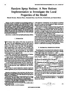
A. Classical approach A current flowing through a solid-state device at fixed biases can be characterized by the occurrence of random fluctuations. The usual associated low frequency noise PSD often shows a 1/f shape, where f is the frequency. In the case of MOSFET, these variations may be associated with carrier number fluctuations (McWhorter model) [6], with mobility fluctuations (Hooge empirical relation) [7], or with carrier number fluctuation inducing mobility fluctuations [8]. The scaling down of device dimensions can drastically change the shape of the fluctuations in the time domain as well as the corresponding noise PSD and is the result of RTS noise contributions [9]. This change in relative current fluctuations and its associated current noise PSD are shown in figure 1. B. Random Telegraph Signal Noise in MOSFET The models presented in the previous section work well for large-area devices. For small devices, they break down because the number of mobile charge carriers is no longer large and behavior of individual charge carriers becomes visible and significant. Theory predicts that as soon as the number of free carriers in the device decrease far enough, it will be possible to observe behavior of individual carriers. This is in line with experimental data, as active device area became smaller and smaller, it becomes possible to observe RTS noise in MOSFET at room temperature. Nowadays, RTS noise is the dominant noise mechanism in small-area devices, typically with active areas of less than 1 µm². Discrete drain current switching (RTS noise) is generally observed at fixed bias values. At least two current levels are
present (fig.1b). RTS is caused by trapping of an individual carrier, due to a single active trap in the oxide, or by a scattering centre in the vicinity of the inversion layer of the device. The associated RTS current noise PSD, SId(f), or socalled Lorentzian spectra, is characterized by a constant plateau (P) at low frequencies and a 1/f² roll-off at higher frequencies (Fig.1a). Its typical expression is: SI D (f ) =
P f 1+ fc
2
=
4 A τ ∆Id2
(1)
1 + (2πf )2 τ 2
Where f is the frequency, fc the corner frequency (fc=1/2πτ), τ the characteristic time constant of the trap (1/τ=1/τe+1/τc) and A the loading factor related to the trap occupation probability. The coefficient A can be written as [10]: τe τc δf = A = f t (1 − f t ) = kT − t 2 δE E = EF ( τe + τc )
(2)
Where ft is the trap occupancy probability function, T is the absolute temperature, k is the Boltzmann constant, and τe, τc the emission and capture times, respectively. 10-19
(a) P 2.5
10-21
t1
2.0
1/f²
1.5
10-22
∆Id/Id (%)
SID (f) (A2/Hz)
10-20
1.0 0.5
∆Id
10-23
-1.0 -1.5 0.000
10-24 100
(b) 0.002
101
t0 0.004
0.006
time (s)
102
0.008
0.010
103
104
∆ Id x g q 1 − t =η m Id Id WLCox t ox
(4)
where gm is the transconductance, η a fit parameter, xt the trap depth with respect to the silicon-oxide interface, tox the oxide thickness, W and L the width and the length of the transistor, respectively. By combining time and frequency domain measurements, the Lorentzian plateau evolution for a single trap can be obtained by: 2
2 f t (1 − f t ) g mq x t (5) 1 − η π fc WLCox t ox From low frequency noise measurements performed on a single transistor and a given voltage bias, we obtain the noise PSD of the signal. The noise PSD can typically be divided into three contributions: 1/f noise, RTS noise and white noise. Using (1) and (2), the noise PSD is calculated as follows: P=
2 2 f t ( m,σ) (1 − f t (m,σ) ) gmq x t 1 η − π fc WLCox t ox (6) α Nt SId (f ) = + ∑ +B 2 f i=1 1 + f fc
0.0 -0.5
RTS parameters show a strong dependency on the operating conditions, i.e. the drain (VDS), gate (VGS) and substrate (VBS) biases and on the temperature T. The trap characteristics directly impact the shape of the noise PSD of the signal. The relative drain current RTS amplitude can then be calculated assuming that the trapping of an elementary charge in the channel changes the local conductivity [11]. It has been shown that the relative drain current RTS amplitude for a single trap can be approximated by [12]:
105
frequency (Hz) Figure 1. R.T.S noise power spectral density (Lorentzian shape) (a) and corresponding relative drain current fluctuations of a small-area MOSFET (b)
A simple two-level RTS could be defined by two parameters in the frequency domain: The corner frequency (fc) and the plateau value (P) (figure.1a). In the time domain, RTS is defined by three parameters: The time spent in the up or high current state (t1), the time spent in the down or low current state (t0) and the amplitude ∆Id. The mean values of t0 and t1 are τ0 and τ1 and they are defined as the up and down time constants. They usually correspond to an empty or occupied trap site, in other words, the average carrier capture or emission times. It has been demonstrated that the up and down times follow an exponential distribution, given by [11]: t 1 p0,1 (t) = exp − (3) τ0,1 τ0,1
188
Where i is the number of RTS contributions induced by i active traps at a same time and B the thermal noise. The parameter α is the flicker noise coefficient. For submicron transistors, the noise power spectral density is dominated by RTS noise. In this case, the value of α is often negligible. B represents the white noise component which corresponds to the thermal noise. III.
IMPLEMENTATION OF RTS NOISE CONTRIBUTION IN CIRCUIT SIMULATORS
Standard compact models such as BSIM3 and BSIM4 [13] or PSP102 [14] classically include flicker noise and thermal noise contributions. Due to the particular nature of RTS noise, no compact modeling is provided so far. Using a VerilogA code adapted in our case to an original BSIM3 model, it has been possible to include RTS equations given in the previous section and simulate this major contribution with this solution in the SPICE simulator ELDO from Mentor Graphics. It has been shown that measured LFN PSD
can vary by several orders of magnitude between different nominally identical devices (Figure 2).
Hz (figure 5). In this case, we characterized no 1/f noise component but a noise PSD dominated by RTS components due to trap competition [15].
1E-16
σ1 σ3
1E-19
1E-22 1E-23
σ2 Trap3
1E-20 1E-21
m2 Trap2
1E-18
SId (f) (A²/Hz)
m3
m1
Max of PSD
1E-17
Trap1
W/L = 0.35/0.28 10 dices IDS = 2 µA VD = 2.7 V Min of PSD VG = 2 V
1E-24 1.E+00
1.E+01
1.E+02
1.E+03
1.E+04
1.E+05
1.E+06
0
10
20
30
40
Frequency (Hz)
Figure 2. Maximal and minimal computed noise PSD with respected to experimental ten devices noise PSD.
For each studied device, the relative drain current fluctuation is still similar whereas the trap occupation probability values (ft) change significantly (Figure 3).
Frequency Histogram
∆Id/Id
W/L = 0.35/0.28 10 dices IDS = 2 µA VD = 2.7 V VG = 2 V
ft
-0.5
0.5
70
80
90
100
All the RTS noise parameters (corner frequencies, Lorentzien’s plateaus) required for our noise computation are extracted from this low frequency noise measurement. By considering complementary noise sources (SPICE_RTS), the simulated PSD behavior changes significantly. The noise power spectral density computed from equation 6 shows a good correlation with experimental PSD. Moreover, the average PSD obtained from ten transistors do not tend towards 1/f noise as often used [16]. The average PSD is fully dominated by RTS noise in submicron transistors. 1E-18
1.5
2.5
∆Id/Id (%)
Figure 3. Relative drain current fluctuations evolution for ten identical structures (time domain)
Moreover, following the McWhorter approach, the corner frequency associated to an active trap remains constant. Based on equation 6 the variation of ft explains the variability of the measured PSD. Typical Gaussian distributions of the ft values were obtained observing all the characterized devices (Figure 4). In order to take into account these variations, a Monte Carlo approach based on ft Gaussian distribution is issued to simulate the PSD dispersion. Taking into account an usual SPICE noise contribution model (1/f and thermal noises) for submicron transistors we found that the simulated noise PSD is lower than the one obtained experimentally. With respect to the expected 1/f noise level at 1 Hz, it is found from measurements that noise power spectral density is one order of magnitude higher at 1
189
SId (f) (A²/Hz)
-1.5
60
Figure 4. Experimental ft values (dots) based on ten characterized devices and the associated Gaussian distribution used to the modeling of the ft values.
SPICE _RTS
1E-19
-2.5
50
ft (% )
Measurement
1E-20
1E-21
SPICE 1E-22
1E-23
1E-24 1.E+00
W/L = 0.35/0.28 Average of 10 dices IDS = 2 µA VD = 2.7 V VG = 2 V 1.E+01
1.E+02
1.E+03
1.E+04
1.E+05
1.E+06
frequency (Hz)
Figure 5. Average PSD of ten characerized devices showing only RTS components contributions with expected noise PSD from usual SPICE noise models and the noise PSD from our SPICE _RTS noise model.
With this SPICE_RTS model, the noise behavior for larger transistor is not impacted. The computed noise PSD is still showing only a 1/f noise component and thermal noise (figure 6). The SPICE_RTS model is fully scaleable.
1.E-20
IV.
SId (f) (A²/Hz)
1.E-21 1.E-22
VGS = 0.7 V
1.E-23
VGS = 0.5 V
1.E-24 1.E-25
W/L = 10µm /10µm VDS = 1.25 V
1.E-26 1.E+01
1.E+02
1.E+03
1.E+04
1.E+05
Frequency (f)
REFERENCES
Figure 6. Typical noise measurement of W/L=10/10 devices showing only 1/f and thermal noise components with simulated noise PSD from our SPICE _RTS noise model.
By using the variation of the ft value in our SPICE_RTS model, it is now possible to predict for submicron transistors a minimal and a maximal noise PSD shape. These two cases correspond to a minimal and a maximal trap activity for each active trap simultaneously. Taking into account these parameters in our simulation, we obtained a range of PSD shape. The experimental noise PSD of ten devices shows that the simulated PSD trend is valid. A good correlation between experimental data and computed one is observed. Finally, the extension of the previous study from weak to strong inversion in the saturation range, leads to the same conclusion. Our model can give the minimal and the maximal noise value for a given bias condition as well as the average value. A good correlation between experimental data and computed one is observed (Figure 7).
[1]
[2]
[3]
[4]
[5]
[6] [7] [8]
1E-16
W/L = 0.22 / 0.5 VDS = 1.25 V
SId(f) @ 10 Hz (A²/Hz)
1E-17
[9]
1E-18
[10]
1E-19 1E-20 1E-21 1E-22
Max of SId(f) Min of SId(f) Average of SId(f) Measurement of SId(f) Average of measurement of SId(f)
1E-23 1E-24 1E-25
[11]
[12]
1E-26 0
0.5
1
1.5
V GS (V)
2
CONCLUSION
In this paper, we give a simulation insight into RTS noise phenomena. The common models used in circuit simulators have significant limitations when applied to submicron devices. Using a VerilogA code adapted in our case to an original BSIM3 model, it has been possible to include RTS equations and simulate this major contribution with this solution in the SPICE simulator ELDO from Mentor Graphics. Our model can give the minimal and the maximal noise values for any bias condition as well as the average value. A good correlation between experimental data and computed ones is obtained.
VGS = 1.5 V
2.5
3
3.5
Figure 7. Maximal, minimal and average computed noise PSD value @ 10Hz with respect to experimental ten devices noise PSD.
A similar study could be done for PMOSFET’s devices and for the linear regime leading to the same observation. As RTS noise is becoming the limiting factor in a lot of application performance, the modeling the RTS noise characteristics can allow the optimization of noise level by a design or/and a process approach. An example of the application of our SPICE_RTS noise model is given in [17].
190
[13] [14] [15]
[16]
[17]
L. Forbes, DA Miller, P Poocharoen, “ 1/f Noise and RTS (Random Telegraph Signal) Errors in Comparators and Sense Amplifiers”, Nanotech 2007, Santa Clara California. C. Leyris, F. Martinez, M. Valenza, A. Hoffmann, J.C. Vildeuil and F. Roy, “Response of Correlated Double Sampling CMOS Imager Circuit to Random Telegraph Signal Noise”, IEEE Proceedings, ICCDCS 2006. X. Wang, P.R. Rao, A. Mierop, A.J.P. Theuwissen, ‘Random Telegraph Signal in CMOS Image Sensors Pixels’, IEEE Proceedings, IEDM 2006. C.Leyris, F.Martinez, M.Valenza, A.Hoffmann, J.C.Vildeuil, F.Roy,,‘Impact of Random Telegraph Signal in CMOS Image Sensors for Low-Light Levels’, IEEE Proceedings, ESSCIRC 2006. R. Brederlow, W. Weber, D. Schmitt-Landsiedel, R. Thewes, “Fluctuations of the low frequency noise of MOS transistors and their modeling in analog and RF-circuits”, IEEE Proceedings, IEDM 1999. A.L.McWhorter, in R.H Kingston (Ed.), Semiconductor Surface Physics, University of Pennsylvania, Philadelphia, pp 207, 1957. F.N. Hooge, IEEE transaction on electron devices, VOL41, pp 1926,1994. K.K. Hung, P.K. Ko, C. Hu and Y.C. Cheng, “A Physics-Based MOSFET Noise Model for Circuit Simulators “, IEEE transaction on electron devices, VOL 37, NO 5, pp 1323-1333, 1990. S. Machlup, ‘Noise in Semiconductors: Spectrum of a two parameter Random Signal’, Journal of applied. Physics, VOL 25, pp 341, 1954. K.S. Ralls,W.J. Skocpol, L.D. Jackel, R.E. Howard, L.A. Fetter, R.W. Epworth, and D.M. Tennant, “Discrete Resistance Switching in Submicrometer Silicon Inversion Layers: Individual Interface Traps and Low-Frequency (1/f?) Noise “, Physical Review Letters, VOL 52, NO 3, pp 228-231, 1984. M.J Kirton. and M.J Uren, “Noise in solid-state microstructures: A new perspective on individual defects, interface states, and lowfrequency noise”, Advances in Physics, VOL 38, NO 4, pp 367,1989. O. Roux dit Buisson & al, ‘Explaining the amplitude of RTS noise in sub micrometer MOSFET’s’, Solid State Electron 1992;35(9):1273. BSIM3 and BSIM4 model documentations are available on web site http://www-device.eecs.berkeley.edu/~bsim3/ PSP model documentation is available on web site http://pspmodel.asu.edu/documentation.htm C. Leyris, A. Hoffmann, M. Valenza, J-C Vildeuil and F. Roy, “ Trap competition inducing R.T.S noise in saturation range in NMOSFETs”, Fluctuation and Noise Processing. Proceedings of the SPIE, Volume 5844, pp. 41-51, 2005. R. Brederlow, W. Weber, D. Schmitt-Landsiedel , R. Thewes , ‘Fluctuations of the low frequency noise of mos transistors and their modeling in analog and rf-circuits’, IEDM 1999, pp159-162. C. Leyris, F. Roy, M. Marin, ‘Modeling of the temporal pixel to pixel noise of CMOS image sensors’, IISW 2007, In press.