RAPPID: An Asynchronous Instruction Length Decoder. Shai Rotem. 1. , Ken Stevens. 1. , Ran Ginosar. 1,2. , Peter Beerel. 3. , Chris Myers. 4. , Kenneth Yun. 5.
RAPPID: An Asynchronous Instruction Length Decoder Shai Rotem1, Ken Stevens1, Ran Ginosar1,2, Peter Beerel3, Chris Myers4, Kenneth Yun5, Rakefet Kol2, Charles Dike1, Marly Roncken1 and Boris Agapiev1 1
Strategic CAD Lab, Intel Corporation, Hillsboro, OR, USA 2 VLSI Systems Research Center, Technion, Haifa, Israel 3 EE-Systems, University of Southern California, Los Angeles, CA, USA 4 EE Department, University of Utah, Salt Lake City, UT, USA 5 ECE Department, University of California, San Diego, CA, USA
Abstract This paper describes an investigation of potential advantages and risks of applying an aggressive asynchronous design methodology to Intel Architecture. RAPPID (“Revolving Asynchronous Pentium® Processor Instruction Decoder”), a prototype IA32 instruction length decoding and steering unit, was implemented using self-timed techniques. RAPPID chip was fabricated on a 0.25µ CMOS process and tested successfully. Results show significant advantages—in particular, performance of 2.5-4.5 instructions/nS—with manageable risks using this design technology. RAPPID achieves three times the throughput and half the latency, dissipating only half the power and requiring about the same area as an existing 400MHz clocked circuit.
1. Introduction The RAPPID research project started in 1995 in Intel Israel Design Center, and completed in 1998 in Intel’s Strategic CAD Lab in Oregon. The goal of the project was to demonstrate the ability to design high-speed asynchronous circuits as a potential solution for microprocessor design if and when clocked design becomes too difficult. The RAPPID project aggressively applied self-timed techniques to evaluate the risks, compared prospective advantages against a comparable commercial product, and developed a useful methodology. Power, process variations, and increased clock frequency present formidable challenges today, with increasing risk in future process generations. Self-timing presents potential solutions to some of these challenges and is already used in industry in restricted forms. This work makes a comparison between the instruction length
decoding and steering logic of a 400MHz clocked design and RAPPID in order to evaluate the risk versus reward of using more aggressive self-timing. Self-timed methodology utilizes handshaking to guarantee functionality. These protocols are orthogonal to implementation media, and have been used or shown to work in technologies ranging from relays and vacuum tubes to TTL, MOS, and RSFQ devices and in multiple implementation styles. Therefore, it should be possible to implement self-timed circuits using any future circuit or implementation technology that brings out advantages in performance or power. The RAPPID methodology adds timing information to handshaking [3], which enables smaller, more testable, faster, and lower power circuits. However, it introduces a potential risk of increased failure rate if timing margins are tight. This risk can be addressed in the future with better design and verification tools. RAPPID was implemented on a 0.25µ CMOS process. The design uses static and domino gates from a standard synchronous library, with a few custom circuits, such as C-elements. Potential advantages of full self-timing in microprocessors include microarchitectural changes that incorporate multiple frequency domains and pipelining techniques that match a particular problem rather than a chip-wide constraint. For example, RAPPID combines frequency domains operating at approximately 3.6GHz, 900MHz, and 700MHz. Self-timed designs can result in advantages in power consumption, performance and latency. We discuss each of these issues in more detail in the body of the paper. The perceived risks at the start of this design included testability, sensitivity to noise on control lines, timing verification, and potential area increase. Some of these risks have been assessed and are presented.
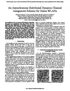
The design was motivated by the observation that instruction length decoding could pose a bottleneck in variable length instruction set architectures. As reported in [1], our analysis of the Pentium variable length instruction set revealed two principal findings (Figure 1): First, the average instruction length is about three bytes, and instructions longer than seven bytes are rare. Second, very few instruction types are used frequently. RAPPID design exploits these findings.
Length Statistics 40%
100%
30%
75%
20%
50%
10%
25%
0%
0% 2
3
1
5
4
6
7
8 10+ 9
Opcode Type Statistics 30%
100% 80%
20% 10%
60% 40% 20%
0%
0%
Figure 1: Pentium instruction set statistics; bar graphs show relative dynamic frequencies, line graphs indicate cumulative frequencies. RAPPID comprises three stages. The Length Decoder receives a sixteen-byte cache line and speculatively computes 16 instruction lengths in parallel, assuming that each byte starts a new instruction. A Tag Unit in the first byte of an instruction passes a tag downstream to the first byte of the next instruction; 4x16 Tag Units are interconnected in a torus. The instructions are routed on four separate 62-bit crossbar channels to the output. In the rest of this paper we present the RAPPID
microarchitecture, explain the design methodology, compare RAPPID to a contemporary clocked design, and discuss the risks versus rewards.
2. RAPPID microarchitecture and basic operation RAPPID receives 16-byte wide instruction cache lines at its input, extracts the instructions, and places each instruction separately in the output buffers. As shown in Figure 2, sixteen parallel length decoders are employed, which speculatively compute the length as if a new instruction began at each byte position. A torus-like distributed tagging and crossbar switching circuit with 16 columns and 4 rows packs the bytes into instructions and steers them into four output buffers. These dimensions are designed to balance the average computation rates.
The input FIFO The Input FIFO (IF) holds 16-byte wide input cache lines. The FIFO is an instruction delivery mechanism designed to operate faster than the length Decode and instruction steering Unit (DU). Keeping instruction delivery off the critical path allows us to measure unbiased maximum DU performance. The FIFO is asynchronous, but its implementation details are not described here, as it is used only as an interface to the tester. Since RAPPID decoding operation is faster than the tester’s ability to supply new data, the data, once loaded in the FIFO, are re-circulated. The FIFO is loaded serially through a scan register. Once the FIFO is filled, RAPPID operation starts, and the lines are read from the FIFO. The FIFO can be read cyclically, enabling continuous operation for performance measurements. The FIFO contains instruction bytes, and three additional bits for each byte, indicating whether this byte is used (U), whether it is the first byte of a predicted taken branch instruction (B), and whether it is a branch target (T). The prediction and target bits are derived from the BTB (branch target buffer). If a line contains a predicted taken branch, the bytes following the end of the branch instruction up to the end of the line and from the beginning of the next line, which contains the branch target, up to the branch target are marked unused, i.e., their U bits are cleared. The first line after reset starts at the first byte (byte 0).
Input FIFO (IF) Decode and Steer Unit (DU)
Byte CTRL
2 3 4
5
6
7
8
9 10 11 12 13 14 15
Row 0
Tag Unit (TU)
Row 1
Length Decode (LD)
Tag Unit (TU)
Row 2
(BC)
1
Byte Latch
Tag Unit (TU)
Row 3
Byte Unit (BU)
Column 0
Tag Unit (TU)
Crossbar Switch (XB)
Output Buffer
Crossbar Switch (XB)
Output Buffer
Crossbar Switch (XB)
Output Buffer
Crossbar Switch (XB)
Output Buffer
Figure 2: RAPPID microarchitecture Every byte in the IF is controlled separately, so the IF effectively consists of sixteen separate 11-bit wide parallel FIFOs. This structure allows the individual bytes to be transferred to the DU when needed, without having to wait for the DU to accept the next line in full.
The Length Decoding and Steering Unit The core of RAPPID is the Length Decoding and Steering Unit (DU). The DU consists of 16 identical blocks, or columns, one for each input byte, and four output buffers. Each column consists of a Byte Unit (BU), comprising the Byte Latch, Byte Control, and Length Decoder, and four identical Tag Units (TU) and Crossbar Switches (XB). The Length Decoder implementation is optimized for common instructions, such that length decoding for common opcodes is faster than for rare ones [1]. The TUs and XBs are arranged in 16 columns and four rows, wrapped around in a torus. Each XB in the four rows is connected to an output buffer. Each column receives a byte from the instruction line at the head of the IF, latches it in the Byte Latch, and performs a speculative length decoding assuming that an instruction starts at that byte. Each TU waits for the following three events to occur (See Figure 4): 1. TAGIN: A tag arrives from one of the neighboring
columns upstream. INSTRDY: Length calculation for the column is completed and the instruction is ready, meaning that all the instruction bytes are ready in their Byte Latches. 3. XBRDY: The XB of the row is ready to accept a new instruction. Once these three events occur, which may happen in any order, the tagged TU performs the following three operations in parallel: 1. Sends the tag to the TU in the column of the next instruction’s first byte in the next row. 2. Transfers the instruction bytes, along with additional information on the length and prefixes, to its row’s XB, which in turn forwards them to the output buffer. 3. Notifies its column’s BU that the instruction has been transferred from the Byte Latch to the XB. That is, once the (speculative) length calculation has been completed at the column receiving the tag and the XB in the row of the receiving TU is ready (INSTRDY and XBRDY have been asserted), the next tagged TU can immediately perform the above three operations. When a BU is notified by one of its four TUs that the instruction has been transferred to the XB (operation 3 above), it opens its Byte Latch, which permits decoding of the next instruction to begin if it is available. The BU also 2.
notifies the other BUs containing the remaining bytes of this instruction that they may open their Byte Latches. In this way, the length decoding (which is a long latency operation) of bytes from the next cache line starts as soon as the bytes from the previous line have been consumed. The columns and rows are arranged in a torus. Hence each row is a ring around that torus. As the tag wraps around the torus and crosses from column 15 back to column 0, it falls to the next row. TUs in the fourth row send the tag to the first row. The operation would be balanced if the tagged column had decoded the length of the instruction by the time the tag reaches it. Similarly, the corresponding XB would have had to complete the transfer of the previous instruction before the tag reaches it. Thus, in a perfectly balanced situation, the TAGIN, INSTRDY, and XBRDY events would occur simultaneously. Unfortunately, this is not always the case because the latency of length decoding depends on the opcode, and special case handling of branches, long instructions and prefixes incurs a longer latency. The following example demonstrates the path of the tag through the TUs, assuming a sequence of 3-byte long instructions, as shown by the arrows in Figure 2: Column 0 row 0 È column 3 row 1 È column 6 row 2 È column 9 row 3 È column 12 row 0 È column 15 row 1 È column 2 row 2 È …
•
The length decoding and instruction ready cycle. This cycle accepts a byte from the IF, decodes the instruction length (as all necessary bytes become available), and generates the Instruction Ready flag (based on the calculated length and the Byte Ready bits from the Byte Latches of the remaining bytes in the instruction). • The steering logic cycle. This cycle aligns instruction bytes from the Byte Latches and forwards them to the output buffer over the XB. • Tag cycle. This cycle directly forwards the tag to the start of the next instruction, and also synchronizes and orders the above two cycles. Each cycle has its characteristic latency that can be independently optimized based on performance targets. The length decoding cycle is optimized for common instructions [1]. The tag cycle is optimized for common lengths, as discussed below. The steering logic cycle is matched to the throughput and latency of the output buffers. We can compose these cycles, using asynchronous protocols, in a scaleable fashion to achieve the target system performance. This architecture is scaleable in both the horizontal (length decoding cycle) and vertical (steering logic cycle) dimensions. We can increase the performance through additional parallelism to achieve target performance.
Balanced design. RAPPID’s operation consists of independent self-timed cycles. The major cycles are (see Figure 3):
LENGTH DECODING CYCLE
TAG CYCLE
STEERING LOGIC CYCLE
From Input FIFO
16 byte columns Each operating at 0.72 GOPS average rate Combined average rate 0.72x16=11.5 GOPS On average, 5 instructions / cache line Effective average rate 0.72x5=3.6 GIPS
...
16x4=64 Tag units Combined rate 3.6 GIPS 4-step top-down cycle at 0.9 Cycles/nS On average, 5-step left-right cycle at 0.72 Cycles/nS 4 output buffers Each operating at 0.9 GIPS Combined rate 3.6 GIPS
Figure 3: RAPPID computation cycles and execution rates Each cycle is balanced if the function can complete just before its results are required. The cycle times are determined by the scale and wrap factors. Assuming an
average instruction length of three, each 16-byte cache line holds about five instructions. Therefore the length decoding and tag cycles are balanced if the TAGIN to
TAGOUT latency is one fifth of the decoding latency. The XB latency is four times the tag cycle latency, hence the TU and XB rows are scaled to four instances to keep the steering logic cycle balanced relative to the other two. RAPPID was designed to minimize the TAGIN to TAGOUT latency (and hence the tag cycle time); the other two cycles were scaled to match the average tag cycle time. These three intertwined cycles demonstrate one advantage of the asynchronous solution. The TAG cycle achieves the average rate of 3.6 GIPS (close to 4.5 GIPS in some of the tests, as reported below), consuming on average 720M cache lines per second. Lines with fewer than five instructions (average length greater than three bytes) are consumed faster, whereas lines with shorter instructions are consumed slower. The tag cycle, being a central point of gathering and distributing instructions, is the performance-critical component in this architecture. The steering logic cycles are shielded from variations in the length decoding cycle by the tag cycle. The Length Decoder is optimized for common opcodes, based on our benchmark analysis, which indicates that 15% of the decoding PLA minterms are used 90% of the time. The length decoding for common opcodes is done using domino logic; furthermore, the decoding of the most common opcodes is pushed closer to the outputs [1]. The rare opcodes are decoded using a slower, self-timed NOR-NOR PLA. Handling long instructions. RAPPID’s DU is optimized for instructions up to seven bytes long, which constitute 99.8% of the cases. Longer instructions (up to 11 bytes) are handled through a separate, slower protocol. Thus, each TU can tag the seven TUs in seven neighboring columns downstream in the next row down, and be tagged by any of the seven TUs in the seven neighboring columns upstream in the previous row up. The tags are sent via dedicated point-to-point lines. There are seven tag lines at the input and output of each TU. Instructions longer than seven bytes are transferred to two XBs and output buffers in two consecutive rows. The first four bytes of the instruction (head) are transferred to the XB in the row containing the tagged TU for the instruction’s first byte, and the remaining bytes (tail) are transferred to the XB in the next row down. When the calculated length is greater than seven, the Byte Control signals the columns containing the fifth byte of the instruction, through three dedicated lines, that it holds the first byte of the instruction’s tail. The fifth byte’s Byte Control modifies the length to 4, 5, 6, or 7, based on the three bits received from the first byte’s column (for total instruction length of 8, 9, 10, or 11, respectively), and sends an acknowledgment to the first byte’s column. Upon receiving this acknowledgment, the first byte’s
column modifies the Length Decoder’s output to four. The tagged TU in that column then operates as if the instruction length were four. Four bytes are transferred to the XB (together with an indication that it is the head of a long instruction), and the tag is sent to the TU in the fifth byte’s column, in the next row down. The fifth byte’s column operates as if it were the first byte of a short instruction. It transfers the tail to the XB in the tagged TU’s row, and sends the tag to the first byte of the next instruction. Instruction prefix bytes, including length-modifying prefixes, are handled in a similar manner. Handling branch instructions. When a cache line contains a predicted taken branch instruction, the tag should be routed from the TU of the branch instruction’s first byte to the TU of the branch target’s first byte. The target always resides in the next cache line (since the fetch unit is designed to fetch the target cache line of predicted taken branches), so the bytes in between the branch and the target instruction are skipped. The first bytes of the branch and target instructions are marked in the input FIFO with B and T bits, respectively, and the unused bytes in between the branch and target instructions have their used (U) bits reset. The B and T bits from the Byte Latch are routed to all four TUs in that column. When a branch instruction is tagged, the corresponding TU does not forward the tag to the first byte following its length since that byte may not be the start of the target instruction. Instead, a special tag is sent to the next row that asserts the INJECT signal. Each row has a local INJECT signal that is routed to all TUs in that row. When a row’s INJECT signal and a column’s T bit are asserted, a tag is generated for that TU and the row’s INJECT signal is de-asserted. This forwards the tag from the branch to the target instruction without tagging intermediate bytes. From that point onward, the operation continues normally. The logic generating the B, T, and U bits is not implemented in RAPPID. They are supplied pre-decoded in the IF.
3. RAPPID circuits We briefly describe two principal RAPPID circuits. The Tag Unit circuit demonstrates the use of pulse logic and reduced handshake, whereas the Byte Control circuit provides some insight into the complexity of the design.
The Tag Unit circuit The Tag Unit (TU) is responsible for transferring the tag from the column containing the first byte of an
instruction to the column containing the first byte of the next instruction. There are seven TagIn inputs to each TU, and seven TagOut outputs (Figure 4). Additionally, special TagIn and TagOut lines are used for branch handling. Transferring the tag to the next TU involves a full request-acknowledge handshake cycle when using speedindependent protocols. This means that for each of the seven TagOut outputs there should be a TagOutAck acknowledge signal. Such a structure would significantly complicate and slow down the TU logic and wiring. In order to simplify the implementation, the TagOut signals are implemented as self-timed pulses, eliminating the need for acknowledgment signals. The pulsed implementation is correct only under the following timing assumptions [2, 3]: • When a TU sends the tag pulse to the next TU, the receiving TU is ready to accept it, i.e. the selfresetting signal TagArrived (Figure 4) is off, • The TagOut pulse is wide enough to cause the state transition in the receiving TU, i.e. the TagArrived signal becomes asserted, and • The TagOut pulse is narrow enough such that it is de-asserted before the TagArrived indication in the receiving TU is de-asserted. The first assumption is satisfied by the microarchitecture. When a TU sends the tag downstream, it resets its internal TagArrived indication. The next time this TU can receive a tag is after the tag has wrapped around. The tag should make at least four hops (over the four rows) before returning to the same TU. This delay can be guaranteed to be longer than the time it takes to reset the TagArrived indication. The second and third assumptions are satisfied by careful circuit design. The TagOut outputs are generated from the TagArrived indication, which is in turn generated by a self-resetting circuit. InstRdy XBRdy
Length1 Length2
TagIn1 TagIn2 TagIn7
TagOut1 TagOut2
TagArrived Length7
TagOut7
Figure 4: Tag Unit circuit (partial diagram, not showing branch control lines)
This timed circuit was “hand-designed” with the Relative Timing methodology [3] and time-verified in part with ATACS [4]. The circuits implementing the handshake interfaces between the TU, the Byte Control and the Crossbar were also optimized using similar timed circuits and Relative Timing methodology.
Byte Unit circuit The Byte Unit is shown in Figure 5. The Byte Latch is a simple transparent latch. Length decoding may require, for some instructions, bits from the following three bytes. In addition, if a length-modifying prefix byte precedes the instruction, or if the byte is part of a long instruction, additional control bits from upstream are required. The length decoder produces seven one-hot encoded length bits. The Byte Controller FSM (BC) acknowledges the IF as soon as an incoming byte is latched. If the byte is marked unused, the BC issues a pulse on the ByteRdy line. Otherwise, it closes the latch and initiates length decoding (by asserting the LatchDecode signal), and asserts (nonpulsed) ByteRdy. The InstructionReady FSM (IR) waits for both the locally decoded length and the ByteRdy signal from L-1 neighboring columns downstream (if the locally decoded length is L), before generating InstRdy for the TU. Once a tag arrives at the column (TagArrived in Figure 4 is set) the length decoder is notified (this signal is needed for handling prefixed and long instructions). Furthermore, once the tag is sent out (one of the TagOut signals in Figure 4 is set), implying also that all bytes of the present instruction have been steered out through the XB, the AckGen FSM (AG) instructs IR and BC to get the new byte. IR then sends the corresponding Preempt signals (acknowledging ByteRdy) downstream to the remaining bytes of the instruction so that the length decoders for these columns can abort and reset upon receiving the Preempt signals. At the (non-first-byte) columns that do not receive the tag, the LDs may output the length code and the IRs may generate InstRdy. However, as soon as Preempt is received (after signaling ByteReady), the BU is reset. The control circuits in BU were designed using the 3D synthesis tool [5, 6] and optimized using the Relative Timing methodology [3]. The actual circuit employs some pulsed signaling and partial handshakes.
8+TB=10b r
a u Byte ld Control (BC)
ByteRdy
Latch / decode
Byte Latch 8b
ack
Length Decoder (LD) handshake re prefix and long instructions
7 One Hot
Preempt from 6 up nbrs
ByteRdy from 7 dwn nbrs
...
...
Ack Gen (AG)
InstRdy Control (IR)
...
ByteRdy
8 Bytes from 7 3 dwn nbrs 2 Handshake re prefix and long instructions 8+TB=10b
Preempt to 6 dwn nbrs
InstRdy Tag arrived
TagOut
Figure 5: Byte Unit circuit
4. RAPPID test results and comparisons RAPPID silicon arrived in May 98 (the layout is shown in Figure 6). It tested successfully, and the results are explained and analyzed below.
Performance RAPPID’s measured decoding and steering performance is in the range of 2.5-4.5 instructions per nanosecond. This is approximately three times the performance of a synchronous three-issue design clocked at 400MHz that achieves a peak decoding and steering performance of 1.2 instructions per nSec. RAPPID’s performance is very data dependent, and these results are valid for an average instruction stream containing common instructions of up to seven bytes long. RAPPID is not optimized for uncommon instructions, and the effects of rare, long, branch and prefixed instructions on performance are not reported. Note that RAPPID’s steering logic issues four instruction streams rather than
three, so the comparison is not completely fair. RAPPID’s performance was measured at nominal Vcc (1.8V) and Temperature, while performance for clocked design includes Vcc and temperature margins. However, it is not necessary to add the margins to RAPPID, since asynchronous circuits actually work faster in a system if the Vcc and temperature conditions are more favorable. This is in contrast to synchronous parts, which are limited by the system clock. RAPPID was tested at varying levels of Vcc for a subset of the instructions, and was determined to be operational in the range 1.0-2.0V. The part was not tested above 2.0V. The latency from the Byte Latch to the Output Buffer for common length-two instructions has been found to be only 42% that of the 400MHz clocked circuit. The main reasons for the reduced latency are the absence of clock boundaries at which the fast data must wait, and the fact that the instructions are transferred directly to the Output Buffers through the XB switches. In a clocked design with a multiple issue rate the first instruction becomes ready before the last, due to the serial nature of length decoding, but it still has to wait for the clock edge before the next
pipe stage can process it. In the asynchronous implementation, every instruction is transferred as soon as it becomes available and the time for which an instruction waits is not frequency dependent. 8 COLUMNS
4 Tag Unit and X-Bar Switch rows
Length Decoder and column control
Input FIFO (32 lines)
8 COLUMNS
Table 1 contains performance measurements for some individual instructions. Tests X0-X8 use different mixes of length-one and length-two instructions. These nine tests consist of a single 16-byte wide cache line with 0 to 8 length-two instructions followed by 16 to 0 length-one instructions (test Xi consists of i length-two instructions followed by 16-2i length-one instructions). The lengthtwo instructions in the X tests were of the type wherein the length can be determined by examining the first byte. Test I0 consists of eight length-two instructions, where the second byte is a ModR/M byte, which complicates length calculation [7]. A timing problem (setup time at the length decoder input) restricted full use of the input FIFO in some cases, so we opted to use a single cache line. The single cache line is repeatedly read from the head of the input FIFO, keeping the FIFO loop off the critical path. The tests used to measure the power also contributed to the performance measurements. The measured performance numbers were correlated with the COSMOS switch-level, unit-delay simulator, and found to have an excellent correlation. This enabled us to estimate the performance of tests that failed on silicon.
Figure 6: RAPPID layout (3.1×3.5mm)
Test X0 X1 X2 X3 X4 X5 X6 X7 X8 I0 Poweri1 Poweri2 Powerf Mix0 Mix1 C34 C223
Throughput [Inst./nSec.] 4.42 4.41 4.39 4.48 4.44 4.34 4.21 4.12 4.00 3.29 2.44 2.49 2.93 3.48 3.35 3.10 3.65
Silicon/ COSMOS Si Si Si Si Si Si Si Si Si Si COSMOS COSMOS COSMOS COSMOS COSMOS COSMOS COSMOS
No. Of Instructions 16 15 14 13 12 11 10 9 8 8 74 72 81 77 98 5 6
No. of Lines 1 1 1 1 1 1 1 1 1 1 21 20 26 14 18 1 1
Table 1: RAPPID performance tests
Test Description 16 Length 1 1 Length 2, 14 Length 1 2 Length 2, 12 Length 1 3 Length 2, 10 Length 1 4 Length 2, 8 Length 1 5 Length 2, 6 Length 1 6 Length 2, 4 Length 1 7 Length 2, 2 Length 1 8 Length 2 8 Length 2 w/ModRM 1st Integer power test 2nd Integer power test FP Power test Length 1-5 mix Length 1-7 mix 4 Length 3, 1 Length 4 2 Length 2, 4 Length 3
Power RAPPID power measured on silicon is compared to the simulated power of the logic performing the length decoding (marking) and instruction steering for a comparable clocked circuit. The comparison was made using the integer power test from the Pentium power test suite. The results show that RAPPID consumes about one half the energy as the clocked design. Since execution times differ greatly between these designs, we calculated the energy required to execute one loop of the test program. The FIFO was placed in a mode where it would not cycle the instructions. This permitted us to avoid aliasing our power results with the high energy FIFO circuit but limited us to evaluating a single cache line at a time. Therefore we measured the power of each instruction individually. The inner loop of the Pentium integer power test contains ten instructions, so we generated ten separate tests, each measuring the power of one of the instructions. Each such test consists of one instruction from the Pentium test padded by length one instructions to the end of the line. Knowing the power consumed by the length one instruction, we could calculate the power for individual instructions and the complete test suite. These results compare processors executing at different speeds and only compare a single test; a more accurate comparison should include a powerperformance curve over a larger instruction mix, which is beyond the scope of this research. RAPPID was not optimized for low power, and its superior efficiency is due only to its asynchronous design and our specific asynchronous design methodologies. In particular, data (instruction bytes) are not moved around unless necessary; they are stored only once, in the Byte Latch.
Area RAPPID’s area is compared to the area of a circuit performing the similar functionality designed on the same 0.25µ process. Apple-to-apple area comparison is difficult because of the different requirements, performance, and microarchitecture. The principal sources of inaccuracy are: 1. The three issue instruction steering logic in the clocked design contained considerably more functionality than the comparable four issue circuit in RAPPID. 2. Significant differences existed between the floorplans. 3. RAPPID doesn’t handle the instruction pointer, illegal opcodes, bogus branches, and has only
length-modifying prefix handling. Some of the clocked circuits contain unrelated logic, and isolating the relevant parts is difficult. 5. RAPPID layout is not optimized for density due to resource limitations. Our analysis shows that RAPPID consumes 22% larger area than the clocked design. This is a very reasonable area penalty for the improvements in throughput, latency and power. In conclusion, our analysis indicates that there is no evidence for a large area penalty inherent to asynchronous design. 4.
Testability Testability is considered a major potential risk for asynchronous circuits, mainly because the production testers are clock-based, and the tested devices have to exhibit a clock accurate behavior. A chip that includes an asynchronous unit does not behave in this way. Two common ways to work around this problem are to surround the asynchronous unit by a scan register and test it using Built-In Self Test (BIST), and to use only test vectors which are known to exhibit predictable behavior with respect to the clock. For fully asynchronous chips, a new type of tester will be required. Another testability issue in self-timed circuits, wherein the correct behavior of the circuit depends on relative delays, is that there may be faults that are not represented or are not detectable using the common stuck-at fault and delay models. In RAPPID we used a BIST approach in which we created a cellular automaton to feed vectors to RAPPID [8]. A signature analyzer is placed on the output to observe the signal states. The output signals and some input signals were connected to the signature analyzer. One modification was made to the cellular automaton to test for two-opcode instructions which were too rare to be generated by the automaton. A similar modification is required to generate sequences of prefixes, but was not implemented. The BIST logic was not implemented on silicon due to schedule constraints. It was designed at schematics level, and simulated using COSMOS switch-level fault simulator. Faults were injected in one column only, and only in one of the Tag Units in this column, in order to keep runtime reasonable. We expect the coverage for all blocks to be nearly identical independent of their position in the array. The stuck-at fault coverage for the Tag Unit was 98.6%, after eliminating the untestable weak feedback faults in the domino keepers. The corresponding coverage for the rest of the column (Length Decoder and Byte Control) is 91.2%, lacking mainly because the prefix handling logic was not exercised. Analysis of the undetected faults revealed an interesting type which is
specific to self-timed circuits. These circuits include some transistors which are there in order to allow the circuit to function correctly under a range of delays on gates and wires. These transistors may become redundant under a specific assignment of delays, as is the case with the unit delay model in COSMOS. This is an issue for production testing as well, since the condition at test time may be different than required for detecting the fault. We observed some undetected faults that are due to a redundant transistor under the circuit’s relative delays.
Silicon debugging Debugging an asynchronous circuit on silicon without direct probing may be an issue since the circuit is selftimed, and one cannot stop the clock and scan-out the state signals. This is especially true with the self-resetting pulsed circuits used in RAPPID, since by the time the circuit stops, the signals have already returned to their initial states. A special debug feature was designed in RAPPID to facilitate silicon debugging. Eight bits in the scan-in chain are dedicated to this feature. Each bit, when set, blocks the resetting of an internal state signal. Additional logic required to implement this blocking is minimal. In most cases, it required adding just one input to an already existing gate. All these additions were done off the critical paths, since the reset path is usually noncritical. The frozen state signals were then scanned out and observed. The debugging logic enabled us to identify three different timing-related failures of the first silicon we received in a very short time. We made a quick fix for one of them, which proved to be correct and allowed us to test the device.
5. Discussion We summarize some of our key observations below. In the early design stage, we learned how to optimize asynchronous circuits mainly for high performance at the microarchitecture level: • Optimize for the common cases: We optimized the tagging circuit for up to seven bytes and the length decoder for common instructions [1]. • Employ timing assumptions, direct signaling and pulsed logic to avoid the full handshake overhead [3]. • Use a one-hot domino circuit with automatic completion detection, e.g., for the length decoder. • Scalable parallel operation can balance the various operational rates for performance: We used four rows of tagging units and output buffers to match tagging time to the instruction steering time. • Preempting asynchronous circuits is possible: We
employed it in the length decoder to restart the decoding in non-first-bytes, as well as in case of prefixes and long instructions. • Synchronization that requires wide inefficient gates can at times be deferred by splitting the design into concurrent paths and moving the synchronization to a less expensive location. For example, RAPPID does not synchronize all sixteen bytes at the input; rather, the bytes proceeds along concurrent paths, and only get synchronized at the most opportune time by the Tag Units. In the later stages of the design, key observations were mostly related to methods for asynchronous control circuit optimizations [3]: • Relative timing assumptions were used to simplify the control circuits thus increasing their performance. • Relative timing assumptions were added to the formal verification tool ANALYZE. • Pulsed pipeline control simplified the circuit and increased performance. • Footed rather than unfooted domino may yield a faster circuit due to relaxed race conditions. Self-timed circuits are a potential solution to future design problems like delay variations and clock distribution. We are investigating the adaptive synchronization scheme for communication among units on chip in the presence of large clock skew [9] and a scheme to embed self-timed modules without significant latency penalty in globally synchronous systems [10]. We are also designing a complete CAD system for timed circuit design [11, 12, 13], and are working on Design for Testability (DfT) solutions for the undetectable faults in self-timed circuits. Such CAD and design techniques are a potential solution to the issues we will face in the future, given current trends of increasing clock frequency, interconnect delays, and delay variations.
6. Conclusion Our aggressive design methodology for asynchronous systems has resulted in a circuit that achieves three times the performance of its high-performance commercial synchronous counterpart, incurring half the latency and consuming half the power, at a comparable silicon area. We have found that the main limitation to exploiting this potential is the lack of appropriate CAD tools.
Acknowledgments We’d like to thank the many people who contributed to the RAPPID design. Kimann Truong was in charge of the
layout, together with Ken Beveridge, Ron Bean, and Roger Hill. P. Pal Chaudhury (IIT) developed the BIST logic. Henrik Hulgaard (Danish Technical University) contributed to RAPPID’s timing analysis. Intern students Wei-chun Chou, Peter Yeh, John Perry, Ayoob Dooply, and Rajesh Pendurkar participated in the design. Manpreet Khaira, Rob Roy, Niraj Bindal, Mandar Joshi, and Steve Burns provided critical help in the last phase of the project. Special thanks to Bob Bock, Mike Rhodehamel, and Manfred Wiesel who made the RAPPID silicon possible.
References [1]
[2]
[3]
[4]
W. Chou et al., Average-case optimized technology mapping of one-hot domino circuits, Proc. 4th Int. Symp. Advanced Research in Asynchronous Circuits and Systems, San Diego, CA, March 1998, pp. 80-91. V. Narayanan, B.A. Chappell and B.M. Fleischer, Static timing analysis for self-resetting circuits, Proc. Int. Conf. Computer Aided Design (ICCAD), 1996. K. Stevens, S. Rotem and R. Ginosar, Relative timing, Proc. 5th Int. Symp. Advanced Research in Asynchronous Circuits and Systems, Barcelona, Spain, April 1999. C. J. Myers. Computer-aided synthesis and verification of gate-level timed circuits, PhD thesis, Dept. of Electrical Engineering, Stanford University, October, 1995.
[5]
[6]
[7] [8]
[9]
[10]
[11]
[12]
[13]
K. Y. Yun and D. L. Dill, Automatic synthesis of extended burst-mode circuits: part I (specification and hazard-free implementations), IEEE Trans. ComputerAided Design of Integrated Circuits and Systems, vol. 18, no. 2, pp. 101-117, Feb. 1999. K. Y. Yun and D. L. Dill, Automatic synthesis of extended burst-mode circuits: part II (automatic synthesis), IEEE Trans. Computer-Aided Design of Integrated Circuits and Systems, vol. 18, no. 2, pp. 118132, Feb. 1999. Intel Corporation, Pentium-II User Reference Manual. P. Pal Chaudhury et al., Additive Cellular Automata Theory and Applications, Vol. I, IEEE Computer Society Press, June 1997. R. Ginosar and R. Kol, Adaptive synchronization, Proc. Int. Conf. Computer Design (ICCD), Austin, TX, Oct. 1998, pp. 188-190. K. Y. Yun and A. E. Dooply, Optimal evaluation clocking of self-resetting domino pipelines, Proc. 1999 Asia and South Pacific Design Automation Conference, Jan. 1999, Hong Kong, pp. 121-124. W. Belluomini and C. J. Myers, Verification of timed systems using POSETS, Int. Conf. on Computer Aided Verification, ICCAD, Springer-Verlag, 1998. R.A. Thacker, W. Belluomini, and C. J. Myers, Timed circuit synthesis using implicit methods, 12th VLSI Design Conference, Jan. 1999. H. Zheng, Specification and compilation of timed systems, Master’s thesis, University of Utah, 1998.