What, Why, and Implications for Design Automation. André DeHon and John Wawrzynek. Berkeley Reconfigurable, Architectures, Software, and Systems.
Reconfigurable Computing: What, Why, and Implications for Design Automation Andr´e DeHon and John Wawrzynek Berkeley Reconfigurable, Architectures, Software, and Systems Computer Science Division University of California at Berkeley Berkeley, CA 94720-1776
contact:
�������� �� � Reconfigurable Computing is emerging as an important new organizational structure for implementing computations. It combines the post-fabrication programmability of processors with the spatial computational style most commonly employed in hardware designs. The result changes traditional “hardware” and “software” boundaries, providing an opportunity for greater computational capacity and density within a programmable media. Reconfigurable Computing must leverage traditional CAD technology for building spatial designs. Beyond that, however, reprogrammablility introduces new challenges and opportunities for automation, including binding-time and specialization optimizations, regularity extraction and exploitation, and temporal partitioning and scheduling.
��������������� ������� Traditionally, we either implemented computations in hardware (e.g. custom VLSI, ASICs, gate-arrays) or we implemented them in software running on processors (e.g. DSPs, microcontrollers, embedded or general-purpose microprocessors). More recently, however, Field-Programmable Gate Arrays (FPGAs) introduced a new alternative which mixes and matches properties of the traditional hardware and software alternatives. Machines based on these FPGAs have achieved impressive performance [1] [11] [4]—often achieving 100 � the performance of processor alternatives and 10100 � the performance per unit of silicon area. Using FPGAs for computing led the way to a general class of computer organizations which we now call reconfigurable computing architectures. The key characteristics distinguishing these machines is that they both:
� �
can be customized to solve any problem after device fabrication
single-chip silicon die capacity grows, this class of architectures becomes increasingly viable, since more tasks can be profitably implemented spatially, and increasingly important, since post-fabrication customization is necessary to differentiate products, adapt to standards, and provide broad applicability for monolithic IC designs. In this tutorial we introduce the organizational aspects of reconfigurable computing architectures, and we relate these reconfigurable architectures to more traditional alternatives (Section 2). Section 3 distinguishes these different approaches in terms of instruction binding timing. We emphasize an intuitive appreciation for the benefits and tradeoffs implied by reconfigurable design (Section 4), and comment on its relevance to the design of future computing systems (Section 6). We end with a roundup of CAD opportunities arising in the exploitation of reconfigurable systems (Section 7).
�
��� � �"!#����$&%'�)(+*,��-.�/!#� � $102*43��������"5�%6� (�78$ 9:3;�"���"5
When implementing a computation, we have traditionally decided between custom hardware implementations and software implementations. In some systems, we make this decision on a subtask by subtask basis, placing some subtasks in custom hardware and some in software on more general-purpose processing engines. Hardware designs offer high performance because they are:
� �
customized to the problem—no extra overhead for interpretation or extra circuitry capable of solving a more general problem relatively fast—due to highly parallel, spatial execution
Software implementations exploit a “general-purpose” execution engine which interprets a designated data stream as instructions telling the engine what operations to perform. As a result, software is:
�
exploit a large degree of spatially customized computation in order to perform their computation
This class of architectures is important because it allows the computational capacity of the machine to be highly customized to the instantaneous needs of an application while also allowing the computational capacity to be reused in time at a variety of time scales. As
�
flexible—task can be changed simply by changing the instruction stream in rewriteable memory
�
relatively slow—due to mostly temporal execution relatively inefficient–since operators can be poorly matched to computational task
Figure 1 depicts the distinction between spatial and temporal computing. In spatial implementations, each operator exists at a different point in space, allowing the computation to exploit parallelism to achieve high throughput and low computational latencies. In temporal implementations, a small number of more general compute resources are reused in time, allowing the computation to be implemented compactly. Figure 3 shows that when we have only
Spatial Computation
Temporal Computation
B
B
X A
X
X
< 1 =?> F@ C
HI�����"����JK7#��9&$
Instruction binding time is an important distinction amongst these three broad classes of computing media which helps us understand their relative merits. That is, in every case we must tell the computational media how to behave, what operation to perform and how to connect operators. In the pre-fabrication hardware case, we do this by patterning the devices and interconnect, or programming, the device during the fabrication process. In the “software” case, after fabrication we select the proper function from those supported by the silicon. This is done with a set of configuration bits, an instruction, which tells each operator how to perform and where to get its input. In purely spatial software architectures, the bits for each operator can be defined once and will then be used for a long processing epoch (Figure 2). This allows the operators to store only a single instruction local to the compute and interconnect operators. In temporal software architectures, the operator must change with each cycle amongst a large number of instructions in order to implement the computation as a sequence of operations on a small number of active compute operators. As a result, the spatial designs must have high bandwidth to a large amount of instruction memory for each operator (as shown in Figures 1). Figure 4 shows this continuum from pre-fabrication operation binding time to cycle-by-cycle operation binding. Early operation binding time generally corresponds to less implementation overhead. A fully custom design can implement only the circuits and gates needed for the task; it requires no extra mem-
Binding Time:
LCustom MGate VLSI
Array
One Time Prog.
mask
metal masks
fuse program
N first
N fabrication
FPGA
Processors
load config.
every cycle
time
Figure 4: Binding Time Continuum ory for instructions or circuitry to perform operations not needed by a particular task. A gate-array implementation must use only pre-patterned gates; it need only see the wire segments needed for a task, but must make do with the existing transistors and transistor arrangement regardless of task needs. In the spatial extreme, an FPGA or reconfigurable design needs to hold a single instruction; this adds overhead for that instruction and for the more general structures which handle all possible instructions. The processor needs to rebind its operation on every cycle, so it must pay a large price in instruction distribution mechanism, instruction storage, and limited instruction semantics in order to support this rebinding. On the flip side, late operation binding implies an opportunity to more closely specialize the design to the instantaneous needs of a given application. That is, if part of the data set used by an operator is bound later than the operation is bound, the design may have to be much more general than the actual application requires. For a common example, consider digital filtering. Often the filter shape and coefficients are not known until the device is deployed into a specific system. A custom device must allocate general-purpose multipliers and allocate them in the most general manner to support all possible filter configurations. An FPGA or processor design can wait until the actual application requirements are known. Since the particular problem will always be simpler, require less operations, than the general case, these post-fabrication architectures can exploit their late binding to provide a more optimized implementation. In the case of the FPGA, the filter coefficients can be built into the FPGA multipliers reducing area [2]. Specialized multipliers can be one-fourth the area of a general multiplier, and particular specialized multipliers can be even smaller, depending on the constant. Processors without hardwired multipliers can also use this trick [6] to reduce execution cycles. If the computational requirements change very frequently during operation, then the processor can use its branching ability to perform only the computation needed at each time. Modern FPGAs, which lack support to quickly change configurations, can only use their reconfiguration ability to track run-time requirement changes when the time scale of change is relative large compared to their reconfiguration time. For conventional FPGAs, this reconfiguration time scale is milliseconds, but many experimental reconfigurable architectures can reduce that time to microseconds.
OP#� 'Q�����$6 ���;���"54*R3��� $ As we have established, instructions are the distinguishing features of our post-fabrication device organizations. Mapping out this design space, instruction organization plays a large role in defining device density and device efficiency. Two important parameters for characterizing designs in this space are datapath width and instruction depth.
S������"3�����QUTV���;��QXW�Y[Z
How many compute operators at the bitlevel are controlled with a single instruction in SIMD form? In Y processors, this shows up as the ALU datapath width (e.g. E 32 and 64), since all bits in the word must essentially perform the same
Datapath Width (w) 1 1 4
4
16
64
256 1024
FPGA Reconfigurable
2048
Processors
Media:
‘‘Software’’
Instruction Depth (c)
‘‘Hardware’’
Figure 5: Datapath Width Space
�
\
SIMD/Vector Processors
Instruction Depth Architectural Design
operation on each cycle and are routed in the same manner to and from Y memory or register files. For FPGAs, the datapath width is one ( E 1) since routing is controlled at the bit level and each FPGA operator, typically a single-output Lookup-Table (LUT), can be controlled independently. Sharing instructions across operators has two effects which reduce the area per bit operator: � amortizes instruction storage area across several operators � limits interconnect requirements to word level However, when the SIMD sharing width is greater than the native operation width, the device is not able to Y fully exploit all of its bits must all do the potential bit operators. Since a group of same thing and beY routed in the same direction, smaller operations will still consume bit operators even though some of the datapath bits are performing no useful work. Note that segmented datapaths, as found in modern multimedia instructions (e.g. MMX [7]) or multiguage architectures [10], still require that the bits in a wideword datapath perform the same instruction in SIMD manner.
�����]���.�� �������^S�$ 3���Q_W.` Z
How many device-wide instructions do we store locally on the chip and allow to change on each operating cycles? As noted, FPGAs store a single instruction per bit operator ` ( E 1) on chip allowing them to keep configuration overhead to a minimum.` Processors typically store a large number of instructions on chip ( E 1000–100,000) in the form of a large instruction cache. Increasing the number of on chip instructions allows the device capacity to be used instantaneously for different operations at the cost of diluting the area used for active computation and hence decreasing device computational density. Figure 5 shows where both traditional and reconfigurable organizations lie in this slice of the post-fabrication design space. Figure 6 shows the relative density of computational bit operators based on architectural parameters (see [3] for model details and further discussion). Of course, even the densest point in this postfabrication design space is less dense than custom a pre-fabrication implementation of a particular task due to the overhead for generality and instruction configuration. The peak operator density shown in Figure 6 is obtainable only if the stylistic restrictions implied by the architecture are obeyed. As noted, if the actual data width is smaller than the architected data width, some bit operators cannot be used. Similarly, if a task has more cycle-by-cycle operation variance than supported by the architecture, operators can sit idle during operational cycles contributing to a net reduction in usable operator density. Figure 8 captures these
Processor
128 Datapath Width (w) 64
L2 Cache
16 I−Cache
4
uP
D−Cache
MMU
Reconfigurable Array Block
1 Memory Block
1/2 1/4 Density 1/8 1/16 1/32 1/64 1/128 1
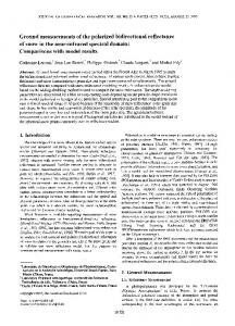
Figure 7: Heterogeneous Post-Fabrication Computing Device including Processor, Reconfigurable Array, and Memory
4 16 Instruction Depth (c)
64 256 1024
Figure 6: Peak Density of Bit Operators in Design Space
Y � `
Architectural
sequencing [8]. Mixing custom hardware and temporal processor on ASICs is moderately common these days. Since reconfigurable architectures offer complementary characteristics, there are advantages to adding this class of architectures to the mix, as well.
c effects in caricature by looking at the efficiency of processor and FPGA architectures across different task requirements. In summary, the benefits of reconfigurable architectures are: 1. greater computational density than temporal processors 2. greater semantic power, fine grained control over bit operators, for narrow word machines 3. reuse of silicon area on coarse-grain time scales 4. the ability to specialize the implementation to instantaneous computational requirements, minimizing the resources actually required to perform a computation
a
��$6��$����;J"$���$6�����b�� 'Q�����$' ���;��$6�
Large computing tasks are often composed of subtasks with different stylistics requirements. As we see in Figure 8, both purely FPGA and purely processor architectures can be very inefficient when running tasks poorly matched to their architectural assumptions. By a similar consideration, a post-fabrication programmable device, spatial or temporal, can be much less efficient than a pre-fabrication device which exactly solves a required computing task. Counterwise, a pre-fabrication device which does not solve the required computing can be less efficient than a post-fabrication device. Consider, for example, a custom floating-point multiplier unit. While this can be 20 � the performance density of an FPGA implementation when performing floating-point multiplies, the floating-point multiplier, by itself, is useless for motion estimation. These mixed processing requirements drive interest in heterogeneous “general-purpose” and “application-specific” processing components which incorporate subcomponents from all the categories shown in Figure 3. In terms of binding time, these components recognize that a given application or application set has a range of data and operation binding times. Consequently, these mixed devices provide a collection of different processing resources, each optimized for handling data bound at a different operational time scale. Figure 7 shows an architecture mixing spatial and temporal computing elements; example components exhibiting this mix include Triscend’s E5, National Semiconductor’s NAPA [9], and Berkeley’s GARP [5]. Berkeley’s Pleiades architecture combines custom functional units in a reconfigurable network with a conventional processor for configuration management and operation
d"�����"� $feg�;5�5 ��-.�"�+e4�"�]�/hid��"��� �� ���������Ueg� �"J����"9:9&�"����5 ���/j
Two major trends demand increased post-fabrication programmability. 1. greater single chip capacity 2. shrinking product lifetimes and short time to market windows
k#��$6����$����]����J�5 $& 'Q���3f )�"3��� ���/j
Large available, single-chip silicon capacity drives us towards greater integration yielding Systemon-a-Chip designs. This integration makes sense to reduce system production and component costs. At the same time, however, system designers loose the traditional ability to add value and differentiate their systems by post-fabrication selection of components and integration. As a result, monolithic System-on-a-Chip designs will require some level of post-fabrication customization to make up for “configuration” which was traditionally done at the board composition level. Further, the larger device capacity now makes it feasible to implement a greater variety of tasks in a programmable media. That is, many tasks, such as video processing, which traditionally required custom hardware to meet their demands can now be supported on single-chip, post-fabrication media. The density benefit of reconfigurable architectures helps expands this capacity and hence the range of problems for which post-fabrication solutions are viable.
7#��9&$ h�����hmlX� �oni$6��p�q�� -.$srtj' 65 $
Post-fabrication customizable parts allow system designers to get new ideas into the market faster. They eliminate the custom silicon design time, fabrication time, and manufacturing verification time. The deferred operation binding time also reduces the risk inherent in custom design; the customization is now in software and can be upgraded late in the product development life cycle. In fact, the late binding time leaves open the possibility of “firmware” upgrades once the product is already in the customer’s hands. As markets and standards evolve the behavior and feature set needed to maintain a competitive advantage over competitors changes. With post-fabrication devices, much of this adaptation can be done continually, decoupling product evolution to please market requirements from silicon design spins.
Y FPGA E ` E Design w
Y E
1
128 64
Design w
16 4
1
1.0
0.8
Efficiency
128 64
16
4 1.0
Processor ` 64, E 1024
1
0.8
0.6
Efficiency
0.6 0.4
0.4
0.2
0.2
1
1
4
4
16
16 Cycle-by-cycle Operation Variation
64
Cycle-by-cycle Operation Variation
256
64 256 1024
1024
Figure 8: Yielded Efficiency across Task–Architecture Mismatches
u�vw3;3;�"�����;��������$6� Reconfigurable architectures allow us to achieve high performance and high computational density while retaining the benefits of a post-fabrication programmable architecture. To fully exploit this opportunity, we need to automate the discovery and mapping process for reconfigurable and heterogeneous devices. Since reconfigurable designs are characteristicly spatial, traditional CAD techniques for logical and physical design (e.g. logic optimization, retiming, partitioning, placement, and routing) are essential to reconfigurable design mapping. Three things differ: 1. Some problems take on greater importance–e.g. since programmable interconnect involves programmable switches, the delay for distant interconnect is a larger contribution to path delay than in custom designs; also, since latencies are larger than in custom designs and registers are relatively cheap, there is a greater benefit for pipelining and retiming. 2. Fixed resource constraints and fixed resource ratios–in custom designs, the goal is typically to minimize area usage; with a programmable structure, wires and gates have been pre-allocated, so the goal is to fit the device into the available resources. 3. Increased demand for short tool runtimes–while hardware CAD tools which run for hours or days are often acceptable, software tools more typically run for seconds or minutes. As these devices are increasingly used to develop, test, and tune new ideas, long tool turn-around is less acceptable. This motivates a better understanding of the tool run-time versus design quality tradeoff space. The raw density advantage of reconfigurable components results from the elimination of overhead area for local instructions. This comes at the cost of making it relatively expensive to change the instructions. To take advantage of this density, we need to: 1. Discover regularity in problem–the regularity allows us to reuse the computational definition for large number of cycles to amortize out any overhead time for instruction reconfiguration.
2. Transform problem to expose greater commonality– transformations which create regularity will increase our opportunities to exploit this advantage. 3. Schedule to exploit regularity–when we exploit the opportunity to reuse the substrate in time to perform different computations, we want to schedule the operations to maximize the use of each configuration. As noted in Section 3, a programmable computation needs only support its instantaneous processing requirements. This gives us the opportunity to highly specialize the implemented computation to the current processing needs, reducing resource requirements, execution time, and power. To exploit this class of optimization, we need to: 1. Discover binding times–early bound and slowly changing data become candidates for data to be specialized into the computation. 2. Specialize implementations–fold this early bound data into the computation to minimize processing requirements. 3. Fast, online algorithms to exploit run-time specialization– for data bound at runtime, this specialization needs to occur efficiently during execution; this creates a new premium for lightweight optimization algorithms. The fixed capacity of pre-fabrication devices requires that we map our arbitrarily large problem down to a fixed resource set. When our device’s physical resources are less than the problem requirements, we need to exploit the device’s capacity for temporal reuse. We can accomplish this “fit” using a mix of several techniques: 1. Temporal x spatial assignment–on heterogeneous devices with both processor and reconfigurable devices, we can use techniques like hardware-software partitioning to utilize the available array capacity to best accelerate the application, while falling back on the density of the temporal processor to fit the entire design onto the device.
2. Area-time tradeoff–most compute tasks do not have a single spatial implementation, but rather a whole range of area-time implementations. These can be exploited to get the best performance out of a fixed resource capacity. 3. Time-slice schedule–since the reconfigurable resources can be reused, for many applications we can break the task into spatial slices and process these serially on the array; this effectively virtualizes the physical resources much like physical memory and other limited resources are virtualized in modern processing systems. In general, to handle compute tasks with dynamic processing requirements, we need to perform run-time resource management, making a run-time or operating system an integral part of the computational substrate. This, too, motivates fast online algorithms for scheduling, placement, and, perhaps, routing, to keep scheduler overhead costs reasonable small.
*4�"9:9&� � j Reconfigurable computing architectures complement our existing alternatives of temporal processors and spatial custom hardware. They offer increased performance and density over processors while remaining post-fabrication configurable. As such, they are an important new alternative and building block for all kinds of computational systems.
s �n'����![5 $6�"J;$ 9&$������ The Berkeley Reconfigurable Architectures Software and Systems effort is supported by the Defense Advanced Research Projects Agency under contract numbers F30602-94-C-0252 and DABT63C-0048.
yz$)-.$ � $��� $6� [1] Duncan Buell, Jeffrey Arnold, and Walter Kleinfelder. Splash 2: FPGAs in a Custom Computing Machine. IEEE Computer Society Press, 10662 Los Vasqueros Circle, PO Box 3014, Los Alamitos, CA 90720-1264, 1996. [2] Kenneth David Chapman. Fast Integer Multipliers fit in FPGAs. EDN, 39(10):80, May 12 1993. Anonymous FTP www.ednmag.com:EDN/di_sig/DI1223Z.ZIP . [3] Andr´e DeHon. Reconfigurable Architectures for GeneralPurpose Computing. AI Technical Report 1586, MIT Artificial Intelligence Laboratory, 545 Technology Sq., Cambridge, MA 02139, October 1996. . [4] Andr´e DeHon. Comparing Computing Machines. In Configurable Computing: Technology and Applications, volume 3526 of Proceedings of SPIE. SPIE, November 1998. . [5] John R. Hauser and John Wawrzynek. Garp: A MIPS Processor with a Reconfigurable Coprocessor. In Proceedings of the IEEE Symposium on Field-Programmable Gate Arrays for Custom Computing Machines, pages 12–21. IEEE, April 1997. .
[6] Daniel J. Magenheimer, Liz Peters, Karl Pettis, and Dan Zuras. Integer Multiplication and Division on the HP Precision Architecture. In Proceedings of the Second International Conference on the Architectural Support for Programming Languages and Operating Systems, pages 90–99. IEEE, 1987. [7] A. Peleg, S. Wilkie, and U. Weiser. Intel MMX for Multimedia PCs. Communications of the ACM, 40(1):24–38, January 1997. [8] Jan Rabaey. Reconfigurable Computing: The Solution to Low Power Programmable DPP. In Proceedings of the 1997 IEEE International Conference on Acoustics, Speech, and Signal Processing, April 1997. [9] Charl´e Rupp, Mark Landguth, Tim Garverick, Edson Gomersall, Harry Holt, Jeffrey Arnold, and Maya Gokhale. The NAPA Adaptive Processing Architecture. In Proceedings of the IEEE Symposium on FPGAs for Custom Computing Machines, pages 28–37, April 1998. [10] Lawrence Snyder. An Inquiry into the Benefits of Multigauge Parallel Computation. In Proceedings of the 1985 International Conference on Parallel Processing, pages 488–492. IEEE, August 1985. [11] Jean E. Vuillemin, Patrice Bertin, Didier Roncin, Mark Shand, Herv´e Touati, and Philippe Boucard. Programmable Active Memories: Reconfigurable Systems Come of Age. IEEE Transactions on VLSI Systems, 4(1):56–69, March 1996. Anonymous FTP pam.devinci.fr:pub/doc/ To-Be-Published/PAMieee.ps.Z.