Record Setting Software Implementation of DES Using CUDA Giovanni Agosta∗ , Alessandro Barenghi∗ ,Fabrizio De Santis † , and Gerardo Pelosi‡ ∗ Dipartimento
di Elettronica e Informazione Politecnico di Milano, 20133 Milano - Italy Email:{agosta,barenghi}@elet.polimi.it † Politecnico di Milano 20133 Milano - Italy Email:
[email protected] ‡ Dipartimento di Ingegneria dell’Informazione e Metodi Matematici University of Bergamo, 24044 Dalmine - Italy Email:
[email protected] Abstract—The increase in computational power of off-the-shelf hardware offers more and more advantageous tradeoffs among efficiency, cost and availability, thus enhancing the feasibility of of cryptanalytic attacks aiming to lower the security of widely used cryptosystems. In this paper we illustrate an GPU-based software implementation of the most efficent variant of Data Encryption Standard (DES), showing the performance of a software breaker which effectively exploits the multi-core Nvidia GT200 graphic architecture. The key point is to assess how well the structure of a symmetric key cipher can fit the GPU programming model and the single instruction multiple data architectural parallelism. The proposed breaker outperforms the fastest general purpose CPU-based implementations by an order of magnitude, and, due to the vast availability of GPUs on the market, the speedup translates into a sound improvement in the cost efficiency of the attack. As opposed to solutions based either on application specific or reconfigurable hardware, the proposed implementation does not require any specific technical knowledge from the attacker in order to be successfully built, once our implementation is available. This turns out in a better cost-availability tradeoff and minimizes the required setup time for such an attack to be mounted.
Keywords: Brute-force Attacks, DES, GPGPU. I. Introduction The Data Encryption Standard (DES) [1] is one of the most popular encryption algorithms, standardized by NIST in 1977 and subsequently maintained as a FIPS security primitive up to 2005, when it was retired [2], since it had been proved that the cipher could be broken via a brute force attack [3]. Even though DES was not considered safe anymore for government applications, comments had to be addressed holding that “the DES should be retained because it is widely used in the market” and “FIPS 463” and associated standards are used in the commercial world and serve important functions, including use by the entertainment industry for real-time broadcast security, illegal copy protection of files, and security of digital television signals” [2].
So, while not anymore relevant for high-security applications, DES continues to be used in many commercial applications due to backward compatibility reasons, thus living long beyond its recommended lifetime. The DES encryption primitive is still supported by most encryption suites, including OpenSSL [4]. Since DES was designed specifically for highly-optimized hardware implementations, its structure contains many operations which require computationally expensive adaptations in order to be executed by a general purpose CPU. Thus, both known brute force attacks, Deep Crack [3] and COPACOBANA [5], rely on dedicated hardware designs: the first in the form of ad-hoc ASIC chips, the second in the form of FPGA-based hardware. Special purpose hardware is, however, expensive, thus DES still remains a viable solution for short-term secrets, when the potential attacker has only access to consumer hardware and lacks the technical knowledge and skills required in order to build ad-hoc cracking solutions. The goal of this paper is to explore the viability of brute force attacks to the DES cipher with consumer grade hardware, thus removing the last technical barrier left to attack the cryptosystem. Given the amount of computation needed to mount such an attack, GPGPU boards appear as the most promising target hardware: not only these boards provide a very low cost/MIPS ratio (which is bound to drop further, given the nature of the GPU market), but they are readily available and easily programmed thanks to a developer toolkit provided by the manufacturer [6]. If a brute force attack can be mounted against DES with today’s GPUs, even if the performances of modern dedicated hardware solutions such as COPACOBANA are not reached, the fast evolution of the GPU market will provide more and more computational power in the near future, making in the end the software solution more cost efficient than comparable hardware solutions. Moreover, since there is already a widely deployed installbase of these devices, it is easy to harness, either through explicit agreement or by taking control of common desktops, a
large amount of computing devices [7]. In particular, in the second case, typical of a BotNet scenario, the legitimate owner of the hardware is not likely to discern the exploiting of its computational resources, since the bruteforce computation is run on the GPU, which is very often idle under a typical home workload. This paper is organized as follows: Section 2 introduces the DES algorithm and its highly optimized software implementation, Section 3 describes the NVidia GPU architecture and programming model. Section 4 reports the description of the specific GPU implementation of DES. Section 5 shows the performance results and presents a cost evaluation to realize a breaker using only consumer hardware. Finally, Section 6 draws our conclusions. II. DES Cipher DES is a symmetric block cipher with 64-bit block size that uses a 56-bit key. As previously mentioned, it was chosen as U.S.A. federal standard by NIST in 1977, when a 256 wide key space was deemed to be a sensible choice to make unfeasible any brute-force attack. The 56-bit key of DES is endowed with an additional parity byte to bring its size up to 64 bits. DES design consists of two parts, the encryption/decryption algorithm and the key-scheduling algorithm. It is an iterated block cipher consisting of 16 rounds, each designed with a Feistel structure and composed by bit-shuffling (P-boxes), nonlinear functions (S-boxes) and modular algebra linear transformations through exclusive-OR operations. The Feistel structure has the advantage that encryption and decryption operations are identical, thus requiring only a reversal of the key schedule. The key schedule algorithm, after an initial permutation of the key bits (Permuted Choice 1, PC-1), discards the eight parity bits and divides the key into two 28bit halves; each half is henceforth treated separately. For each subsequent round, both halves are rotated left by either one or two bits (depending on a predetermined table that specifies the rotations for each round), and then 48 subkey bits are selected through a second fixed permutation (Permuted Choice 2, PC2) taking 24 bits from the each half. A different set of key bits is used in each subkey (one for each round of the encryption/description algorithm) in such a way that each bit is used in 14 out of the 16 subkeys: sbki , i ∈ {1, . . . , 16}. Before encryption, the 64-bit plaintext is passed through an initial fixed permutation (IP), and the output is divided into two 32-bit blocks (L0 , R0 , respectively) in order to serve as input of the first round. In the first round, both the block R0 and the subkey sbk1 , are jointly evaluated by the (Feistel) F function that includes a block expansion operation to align its size to
48 bits, followed by a XOR operation between the subkey and the expanded block and eight substitutions through employing S-boxes having 6 bit input and 4 bit output. The 32-bit value output from the S-Boxes is passed through a fixed permutation (P-box). The output from the F function is XORed with L0 to produce R1 , whilst R0 is directly fed to the other input of the first round as L1 . These operations are iterated for 16 rounds, except for the fact that on the last round the left and right halves are not swapped and the result is subject to a final permutation (PI) to generate the 64-bit ciphertext. As for decryption, the only difference from encryption lies in the reverse order of the subkeys computed through the key-scheduling algorithm. The DES cipher was designed to intentionally slow down software implementations. Indeed, permutations of individual bits, or application of an arbitrary function (S-box) to six bits of one word in order to insert a four-bit result into another word, are executed quite inefficiently on a word-based general-purpose CPU. Eli Biham in [8], was the first to describe a software implementation of DES that exploits the intrinsic bit-level parallelism of the cipher. The basic idea lies in the application of the SIMD (Single Instruction Multiple Data) execution model at level of operations among the n-bit integers of a general purpose CPU. Operations among n-bit integers may be thought as executed by n virtual processors, each executing the same instruction in parallel but operating on different single bits of data. The implementation reported in [8] encodes 64 DES plaintext blocks in a non-standard way, in order to mimic a fast hardware implementation with minimum gate counting, and computes each gate function as a single instruction. It operates on 64-bit CPU as a SIMD machine with 64 one-bit processors. The execution of permutation and expansion operations do not involve any instruction but only register renaming. Instead, the substitution functions are translated in a sequence of logical operations that trace out the functionality of the logic gates used in the hardware implementation of Sboxes. Although the S-boxes are implemented in more instructions than the ones needed for the usual look-up implementation, the parallelism of this solution achieves a considerable speed up (about ×5), even considering the initial and final translation of the DES plaintext blocks in the non-standard representation used by this method. III. Overview of Compute Unified Device Architecture In recent times, Graphics Processing Units (GPUs) have been reengineered in order to be a source of computational power even for for non-graphical applications, thanks to the ongoing evolution of their programming interfaces and their appealing cost-performance figures
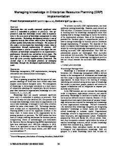
of merit. Pioneering works attempted to adapt “general purpose” applications using graphic rendering APIs (OpenGL and DirectX) since they were the only way to tap into the GPU computational resources [9]. A. The NVIDIA GT200 Architectures Modern GPUs now include hundreds of processing elements grouped in a hierarchical structure. In our case, the NVIDIA GT200 GPU series provides a set of independent multithreaded streaming multiprocessors Figure 1 shows an overview of the NVIDIA GT200 streaming processors array which is the part of the GPU architecture responsible for the general purpose computation. Each streaming multiprocessor is composed by a set of 8 streaming processors, two special functional units and a multi-threaded instruction issue unit (respectively indicated as SP, SFU and MT-Issue in Figure 1). A SP is a fully pipelined single-issue core with two ALUs and a single floating point unit (FPU). SFUs are dedicated to the computation of transcendental functions and pixel/vertex manipulations. The MT-Issue unit is in charge of mapping active threads on the available SPs. A multiprocessor is able to concurrently execute groups of 32 threads called warps. Since each thread in a warp may follow a different control flow, their execution paths may diverge due to the independent evaluation of conditional statements; in these cases the warp serially executes each path,disabling the computation for all threads that have not taken the one under execution. If the control flow ever converges back, the warp is able to return to a single, parallel execution of all threads. Each multiprocessor executes warps much like the Single Instruction Multiple Data (SIMD) paradigm, as every thread is assigned to a different SP and every active thread executes the same instruction on different data. The MT-Issue unit weaves threads into warps and schedules an active warp for execution, using a roundrobin policy with aging. Streaming multiprocessors are in turn grouped in Texture Processor Clusters (TPC). Each TPC includes three streaming multiprocessors in the GT200 architecture. Finally, the NVIDIA GPU on-board memory hierarchy includes registers (private to each SP), on-chip memory and off-chip memory. The on-chip memory is private to each multiprocessor, and is split into a very small instruction cache, a read-only data cache, and 16 KB of addressable shared data, respectively indicated as Icache, C-cache and Shared Memory in Figure 1. This shared memory is organized in 16 banks that can be concurrently accessed, each bank having a single port. B. CUDA Programming Model The Compute Unified Device Architecture (CUDA) [10], [11], proposed by NVIDIA for its G80, G92 and GT200 graphics processors, exposes a programming model that
integrates host and GPU code in the same C++ source files. The main programming introduced by the programming model is an explicitly parallel function invocation (kernel ) which is executed by a user-specified number of threads. Every CUDA kernel is explicitly invoked by host code and executed by the device, while the hostside code continues the execution asynchronously after instantiating the kernel. The programmer is provided with a specific synchronizing function call to wait for the completion of the active asynchronous kernel computation. The CUDA programming model abstracts the actual parallelism implemented by the hardware architecture, providing the concepts of block and thread to express concurrency in algorithms. A block captures the notion of a group of concurrent threads. Blocks are required to execute independently, so that it has to be possible to execute them in any order (in parallel or in sequence). Therefore, the synchronization primitives semantically act only among threads belonging to the same block. Intra-block communications among threads use the logical shared memory associated with that block. Since the architecture does not provide support for messagepassing, threads belonging to different blocks must communicate through global memory which is entirely mapped to the off-chip memory. The concurrent accesses to logical shared memory by threads executing within the same block are supported through an explicit barrier synchronization primitive. A kernel call-site must specify the number of blocks as well as the number of threads within each block when executing the kernel code. The current CUDA programming model imposes a capping of 512 threads per block. The mapping of threads to processors and of blocks to multiprocessors is mainly handled by hardware controller components. Two or more blocks may share the same multiprocessor through mechanisms that allow fast context switching depending on the computational resources used by threads and on the constraints of the hardware architecture. The number of concurrent blocks managed by a single multiprocessor is limited to 8. In addition to the logical shared memory and the global memory, in the CUDA programming model each thread may access a constant memory. An access to this read-only memory space is faster than one to global memory, provided that there is sufficient access locality since constant memory is implemented as a region of global memory fit with an on-chip cache. Finally, another portion of the off-chip memory may be allocated as a local memory that is used as thread private resource. Since the local memory access is slow, the shared memory also serves as an explicitly managed cache – though it is up to the programmer to warrant that the local
Texture/Processor Cluster
Texture/Processor Cluster
Texture/Processor Cluster
Stream Multiproc Controller
Stream Multiproc Controller
Stream Multiproc Controller Stream Multiproc
Stream Multiproc
Stream Multiproc
Stream Multiproc
Stream Multiproc
Stream Multiproc
I cache
I cache
I cache
I cache
I cache
I cache
MT issue
MT issue
MT issue
MT issue
MT issue
MT issue
C cache
C cache
C cache
C cache
C cache
C cache
SP
SP
SP
SP
SP
SP
SP
SP
SP
SP
SP
SP
SP
SP
SP
SP
SP
SP
SP
SP
SP
SP
SP
SP
SP
SP
SP
SP
SP
SP
SP
SP
SP
SP
SP
SP
SP
SP
SP
SP
SP
SP
SP
SP
SP
SP
SP
SP
SFU
SFU
SFU
SFU
SFU
SFU
SFU
SFU
SFU
SFU
SFU
SFU
Shared Memory
Shared Memory
Shared Memory
Shared Memory
Shared Memory
Shared Memory
... ... ... ... ... ... ...
Stream Multiproc
Stream Multiproc
Stream Multiproc
I cache
I cache
I cache
MT issue
MT issue
MT issue
C cache
C cache
C cache
SP
SP
SP
SP
SP
SP
SP
SP
SP
SP
SP
SP
SP
SP
SP
SP
SP
SP
SP
SP
SP
SP
SP
SP
SFU
SFU
SFU
SFU
SFU
SFU
Shared Memory
Shared Memory
Shared Memory
Figure 1. Sketch of the NVIDIA GT200 streaming processors array architecture: each Texture/Processor Cluster contains three stream multiprocessors. In turn, each stream multiprocessor is composed of eight streaming processor cores (SP), plus two special function units (SFU). Shared memory is local to each stream multiprocessor.
data being saved in shared memory are not accessed by other threads. Shared memory comes in limited amounts (threads within each block typically share 16 KB of memory) hence, it is crucial for performance for each thread to handle only small chunks of data. IV. Implementation In this section we will present the implementation strategies adopted in order to fully exploit the computational power of the nVidia CUDA architecture, and in order to perform as many DES encryptions per second as possible. Both the classical implementation and the bitsliced one have been realized in order to fully understand the extent of the speedups achievable through the exploitation of the large register file available on the graphic board, which is particularly helpful when dealing with this implementative strategies. A. Conventional DES Implementation The classical implementation of the DES algorithm we developed is aimed at exploiting the intrinsic parallelism of the brute force search of a key-space. This kind of parallelism, usually found in applications enciphering large quantity of data, such as in hard disk encryption [12], has been shown to be correctly exploitable through demanding the execution of a full encryption to a single thread. In order to sweep the full key-space, each thread thus computes Ek (P ) with a different key k, and checks the output against the correct ciphertext provided. The DES algorithm has been fully unrolled in order to avoid
control flow branches during the execution, which would have decreased the efficiency. The internal state of cipher block is represented by two 32-bit values (kept into the register file of each SM), and the swap between the two halves of the state is implemented through simple variable renaming, which has the advantage of not imposing any delay (as opposite to a real swap of values between variables). All the algorithm constants except for the S-Boxes have been hard-coded as constant values and are thus loaded with the code at no additional space cost and do not require to be stored in the global memory or in the shared memories of the graphic board. The S-Boxes are stored in the shared memory of the board and loaded from the constant memory, since the shared memory cannot be initialized statically. This incurs in a minor performance penalty only for the first call to the kernel function when the value of the SBoxes is fetched into the constant cache of the board. Since there are no other memory operations the value is stored in the caches for the whole duration of the brute-force and subsequent kernels are able to load it with a single cycle of fetching latency, for every kernel call. Avoiding to do any read/write operation from/to the main memory of the board (except for the write operation referring to discover of the correct key) allows us to fully exploit the architecture potential in terms of instructions throughput, since we do not suffer from slow loads/store operations. In order to further speedup the execution of the algorithm, the plaintext is preprocessed,
on the host side, through the initial permutation (IP), as this permutation is independent from the key. Moreover, to avoid the final permutation as well, the correct ciphertext is preprocessed, on the host side, through the inverse of the final permutation (PI−1) of the cipher: using this method, the brute-forcer can directly compare it to the output of the 16th round of the DES algorithm. Every time a kernel is launched, the host checks if the correct key has been written in a location of the board global memory in an asynchronous manner, thus without loss of performance. The location where the correct key should be written is reserved at boot-up time and is passed as a fixed parameter to the kernel. This implementation enjoy a very low occupancy of board resources, and is not expected to suffer from the simultaneous launch of a very high number of blocks or from the resource race between different warps on the same block. This considerations allows us to expect the maximum throughput for this implementation when we are employing the largest possible number of threads in flight while fitting correctly the issue window of each SM. B. Bit-sliced DES Implementation The conventional implementation is useful as a baseline for evaluating GPU-optimized implementations of DES, but it is not able to guarantee optimal performances, since the basic DES design is geared towards hardware realizations. Thus, we adopt the so-called bit-sliced algorithm [8], which is known to provide a significant performance boost when computing a large number of DES encryptions in software on 64-bit superscalar CPUs. Since the register file of the GPU is natively 32 bit wide [10], [11], we decided to perform 32 DES encryption in parallel using the bit-slicing technique. This practically means packing into a register all the n-th bits of 32 different DES encryptions (n = 0, . . . , 31), and subsequently performing all the bitwise operations of the algorithm through. This enables to successfully bypass the intrinsic slowdown due to bitwise operations which do not fit well the GPU architecture since they are transformed into bitwise operations between registers. The first step is to expand both the plaintext and the correct ciphertext into 64 register wide values, through filling a whole register with the value of every single bit of each one of them. Once this operation has been performed, the values are fixed for the whole bruteforcing effort and do not need to be changed any further. These values are placed in the shared memory of the GPU through loading them from the constant memory, since the shared memory cannot be initialized statically. In order to reduce the loading time, all the 64 values of the sliced plaintext and ciphertext are loaded in parallel, one by each thread of a CUDA-block, forcing the possible number of threads per block to be a multiple of 64.
The second step is aimed at generating keys, and test them with negligible performance losses: for the sake of clarity, we will consider the full key-space as divided into kernel sized unities, which will be swept by a single CUDA-kernel call. For the sake of clarity in the description, we split each key candidate bits into three parts and consider them as three separate indexes. This representation allows to spot out clearly which updates can be avoided during the process of generating all the possible keys (Figure 2). The first part of the key (namely, the most significant ...... 0
55 ......
Kernel Call Index
Block Index
Thread Index
[computed on host]
[computed on GPU]
[fixed]
Figure 2. Representation of the keyspace through partitioning in three separate indexes
bits) is used as a counter of the number of launched kernels, thus we need to update the value of the key slices (i.e. the values of the n-th bits of a key contained in the same register) only once every launch and this can be done easily by the host, which passes them as kernel parameters at every launch. Since these values are updated only once per kernel call, their computation is done while waiting for the previous kernel to finish, thus masking the added latency. The last part of the key (i.e. the least significant bits) is used as an index of the thread executing the enciphering operation, and is thus fixed for every block launched. This allows us to prepare all the slices regarding this part of the key in advance and pre-load them on the constant memory of the board to be further fetched with minimum overhead. The whole precomputed slice-block is very small and is below 8KB for up to 256 threads per block, thus fits the constant memory without issues. The pre-computation needed to compute these values once is negligible with respect to the time of the brute force breaking. The middle part of the candidate key bits is the only one that requires an actual computation onto the board, since it depends on which block the thread belongs to, and this is only known when the kernel is running. This computation is efficiently performed through a series of log2 (number of CUDA-blocks) binary mask operations and assignments based on the CUDA-block index, which yields the correct value for the missing slices. We stress that, regardless of which control flow path is taken through the branches which correctly select the block index in the CUDA-kernel code, the number of operations performed by each one is the same. This avoids mutual misalignments of the control flow of the different threads. This causes the minimum possible performance penalty when running the key generation code due to the
evaluation of the conditions to assign the correct values of the bits of the key slice which will be processed by a block of threads. This overhead is sensibly lower than the one which would be imposed by generating all the key slices checked by a CUDA-kernel call on the host and transferring them afterwards to the main graphic card memory, due to the high transfer latencies imposed by the PCI-Express link when copying the data. We verified experimentally that this approach impacts for less than the 1% in the execution time of the kernel. After computing the correct ones, the key-slices are stored in the registers, together with the internal state of the cipher, thus allowing the whole algorithm to be run without accessing the global memory of the board. All the permutations, expansions and selections in the DES algorithm have been eliminated through correct register renaming and the algorithm has been fully unrolled to avoid also the branching due to its round based nature. This effectively leaves only the S-Box substitutions and the key additions to be computed by the board,thus significantly lowering the number of required operations. Since the multiple memory lookup which would be involved using a tabulated form of the S-Boxes would be detrimental to performances, we employed a fully combinatorial approach to the computation of the non linear functions represented by them [13]. This approach simply considers the S-Boxes as a 6 to 4 bit generic combinatorial function whose algebraic form can be deduced through analyzing their Karnaugh maps. In order to reduce the computational impact of the S-Boxes to a minimum, we used a representation needing only 56 bitwise logical operations, which according to [13] is the most compact one when combined logical operations such as XNOR or NAND are not directly available as a single instruction from the architecture. The last thing left after computing in parallel all the encryptions is to check whether the correct key has been found. This process has been split into two parts: the comparison between the bit-sliced representation of correct ciphertext and the computed ones, and the reassembling of the results of the aforementioned comparison to extract the correct key once it has been found. The computation of all the checks for the bitsliced ciphertext is still done on the GPU since we can exploit the bit-sliced representation to check for the correctness of 32 ciphertexts at once. The results of the XOR comparison are stored in the global memory of the board and are retrieved by the host which takes care of checking if there is an actual case where the key has been found through reconstruction of the compared values. This calculation is performed while the next kernel call to the device is in flight, in order to hide the latency of the comparisons on the host which would otherwise
Table I Throughput of the standard implementation of DES (65535 CUDA-blocks per kernel) Threads per CUDA-block
Throughput [Mkey/s]
32 64 128 192 256
61.34 75.12 73.33 72.64 75.2
represent a significant slowdown. This implementation allows us to fully exploit the resources offered by the large register file on the board, we are expecting the optimal throughput to be achieved when a sufficient number of threads per block is provided in order to mask the latencies. V. Experimental Results and Cost In this section we present the results obtained with our implementation of DES and evaluate the practical feasibility of brute-force DES breaking through employing only off-the-shelf hardware which can either be bought by a single attacker or easily found in the common desktops of a group of collaborating individuals. A. Throughput Evaluation on a Single Board The evaluation campaign aimed at understanding how fast our DES implementation actually is, has been conducted on an Intel Core 2 Quad Q6600 endowed with an nVidia GeForce GTX 260 with 896MB of GDDR3. This board has 192 computing cores clocked at 576MHz and is used on a PCI-Express 1.0 bus, since the motherboard does not support the PCI-Express 2.0 specifications in full. The system is running Gentoo Linux x86 64, version 10.0 with the developer profile and the CUDA Toolkit in use is version 2.2. All the collected results have been averaged over 300 trials and consider also the time needed to transfer the data between the GPU and the host. The results on the standard implementation of DES show a steady throughput regardless of the number of blocks per kernel because of the very low occupancy of the GPU memory resources. The results presented in Table I show the maximum throughputs achievable, through calling the kernel with the maximum number of CUDA-blocks allowed (i.e. 65535), in order to minimize the overhead induced by the kernel call to the system driver. The trend varying the number of thread per blocks shows that 64 threads are sufficient in order to completely mask the access latencies to the shared memory due to the contention on the 16 read ports. Raising the number of threads per block over 64 does not yield significant performance advantages, even though the maximum throughput is reached at 128 threads per block. The maximum throughput reached is 5.6 times faster than the fastest implementation available
on general purpose CPUs , i.e. the one contained in OpenSSL [4] as shown in Table II. The results obtained 4e+08
3.5e+08
Keys/sec
3e+08
2.5e+08
2e+08
1.5e+08
1e+08
64
128
256
64 Threads/block 128 Threads/block 192 Threads/block 256 Threads/block 512 1024
2048
Number of thread blocks
Figure 3. Throughput in Mkey/s of the bit-sliced implementation of DES on an nVidia GTX 260 device with different threads configurations
from the bit-sliced implementation of DES, depicted in Figure 3, show that the number of blocks per kernel call impact significantly on the performances. This is mainly due to the more resource hungry nature of the bitsliced algorithm which thus obtains higher benefits when the graphic card is supplied with enough independent blocks to cover the latencies due to the content for the memory accesses. As far as the optimal number of threads per block goes, 256 threads per block is the most performant choice, proving that the CUDA architecture is able to deal with an increased pressure on the register file without problems, thus confirming the intuition given in [8],that architectures having a large register file are particularly well fit to run bit-slice implementations of DES. The maximum speed achieved is 373.58 Mkeys per second, which is 10 times faster than the reference bitsliced implementation available for CPUs. The reference implementation taken is is a specially crafted assembly implementation using SSE2 instructions and 128 bit registers from the Intel Pentium 4 and greater line of CPUs and is the one contained in John the Ripper [14], the state of the art brute-forcer for general purpose processors. We also notice that, in comparison with the conventional implementation on graphic cards, we achieve a 5x speedup, thus meeting the most optimistic expectations and practically proving the viability of our approach. Table II Throughput comparison of different implementations of the DES cipher on CPU, GPU and FPGA hardware
CPU GPU FPGA
DES Plain [106 key/s]
DES BS [106 key/s]
13.32 [4] 75.33 (our GTX260) 216 [5]
36.85 [14] 373.58 (our GTX260) –
B. Cost Evaluation of a Bruteforcing Cluster Given the throughput results for a single video card, let us now consider the time and financial effort that either motivated attackers or a group of common people in possession of the correct hardware for other reasons, need to invest to successfully break DES. Our aim is to evaluate the effective cost of building a cluster of simple desktops which can be used in order to break DES. To evaluate the best tradeoff in terms of computational power we assume to build PCs using common consumer grade components and to fit two video cards per computer. All the reference prices for this evaluation have been taken from online retailers, without taking into account any discount that could be obtained for a large order. The overhead needed in order to build a computer able to run our implementation of the bit-sliced DES algorithm is 177 e. Table III reports the results of our cost analysis. The first column of the table reports all the models available from the 200 series from nVidia together with the number of cores available on the single board. The second column reports the cost of a single board, together with the maximum number of instruction per second provided per unity of cost. The estimated instruction per second throughput for each card has been calculated assuming that each core is able to compute an instruction on a single clock cycle, which is a reasonable assumption in our case, since all the instruction involved in the brute-forcing are implemented in a single clock cycle within the architecture. We did not consider as a relevant feature the quantity of on board memory provided by the boards since in none of them this represents a constraint for our implementations. The most cost efficient choice for an attacker is the GTX260216, a beefed-up version of the card used in our tests, which includes an extra processor cluster and is able to provide roughly 60% more instruction per cost unit with respect to the top of the line models. Contrary to common intuition, the fastest boards do not provide the best tradeoff in terms of computing power per cost, due to the rapid price drop of older models in the video card market. The third column reports the number video cards acquirable with a budget identical to the one used to buy all the components for COPACOBANA [5] (8980e). The figures provided take into account the overhead of 177e(November 2009) needed for every two cards in order to build a working cluster. The last column reports the practical breaking time achieved on a cluster build with off the shelf hardware, using our implementation of the DES algorithm: as it can be seen, the best solution obtained is able to find a DES key in 18 days, thus proving the feasibility of such an attack. We stress that the brute-forcing power scales linearly without loss among the different machines since no
Table III Summary of the cost analysis oriented at building a DES breaking cluster with off-the-shelf components (177e overhead to build the hosts included) nVidia Video Card Model Device Cores GTX295 GTX285 GTX275 GTX260 GTX260-216 GTX250
480 240 240 192 216 128
Graphic Card Cost Cost IPS/e 308 180 136 96 110 73
Number of Video Cards Affordable with COPACOBANA budget
897.66 864.00 1117.06 1005.38 1462.50 1294.03
communication at all is required among the nodes of the breaking cluster. This breaking speed is achieved with 24 nodes of the cluster with two boards each, as reported in Table III, thus it is more than reasonable to assume that, in the case the attacker decides to exploit a number of seized machines through a BotNet (whose typical size may scale up to tens of thousands of nodes), the time needed to break a DES encryption can be brought down to a few hours, fast enough to avoid being noticed by the owners of the infected machines. The fact that the only libraries needed in order to run the cracking program are indeed the video card drivers, makes the computational resource theft even easier since every system endowed with a properly configured CUDA enabled video card can be successfully exploited without any preparation. VI. Conclusions In this paper, we propose the first GPU-based implementation of the DES encryption algorithm geared toward password breaking, and provide and experimental evaluation to prove how a single GPU outperforms a single CPU by a factor of 10. We also provide insights on the cost of practical DES breaking using our implementation, showing how, for a moderate cost (equivalent to the hardware breaker COPACOBANA) and without the need of technical expertise, we can recover a DES key in as little as 18 days. Given the commodity nature of the hardware employed in our bruteforcer, even a group of people without specific technical knowledge, but with access to typical “gamer” personal computers, could easily mount an attack against a DES-protected secret. Acknowledgements This work was partially supported by MIUR in the framework of the PRIN SESAME project. References [1] National Institute of Standards and Technology (NIST), “FIPS-46-3: Data Encryption Standard (DES),” http:// www.itl.nist.gov/fipspubs/, May 1999. [2] NIST, “Announcing Approval of the Withdrawal of Federal Information Processing Standard (FIPS) 463,” Federal Register, vol. 70, no. 96, pp. 28 907–28 908, May 2005.
22 32 40 44 48 56
DES Breaking Standard [day] Bitsliced[day] 100 122 100 125 90 115
20 24 20 25 18 23
[3] M. Loukides and J. Gilmore, Eds., Cracking DES: Secrets of Encryption Research, Wiretap Politics and Chip Design. Sebastopol, CA, USA: Electronic Frontier Foundation – O’Reilly & Associates, Inc., 1998. [4] The OpenSSL Project, “OpenSSL: The open source toolkit for SSL/TLS,” www.openssl.org, Oct. 2009. [5] T. G¨ uneysu, T. Kasper, M. Novotn´ y, C. Paar, and A. Rupp, “Cryptanalysis with COPACOBANA,” IEEE Trans. Comput., vol. 57, no. 11, pp. 1498–1513, 2008. [6] A. D. Biagio, A. Barenghi, G. Agosta, and G. Pelosi, “Design of a parallel aes for graphics hardware using the cuda framework,” in IPDPS. IEEE, 2009, pp. 1–8. [7] S.-G. Brett, C. Marco, C. Lorenzo, G. Bob, S. Martin, K. Richard, K. Chris, and V. Giovanni, “Your Botnet is My Botnet: Analysis of a Botnet Takeover,” in ACM CCS, Nov. 2009. [8] E. Biham, “A Fast New DES Implementation in Software,” in FSE ’97: Proceedings of the 4th International Workshop on Fast Software Encryption. London, UK: Springer-Verlag, 1997, pp. 260–272. [9] J. D. Owens, D. Luebke, N. Govindaraju, M. Harris, J. Kr¨ uger, A. E. Lefohn, and T. J. Purcell, “A survey of general-purpose computation on graphics hardware,” Computer Graphics Forum, vol. 26, no. 1, pp. 80–113, 2007. [10] J. Nickolls, I. Buck, M. Garland, and K. Skadron, “Scalable parallel programming with cuda,” ACM Queue, vol. 6, no. 2, pp. 40–53, Mar. 2008. [11] NVIDIA Corporation, “CUDA Technology,” http:// www.nvidia.com/CUDA, Sep. 2008. [12] G. Agosta, A. Barenghi, F. D. Santis, A. D. Biagio, and G. Pelosi, “Fast disk encryption through GPGPU acceleration,” in PDCAT. IEEE Computer Society, 2009, pp. 102–109. [13] M. Kwan, “Reducing the Gate Count of Bitslice DES,” Cryptology ePrint Archive, Report 2000/051, 2000, http: //eprint.iacr.org/. [14] OpenWall Project, “John the Ripper Password Cracker,” http://www.openwall.com/john/, Oct. 2009.