Reducing L1 Caches Power By Exploiting Software Semantics Zhen Fang
Li Zhao
Xiaowei Jiang
NVIDIA Corp.
Intel Labs, Intel Corp.
Intel Labs, Intel Corp.
[email protected] Shih-lien Lu
[email protected] Ravi Iyer
[email protected] Tong Li
Intel Labs, Intel Corp.
Intel Arch. Group, Intel Corp.
Intel Labs, Intel Corp.
[email protected]
[email protected] Seung Eun Lee
∗
[email protected]
Seoul National University of Science and Technology
[email protected] ABSTRACT
1.
To access a set-associative L1 cache in a high-performance processor, all ways of the selected set are searched and fetched in parallel using physical address bits. Such a cache is oblivious of memory references’ software semantics such as stack-heap bifurcation of the memory space, and user-kernel ring levels. This constitutes a waste of energy since e.g., a user-mode instruction fetch will never hit a cache block that contains kernel code. Similarly, a stack access will not hit a cacheline that contains heap data. We propose to exploit software semantics in cache design to avoid unnecessary associative searches, thus reducing dynamic power consumption. Specifically, we utilize virtual memory region properties to optimize the data cache and ring level information to optimize the instruction cache. Our design does not impact performance, and incurs very small hardware cost. Simulations results using SPEC CPU and SPECjapps indicate that the proposed designs help to reduce cache block fetches from DL1 and IL1 by 27% and 57% respectively, resulting in average savings of 15% of DL1 power and more than 30% of IL1 power compared to an aggressively clock-gated baseline.
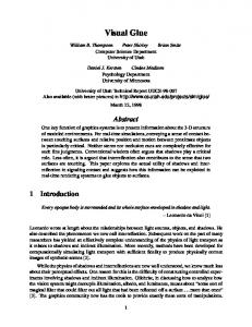
In a general-purpose processor, the first level cache is one of the most critical units: it has to both meet performance requirement and fit into the processor’s power envelope. Most of the architecturelevel power optimizations to caches have been designed for L2/L3 caches where slightly lengthened hit latencies and/or decreased hit rates are acceptable. However, these compromises are usually not acceptable for the L1 cache in a high-performance processor. Some of the power efficiency improvement techniques proposed for L1 caches [4, 6, 10] were adopted by earlier microprocessors. But latest commercial processors (Intel Nehalem/Sandy Bridge/Atom, IBM Power7[13], etc.), though more power-aware than before, have abandoned those designs in the L1 cache due to the hardware complexity they introduce and risks of lengthening the read hit cycle. In this study, we take a novel approach to save the power consumption of the set-associative L1 cache without lengthening its access cycle or decreasing the hit rate. Specifically, we observe that a significant portion of the parallel accesses to the data/tag stores are unnecessary because many of the ways do not contain data whose software semantics are compatible with the memory request. By exploiting software semantics in the L1 cache design, we eliminate these unnecessary activities. The benefit is reduced dynamic power consumption in instruction fetches and data loads. The semantics that we will be using are 1) virtual memory, and 2) privilege ring levels. Before we proceed to details of the proposed mechanism, we provide background on L1 caches in high-performance processors, as well as both software semantics. Background on High-Performance L1 Caches L1 caches in high-performance processors have been aggressively optimized to achieve low latency for hits. Fig. 1 shows a representative timing diagram of a read hit in a physically-tagged set-associative L1 cache. Because the cache tags use physical address bits, tag comparison cannot start until the TLB has completed virtual-to-physical address translation. To meet the tight timing target, in an N-way set-associative L1C, all N data blocks of the selected set are accessed in parallel, irrespective of the tag lookup result. At least N-1 blocks will be discarded later, resulting in low power efficiency. This is different than L2/L3 or low-power caches where tag check and data readout are serialized. L1 data and instruction caches of literally all modern general-purpose microprocessors are implemented in this manner. Bifurcation of the Virtual Memory Space Figure 2(a) shows a representative virtual memory map. The bifur-
Categories and Subject Descriptors B.3.2 [Memory Structures]: Design Styles
General Terms Design, Power, Performance
Keywords First-level cache, virtual memory, ring level, simulation ∗This work was done when all authors were employed by Intel.
Permission to make digital or hard copies of all or part of this work for personal or classroom use is granted without fee provided that copies are not made or distributed for profit or commercial advantage and that copies bear this notice and the full citation on the first page. To copy otherwise, to republish, to post on servers or to redistribute to lists, requires prior specific permission and/or a fee. ISLPED’12, July 30–August 1, 2012, Redondo Beach, CA, USA. Copyright 2012 ACM 978-1-4503-1249-3/12/07 ...$10.00.
BACKGROUND AND MOTIVATION
CLK
N ways of data all fetched in parallel
phy tag
TLB
At least N-1 blocks will be discarded
hit/miss
VA
Tag array
Tag cmp
way_sel Way mux
Data array
Word
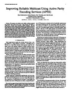
Figure 1: Read Pipeline in a High-Performance L1 Cache cation design implies that in the virtual address space, the most significant bit (MSB) can differentiate stack and heap regions. However, this semantic is completely lost in the physical memory space, due to the way that the operating system manages page frames. Figure 2(b) shows that on average, about 40% of all data memory references are accesses to the stack. The rest of the 60% consists of accesses to the heap, BSS and data segments, with heap being the dominant component. In the rest of the paper, we use the term ‘heap’ to refer to all three non-stack segments – heap, BSS and data. Although the stack accounts for 40% of all memory instructions, on average it only occupies 20% of the capacity on a 32KB, 8-way setassociative L1 data cache (DL1), as a result of the stack’s relatively small footprint[7].
tradicting one’s intuition. In equake, 76% of the cachelines actually contain kernel code. The phenomenon can be explained by the different characteristics of kernel and user programs. User code usually spends the majority of the time in nested loops, while the OS is more likely to traverse non-iterative decision trees, occupying more I-cache entries. The tight loops in user code such as SPEC CPU benchmarks, on the other hand, have rather small static instruction memory sizes; user application execution tends to repeatedly fetch instruction from some hot ways of hot sets, which allows the (rarely used) kernel code to stay for a long time before being evicted. I-caches do not take advantage of ring level information. Though a user-mode instruction fetch will never hit a cacheline that contains kernel-mode code, all ways in the selected cache set are still searched in parallel. For example, based on the profiling data of equake in Figure 3, statistically about (1-2%)×76%+2%×(1-76%)=75% of all accesses to I-cache RAMs will result in tag mismatches and fetched instruction blocks being discarded. This observation motivates our optimization to the instruction cache. 100%
100%
Cachelines w/ Kernel Code / All Cachelines Kernel Instr / Total Instr
80% 0xFFFFFFFF 0xC0000000
Kernel Space
Stack
Upper half of VM (MSB = 1)
80% Stack Accesses Count
Stack Data Occupancy
K-instr occup = 16% 60% K-instr count = 3%
60%
60% 40%
40%
40%
20%
20%
AVG
vpr
twolf
swim
mgrid
parser
mesa
gcc
mcf
gap
gzip
art
eon
0% apsi
Data Code
20%
equake
0x0
Lower half of VM (MSB = 0)
bzip2
BSS
applu
Heap
K-instr occup = 76% K-instr count = 2%
(a) gcc
0x80000000
Shared Libs
(b) equake 80%
0%
0% 1
401
801
1201 1601 2001 2401 2801 3201
Time (x 25 u-seconds)
(a) Linux Addr Map (b) Stack Access Count and Avg Occupancy
1
401
801
1201 1601 2001 2401 2801 3201
Time (x25 u-seconds)
Figure 3: Kernel Code’s Instr. Counts and Occupancies
Figure 2: Virtual Memory Map and Characteristics Ring Levels and Instruction Cache Sharing Ring level is a mechanism by which the operating system (OS) and the processor hardware cooperate to restrict what user-mode programs can do. All mainstream processors use similar mechanisms. For brevity, we base our discussion on the x86 architecture. When a user (kernel) program executes, the processor is set to the least (most) privileged level, ring 3 (ring 0). Rings 1 and 2 have been largely unused except by virtualization layers. The processor’s current ring level is stored in the 2-bit CPL field of the Code Segment register. User applications and the OS do not share code, but they share the instruction cache. There has been a number of work studying interaction of OS and microarchitecture[1, 9, 11]. They provide data on overall instruction count and cache miss rates of kernel and user codes, for example. One question remains unanswered – at any given time, what percentage of the I-cache capacity is used by kernel code? One’s intuition would suggest that in compute-intensive applications the I-cache be constantly filled with user application code, interfered only occasionally by kernel instructions brought in by events like system calls. We found that this intuition is not correct. Figure 3 shows histograms of dynamic instruction counts and occupancies of kernel-mode code in steady stages of two SPEC CPU benchmarks on a 32KB, 8-way L1 instruction cache (IL1). Each data point represents the average value in an interval of 25 µseconds. In each figure, we also give the algebraic mean values of both bands of data averaged over the 3400 intervals. As can be seen, although user code dominates instruction count, kernel instructions occupy a significant portion of the I-cache, clearly con-
2.
TAGGING CACHELINES WITH SOFTWARE SEMANTICS
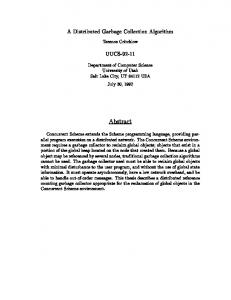
We propose to exploit software semantics in the cache design to avoid unnecessary associative searches, thus reducing dynamic power consumption. We present two software semantics-aware cache designs, for the data cache and instruction cache, respectively. In both designs, further search operations in the cache set are continued only if the semantic tag comparison gives a match. Vtag (1 bit per cacheline): Tag each L1 data cacheline with virtual memory region information. Using the most significant bit of the virtual address can help to eliminate all the cross-checks between stack and heap data. Rtag (2 bits per cacheline): Tag each L1 instruction cacheline with ring level information, represented by the processor’s ring level status bits when the instruction is fetched and cached. For a user-level instruction fetch, this obviates the need to search the ways that contain kernel-level code, and vice versa. A key advantage of the semantic tag over the physical tag is that the former can be checked concurrently with virtual-to-physical address translation, avoiding performance impact typically seen in a phased-access cache [6].
2.1
Augmenting DL1 with Vtags
Fig. 4 shows an implementation of a 32KB, 8-way L1 data cache augmented by Vtag. Thick lines denote new logic that we propose to add. The virtual page number is translated by the TLB to a physical page number, which will serve as the physical tag. When the N (N=8 in our example) tags are fetched out of the tag store, they are
all compared with the incoming physical tag, and at most one comparison can be a hit. Data store accesses are performed in parallel with the N tag store accesses. From AGU/ MOB
VPN[MSB:12]
index[11:6]
offset[5:0]
bits of the processor while Vtag uses the highest order virtual address bit of the incoming request. One would derive an implementation of Rtag-augmented IL1 from Vtag in DL1. Fig. 6(a) shows how such a design can reduce accesses to the data store in a 4-way set-associative instruction cache. In such a design, similar to the Vtag case, we can not optimize IL1 tag array and ITLB accesses.
set TLB
V-tag
Tag
Way 1 Data
…
Tag
Way N Data
PPN 512b
512b
u
k
WS
WS
W1
W2
W3
Way selects (WS) generation is on critical path of tag access. word
hit?
Figure 4: Eliminating Unnecessary DL1 Data Array Accesses using Vtags. Selective data readout from the SRAM arrays is realized by qualifying WL/BL operations with Vtag check results, eliminating unnecessary bitline discharges. In a traditional cache, all N data subbanks have to be accessed. In a Vtag-optimized cache, we implement selective data readout from the SRAM arrays. To achieve this, we augment each cacheline with the most significant bit of its virtual address. When a data read arrives, Vtag check is performed in parallel with TLB access, in addition to the regular physical tag check. Data subbank i (1 ≤ i ≤ N) is accessed only if Vtag check = match for way i. The largest components of cache power dissipation, bitline discharge and sense amps ops, are eliminated for the Vtag mismatching ways. The Vtag design does not require changes to cache hit assertation and does not affect coherency protocols. Optimizing tag array accesses and DTLB is challenging because of the tight timing constraints. So regular physical tag check is performed regardless of whether Vtag is a hit or a miss. Fig. 5(a) shows the optimized DL1 pipeline for a read hit. Using the example in Fig. 4, the Vtag logic consists of reading from a 64-bit store for each of the N subbanks followed by 1-bit XOR. We implemented the Vtag logic in 32nm CMOS technology. It can be completed in well under 0.08 nanoseconds. This gives enough time to propagate the way selection signals to the data store since it is in parallel with TLB look up. This extra delay will fit into the first phase of the clock even with frequency up to 4GHz. Address Aliasing Address aliasing refers to a special scenario in memory management where two virtual pages point to a same physical page. With respect to address aliasing, the Vtag mechanism does not change the cache’s behavior except when a high virtual page and a low virtual page are backed by a same physical page. False match by Vtags will not occur since physical tag comparison is still performed. False miss, however, could occur and cause program execution errors. Because creation of an aliased mapping is performed by the OS memory manager, the OS can simply disable Vtag usage when such a mapping is created, and thus avoid false misses. Since intentional address aliasing is rare in practice (unintentional aliasing would indicate a bug in the OS), for the vast majority of applications, the Vtag feature will not need to be disabled.
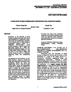
Augmenting IL1 with Rtags
Conceptually, instruction cache’s Rtag optimization is similar to data cache’s Vtag optimization, except that Rtag uses the ring level
u
u
Bitmask of set i 0
k WS
0
Data W0
data WL/BL enable
k
WS
=
V-tag hit
2.2
u
current mode: u
WS
=
Ring-level vector of set i
Ring-level vector of set i k
current mode: u
(a) Basic Implementation
1
1
0
W0
1
WS
W1
1
WS
W2
0
WS
W3
Tags and Data
Bitmask of set i
WS generated by the LRU logic in the last miss to the set.
Generation of the bitmask
No Rtag comparison after set selection
Usage of the bitmask
(b) Optimized Implementation
Figure 6: Using Rtags to Optimize ICache/ITLB Accesses In Fig. 6(b), we present a better solution which removes ringlevel check from the critical path of IL1 and ITLB tag array accesses. We make an observation that dynamically generating ring level match signals for every instruction fetch is not necessary, because these signals for a cache set do not change unless a cacheline replacement occurs in the set, or if the ring level of the current thread changes. We introduce a bitmask for each set, in addition to the ring level Rtag vector. The bitmask directly serves as way selection to enable/disable wordlines and bitlines. The left half of Fig. 6(b) illustrates how a bitmask is generated, while the right half shows how it is used. The bitmask generation and usage are decoupled. Compared with Fig. 6(a), the key difference is that Rtag comparison is performed when a cacheline is installed, not when it is looked up. When a cache set is selected by the indexing logic for an IL1 read, its bitmask is ready to use, without the need for Rtag comparison. In other words, the bitmask for each cache set is generated before any read has been made to the set. Compared with the basic implementation, in the decoupled mechanism, generation of the bitmask is no longer on the critical path of tag array reads; it is done in the cache miss handling process. When the processor’s ring level changes, every bit in every bitmask is flipped. With R ring levels in the processor, the total storage size for cache_size bits and log(R) × ring levels and bitmasks is log(R) × cacheline_size Number_o f _entries bits for the I-cache and I-TLB, respectively. Assuming R = 4, 32KB IL1, 64B/line, 128-entry ITLB, total storage overhead is 1024 bits + 256 bits = 160 bytes. The power consumption overhead of such a structure is minuscule compared with the number of subbank accesses that we will be saving. Fig. 5(b) shows the pipeline of an IL1 hit with Rtag masking logic (the solid bars). The bitmask design allows us to place the Rtag check logic before IL1 physical tag and ITLB VPN processing, thus optimizing the power consumption of not only the data arrays, but also the tag arrays. A Quick Summary on the Designs Table 1 summarizes the optimizations that we have discussed. In DL1, Vtag uses a 1-bit XOR with the potential to eliminate a full cacheline data fetch. In IL1, for the vast majority of instruction fetches, Rtag uses a 1-bit way-selection mask with the potential to eliminate both the tag comparison and the data array access. Our Vtag and Rtag designs require no changes to cacheline replacement logic, does not change cache hit/miss rates, and has no impact on cache hit latency. The power consumption overhead of the new logic is minuscule compared with the number of subbank accesses that we will be saving. Being only a small extension to most L1
CLK
CLK
phy tag
TLB
TLB
hit/miss
VA
Tag array
Vtag check
Tag cmp
way_sel
Data array
Way mux
PC
Word
Tag array
phy tag reduced ways of I-tag
and I-TLB accesses hit/miss Tag cmp Data array
way_sel Way mux
Word
bitmask
reduced ways of data accesses
reduced ways of data accesses
(a) Data Cache
(b) Instruction Cache and Instruction TLB
Figure 5: Pipelines of Vtag- and Rtag-Optimized L1 Caches cache implementations in general-purpose CPUs, we believe that the total cost of commercial processor adoption is low. Table 1: Summary of cost and benefits. Storage overheads are for the entire DL1/IL1 based on an Intel Nehalem-like processor. Extra Bits Vtag: MSB of Virtual Addr Rtag: Ring Level, Bitmask
2.3
Cache
Data Array?
Overhead
DL1
Tag Array? not optimized
optimized
64 bytes
IL1
optimized
optimized
128 bytes
Qualitative Discussion on Power Savings
The effectiveness of the proposed optimizations primarily depends on the overall selectivity of the semantic tags throughout the application execution. For a cache access, selectivity is defined as the number of semantic tag matches divided by the cache associativity. For example, if the Vtag of an incoming data read matches the stored Vtags of 2 of the 8 ways in the set, the selectivity is 25% for this access. A lower selectivity value is desirable since more unnecessary data array accesses would be eliminated. For an access to a Vtag-optimized D-cache, P_DL1 = P_tag_data_lkg + P_dec + P_tag_dyn + selectivity × P_data_dyn + P_vtag_ovhd
(a)
For an access to a Rtag-optimized I-cache and I-TLB, P_IL1 = P_tag_data_lkg + P_dec + selectivity × (P_tag_dyn + P_data_dyn) + P_rtag_ovhd
(b)
When there is no access to DL1, IL1 or I-TLB, P_idle = P_tag_data_lkg + residual_factor × (P_dec + P_tag_dyn + P_data_dyn)
(c)
CMOS technology parameters, obtained through MOSIS, into Wattch. Leakage is assumed to be 20% of the overall baseline power for L1 cache, and is not optimized by our design. We calculate energy consumption of the caches using the model in Section 2.3 on a cycle-by-cycle basis and integrate the numbers to derive the average power. Table 2 shows the key simulation parameters. In particular, the L1 cache parameters are representative of the latest high-performance processors like Intel Nehalem and Sandy Bridge. Application traces of SPEC CPU2000 and SPECjappsServer04 were collected using full-system emulator SoftSDV[14] running Fedora 10. After skipping the warm-up phases, SoftSDV captured all fetched instructions and dumped them into traces. These traces faithfully contain the dynamic instruction sequence of all user and kernel instructions. In most experiments, we run each trace for 1 billion instructions in a steady stage of the applications. Table 2: Simulation setup. (Bold fonts denote default values.) Parameter Value Processor core 3.2GHz, out-of-order L1 I-cache 32KB, 64B/line. 8-way and 4-way, LRU L1 D-cache 32KB, 64B/line. 8-way and 4-way, LRU TLB Data: 96 entries, 8-way Instr: 64 entries, 8-way L2 cache 64B/line, 8-way, 4MB, LRU Latencies L1=3 cycles; L2=12 cycles. DRAM=120ns
Figure 7: Power Consumption Components. selectivity is the key parameter to be obtained through simulation.
3.2 Vtag and Rtag reduces power consumption of different structures, as is shown in Table 1. In an N-way set-associative array, accessing M of the N ways consumes approximately M/N of the baseline dynamic power by gating the clocks to the bitlines and segmented wordlines of the rest N − M subarrays. When clock gated, the cache power consists of a constant leakage power and some residual dynamic power, given in Equation (c) in Fig. 7. Aggregating Equations (a), (b) and (c) for the whole application simulation gives us the overall average power of DL1 or IL1.
3. 3.1
EVALUATION Simulation Methodology
We use a trace-driven, cycle-accurate platform simulator [16] to model the performance aspect of the architecture. To estimate power dissipation, we integrated microarchitecture-level power estimation tool, Wattch[3], into ManySim. We plugged in 45nm
Experiment Results: Vtag on DL1
We present the selectivity profiles of SPEC CPU, shown in Figure 8. The data are collected on an 8-way set-associative DL1 setup. In the figure, for each application, the four segments represent the percentages of different selectivity ranges. For example, the ’≤75%’ segment of applu has a value of 28% (the yellow portion), indicating that 28% of all L1 data cache reads’ Vtags hit either 5 or 6 of the Vtags in their respective selected sets. On average, about 19% of memory accesses have ≤25% Vtag matches in their respective cache sets, denoted by the bottom segment of the Avg bar. For these memory reads, their Vtags match 0, 1, or 2 of the Vtags in their respective selected sets. This means that for 19% of all DL1 accesses, only up to two data subbanks need to be activated on our 8-way cache. Because Vtag does not optimize write instructions, all write instructions count as 100% match in the statistics. High match percentages are usually a result of unbalanced numbers of stack/heap accesses. For example, in mcf, stack reads only