Reduction Design for Generic Universal Switch Blocks HONGBING FAN University of Victoria, Canada JIPING LIU University of Lethbridge, Canada YU-LIANG WU and C. K. WONG The Chinese University of Hong Kong
A k-side switch block with W terminals per side is said to be a universal switch block ((k, W )-USB) if every set of the nets satisfying the routing constraint (i.e., the number of nets on each side is at most W ) is simultaneously routable through the switch block. The (4, W )-USB was originated by designing better switch modules for 2-D FPGAs, such as Xilinx XC4000-type FPGAs, whereas the generic USBs can be applied in multidimensional or some nonconventional 2-D FPGA architectures. The problem we study in this article is to design (k, W )-USBs with the minimum number of switches for any given pair of (k, W ). We provide graph models for routing requirements and switch blocks and develop a series of decomposition theorems for routing requirements with the help of a new graph model. The powerful decomposition theory leads to the automatic generation of routing requirements and a detailed routing algorithm, as well as the reduction design method of building large USBs by smaller ones. As a result, we derive a class of well-structured and highly scalable optimum (k, W )-USBs for k ≤ 6, or even W s, and near-optimum (k, W )-USBs for k ≥ 7 and odd W s. We also give routing experiments to justify the routing improvement upon the entire chip using the USBs. The results demonstrate the usefulness of USBs. Categories and Subject Descriptors: B.7.1 [Integrated Circuits]: Types and Design styles—algorithms implemented in hardware; gate arrays General Terms: Design, Theory, Algorithms Additional Key Words and Phrases: FPGA architecture design, routing, routing requirement, switch module, universal switch block, decomposition
1. INTRODUCTION Switch blocks are critical components in Field Programmable Gate Arrays (FPGAs) [Brown et al. 1992; Betz et al. 1999]; they have great effects on area and time efficiency and routability of FPGA chips. We consider here a kind of Authors’ addresses: H. Fan, Dept. of Computer Science, University of Victoria, Victoria, BC, Canada V8W 3P6; J. Liu, Dept. of Mathematics and Computer Science, University of Lethbridge, Lethbridge, AB, Canada T1K 3M4; Y.-L. Wu, C. K. Wong, Dept. of Computer Science and Engineering, The Chinese University of Hong Kong, Shatin, NT, Hong Kong; email:
[email protected]. Permission to make digital / hard copy of part or all of this work for personal or classroom use is granted without fee provided that the copies are not made or distributed for profit or commercial advantage, the copyright notice, the title of the publication, and its date appear, and notice is given that copying is by permission of the ACM, Inc. To copy otherwise, to republish, to post on servers, or to redistribute to lists, requires prior specific permission and /or a fee. ° C 2002 ACM 1084-4309/02/1000-0526 $5.00 ACM Transactions on Design Automation of Electronic Systems, Vol. 7, No. 4, October 2002, Pages 526–546.
Generic Universal Switch Block Reduction Design
•
527
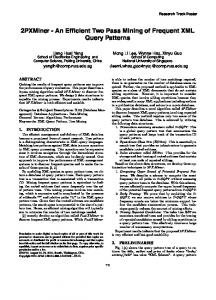
Fig. 1. The architecture of a 2-D FPGA.
switch blocks called universal switch blocks (USBs), which was first proposed in Chang et al. [1996] for four-side switch modules and proved to be a good candidate for FPGA switch blocks. The model was further generalized to k-side switch blocks for three-dimensional FPGA and various 2-D FPGA architectures in Shyu et al. [2000]. In this article, we aim to give a solution to the generic USB design problem. A conventional 2-D FPGA consists of arrays of prefabricated logic cells, connected by logic pins, routing wire segments, and user-programmable switches. Figure 1 shows the conceptual diagram of the architecture. The functional blocks (or logic cells) are marked by L, and are separated by vertical and horizontal channels. There are W (called channel density) prefabricated parallel wire segments running between each pair of adjacent L-cells in both the vertical and horizontal channels. The wire segments in a vertical (or horizontal) channel are aligned into W vertical (or horizontal) tracks; each track within a channel is assigned an integer in {1, . . . , W } as its track ID. There is a connection block (CB) between each pair of adjacent L-cells, and a switch block (SB) at each intersection of vertical and horizontal channels. Both CBs and SBs contain programmable switches connected to the terminals of wire segments associated with them. This kind of FPGA architecture has been widely investigated [Brown et al. 1992; Chang et al. 1996; Pan et al. 1998; Rose and Brown 1991; Wu and Marek-Sadowska 1997; Wu et al. 1996]. When an FPGA is used to implement a particular Boolean function, the pins used to implement the Boolean function are grouped into nets. Then the pins in each net are connected by using available wire segments and switches in both CBs and SBs; different nets are disconnected. This process is called routing, and conventionally is divided into two steps, the global router and the detailed router. The global router decides the connection topology of all the nets, and its result (usually a set of paths or trees) is called a global routing. The detailed ACM Transactions on Design Automation of Electronic Systems, Vol. 7, No. 4, October 2002.
528
•
H. Fan et al.
router decides which wire segments and switches in CBs and SBs are used to implement the connections based on the global routing. The result is called a detailed routing. The routability of an FPGA chip is measured by the probability of completing a detailed routing for a global routing. There are many issues in the design of SBs. The foremost two are the global routability and area efficiency [Brown et al. 1992; Betz et al. 1999]. The area efficiency can be characterized by the number of switches, where a small number of switches are desired. However, the high routability and high area efficiency are two conflicting goals. It is easy to see that an FPGA with complete SBs, namely, having a switch between every pair of terminals from different sides, will have the highest routability under the same channel density. But it has the lowest area efficiency and it is impractical when the channel density is large. To have a balanced SB, Rose and Brown [1991] defined an important parameter Fs , called the flexibility of a switch block, which is the maximum number of switches in an SB connecting a terminal. They investigated the effects of flexibility on the global routability and observed that Fs = 3 or 4 can result in a sufficiently high global routability, which is an acceptable trade-off between global routability and area efficiency. This raises the problem of designing SBs with flexibility 3 (or 4) while possessing high routing capacity. The universal switch block investigated in this article is a class of switch blocks with high routing capacity. The conventional SBs in a 2-D FPGA have k sides and W terminals on each side, where 2 ≤ k ≤ 4. However, researches on three-dimensional, six-way and eight-way mesh, and some other tree-structured FPGA architectures raised interest in switch block designs with k (≥5) sides and W terminals on each side ((k, W )-SB for short) [Shyu et al. 2000]. Figures 2(a), (b), and (c) show examples of (k, 3)-SBs for k = 4, 5, 6. When a net is restricted on a single SB, it specifies two sides of the SB on which a connection should be made. Such a net is, in fact, a restriction of a path of a global routing at an SB. A detailed routing of a net is an exact assignment of switches to carry out the connection required by the net. A (k, W ) routing requirement ((k, W )-RR for short) is a set of nets satisfying the density constraint; that is, the number of nets incident with each side is of at most W . Figures 2(d), (e), and (f) show examples of (k, 3)-RRs for k = 4, 5, 6. A detailed routing of a (k, W )-RR in a (k, W )-SB is an assignment of switches in the switch block such that each net in the routing requirement corresponds to a switch, and the switches corresponding to different nets are not incident. Figures 2(g), (h), and (i) show the detailed routings of the (k, 3)-RRs of (d), (e), and (f) in the (k, 3)-SBs of (a), (b), and (c), respectively. If a (k, W )-RR R has a detailed routing in a (k, W )-SB B, then we say B is routable for R, or R is routable in B. The local routing capacity of an SB is measured by the probability that a routing requirement has a detailed routing in the SB. Definition 1. A (k, W )-SB is said to be universal or it is a (k, W )-USB if it is routable for every (k, W )-RR. A (k, W )-USB is said to be optimal if it has the minimum number of switches among all (k, W )-USBs. The above concept of a universal switch block was first proposed in Chang et al. [1996]. A symmetric (4, W )-SB with flexibility 3 was defined and shown ACM Transactions on Design Automation of Electronic Systems, Vol. 7, No. 4, October 2002.
Generic Universal Switch Block Reduction Design
•
529
Fig. 2. Examples of (k, 3)-SBs, (k, 3)-RRs and the corresponding detailed routings for k = 4, 5, 6.
to be an optimum (4, W )-USB. It was also shown that the symmetric (4, W )USBs increase the local routing capacity by 25% over the disjoint switch blocks used in Xilinx XC4000 type FPGAs. The concept of the universal switch block was later extended to the hyperuniversal switch block (HUSB) [Fan et al. 2000; Fan et al. 2001a], which was defined to be routable for every multipin net routing requirement, where a multipin net specifies two or more sides on which a connection should be made. Even though no theoretical arguments prove that the local optimized USB or HUSB can result in higher global routability at chip level, extensive experiments show that both USB and HUSB do increase the global routability [Fan et al. 2001a]. The USB Design Problem. For any fixed integer k ≥ 2, design an optimum (k, W )-USB for every W ≥ 1. ACM Transactions on Design Automation of Electronic Systems, Vol. 7, No. 4, October 2002.
530
•
H. Fan et al.
For k = 4, the design problem was solved in Chang et al. [1996], where the symmetric switch modules are optimum (4, W )-USBs and the number of switches in optimum (4, W )-USBs is 6W . Shyu et al. [2000] investigated the generic USB design problem and claimed that the generalized symmetric switch module is also universal for k ≥ 5. Unfortunately, this claim is not true. Fan et al. [2001b] pointed out the error and provided a partial solution. In this article, we present a design method that derives optimum or near optimum generic (k, W )-USBs. The rest of the article is organized as follows. Section 2 presents graph models for routing requirements, switch blocks, and detailed routings. In Section 3, we provide a series of decomposition theorems, based on which we derive the routing requirement generation, detailed routing algorithm, and reduction design scheme for USBs. Section 4 shows the designs obtained by the reduction design method including a class of optimum (k, W )-USBs for all k with all even W s or for k ≤ 6 with all W s, and near optimum (k, W )-USBs for k ≥ 7 and odd W s. In order to justify how such a different switch block design can improve on the entire chip routing, we also give routing experiments for MCNC benchmarks in Section 6. The results are encouraging. Section 7 presents our conclusions. 2. GRAPH MODELS FOR USB DESIGN Graph models for routing requirements and switch blocks play an important role in our design scheme and decomposition theory. We model a routing requirement as a collection of subsets that can be viewed as a graph, and a USB as a graph with terminals as vertices and switches as edges. With these formulations, the USB design problem becomes a graph design problem, and results and notations in combinatorial theory and graph theory can be applied in USB designs. Readers are referred to Bondy and Murty [1976] for more graph theory. The first significant step of our design method is the graph modeling of the routing requirement, which is represented by the routing requirement vector (RRV) in Chang et al. [1996] and Shyu et al. [2000]. We represent a routing requirement by a collection of subsets, which can be viewed as a graph. Label the sides of a (k, W )-SB by 1, 2, . . . , k; then a net restricted on the (k, W )-SB can be represented by a size 2 subset of {1, 2, . . . , k}. For example, a net that connects two terminals on sides 1 and 2 can be represented by {1, 2}. A (k, W )-RR can be represented as a collection (multiple set) of size 2 subsets (also called nets) of {1, 2, . . . , k}, such that each i ∈ {1, 2, . . . , k} is contained in no more than W subsets in the collection. To distinguish the routing requirement and its presentation, we refer to the subset representation of a routing requirement as global routing. For the sake of regularity, we add some singletons (nets of size 1) to the collection such that each element appears the same number of times, and call it a balanced global routing (BGR), defined formally as follows. Definition 2. A collection {Ni |i = 1, . . . , v} of subsets of {1, 2, . . . , k} with |Ni | ≤ 2 for i = 1, . . . , v is said to be a k-way balanced Pv global routing (or |Ni ∩ { j }| = d for simply k-BGR) if there exists an integer d such that i=1 all j = 1, . . . , k. d is called the density of the k-BGR. A k-way balanced global routing of density d is shortened to (k, d )-BGR. ACM Transactions on Design Automation of Electronic Systems, Vol. 7, No. 4, October 2002.
Generic Universal Switch Block Reduction Design
•
531
Let R be a (k, d )-BGR and R 0 be a subcollection of R. If R 0 is a (k, d 0 )-BGR with d 0 < d , then R 0 is said to be a subglobal routing of R. R is said to be a minimal BGR (MBGR) if it contains no subglobal routing. An MBGR is also said to be nondecomposable as it can not be decomposed into (namely, represented as the disjoint union of) some k-BGRs with smaller densities. By this definition, we see that a k-BGR can always be decomposed into k-MBGRs. A (k, d )-BGR is said to be primitive if it does not contain two different singletons (i.e., all of its singletons must be located on the same side). Clearly, a subglobal routing of a k-PBGR is also a k-PBGR. Therefore, a k-PBGR can always be decomposed into k-way primitive MBGRs (k-PMBGRs). A switch block (k, W )-SB can be naturally presented by a graph as follows. Denote the j th terminal on side i by a vertex vi, j and a switch connecting vi, j and vi0 , j 0 by an edge vi, j vi0 , j 0 . Thus a (k, W )-SB corresponds to a k-partite graph G with vertex partition (V1 , . . . , Vk ), where Vi = {vi, j | j = 1, . . . , W }, i = 1, . . . , k. We refer to such a graph as a (k, W )-graph. Two (k, W )-graphs are isomorphic if there is an isomorphism that preserves the vertex partitions. A detailed routing of a net {i, j } can be represented by an edge connecting a vertex in part Vi and a vertex in part V j in the representing (k, W )-graph G; a detailed routing of a net of size one {i} can be expressed by a vertex in part Vi . Therefore a detailed routing of a (k, W )-GR in an SB corresponds to a subgraph of G consisting of a set of independent edges and vertices. If a BGR R is not primitive, then we can combine two unequal singletons to obtain a BGR with a smaller number of unequal singletons. Continuing this process, we will eventually obtain a PBGR R 0 . A detailed routing of R 0 will induce a detailed routing of R by simply deleting the edges representing the nets of size two in R 0 that are obtained by combining the unequal singletons in R. Therefore we need only consider PBGRs as routing requirements in the designing of USBs. By the above graph models, the universal switch block design problem becomes a graph design problem; that is, to design a (k, W )-graph with the minimum number of edges such that it has a detailed routing for every (k, W )-BGR (or, equivalently, (k, W )-PBGR). One of the advantages of BGR representation for routing requirements is that it can be viewed as a regular hypergraph. A hypergraph is an ordered pair (V , E) where V is a vertex set and E is an edge set consisting of a collection of subsets of V . The degree of a vertex of a hypergraph is defined to be the number of edges incident with the vertex. A hypergraph is r-regular if the degrees of all its vertices are equal to r. A hypergraph is s-bounded if the size of every edge is at most s. For convenience, we simply refer to a 2-bounded hypergraph as a 2-graph, and the edges of sizes two and one as links and singletons, respectively. An r-factor of a graph (or 2-graph) is a spanning (containing all vertices) r-regular subgraph. Thus a (k, d )-GR, a (k, d )-BGR, a (k, d )-MBGR, and a (k, d )-PBGR correspond to a 2-graph on k vertices, a d-regular 2-graph on k vertices, a d-regular 2-graph on k vertices that does not contain a proper factor, and a d-regular 2-graph on k vertices that does not contain a proper factor and does not contain two different singletons, respectively. With this graph representation, we can make use of the terminology of graph theory. For example, ACM Transactions on Design Automation of Electronic Systems, Vol. 7, No. 4, October 2002.
532
•
H. Fan et al.
we say two BGRs R1 and R2 are isomorphic if their corresponding 2-graphs are isomorphic, denoted by R1 ∼ = R2 . Another advantage of BGR is its decomposition property, which says that, for a fixed k, a k-way BGR is decomposable if the density is large enough or, equivalently, the number of k-PMBGRs is finite. In graph terminology, a d-regular 2-graph on k vertices has a proper spanning regular subgraph when d is large enough. We show that the decomposition property of BGRs plays a key role in the USB designs. It enables us to design a k-side USB of large channel density by combing a few k-side USBs of small channel densities. The following example of a (4, 4)-USB illustrates the basic idea of our reduction design method for USBs. Example. Let k = 4. It is not hard to see that there are only two nonisomorphic 4-PMBGRs; one has density 1 and the other density 2 (see 4R11 and 4R12 in Figure 4). Therefore any (4, W )-PBGR can be decomposed into (4, 1)-PMBGRs and (4, 2)-PMBGRs. They can further be grouped into (W/2) (4, 2)-PBGRs when W is even, and ((W − 1)/2) (4, 2)-PBGRs and a (4, 1)-PMBGR if W is odd. Thus we need only design a (4, 2)-USB and a (4, 1)-USB. A (4, W )-USB can be obtained by a disjoint union of W/2 copies of (4, 2)-USB when W is even, and (W − 1)/2 copies of (4, 2)-USB and a (4, 1)-USB. Figure 3(b) shows a (4, 4)-USB obtained by the union of two copies of a (4, 2)USB. Consider a (4, 4)-GR, {{1, 2}, {1, 3}, {1, 4}, {2, 3}, {2, 3}, {3, 4}}. Convert it to a (4, 4)-BGR as {{1, 2}, {1, 3}, {1, 4}, {2, 3}, {2, 3}, {3, 4}, {1}, {2}, {4}, {4}}. Then it can be transformed into a PBGR (not unique) {{1, 2}, {1, 3}, {1, 4}, {2, 3}, {2, 3}, {3, 4}, {1, 2}, {4}, {4}}. This PBGR can then be decomposed into two (4, 1)-PMBGRs {{1, 2}, {3, 4}}, {{1, 4}, {2, 3}}, and one (4, 2)-PMBGR {{1, 2}, {2, 3}, {1, 3}, {4}, {4}}. Combine the two (4, 1)-PMBGRs; then we obtain two (4, 2)PBGRs {{1, 2}, {3, 4}, {1, 4}, {2, 3}} and {{1, 2}, {2, 3}, {1, 3}, {4}, {4}}. Figure 3(a) shows the transformations of these GRs, and Figure 3(b) shows how to combine two (4, 2)-USBs to obtain a (4, 4)-USB and the corresponding detailed routings of the above two (4, 2)-PBGRs. 3. DECOMPOSITION PROPERTIES OF BGRS In this section, we first prove a fundamental decomposition theorem, then provide a method to compute all k-PMBGRs, and give a complete list of nonisomorphic k-PMBGRs for k = 1, . . . , 8. We further provide the universal decomposition theorems that are used in the (k, W )-USB designs. 3.1 The Fundamental Decomposition Theorem The following theorems are the basis of our reduction design method for USB as well as the detailed routing algorithm. THEOREM 1 [FAN ET AL. 2002]. For any given integer k, there exists a unique minimum integer f 2 (k) such that every (k, W )-BGR can be decomposed into k-MBGRs with densities at most f 2 (k). Inasmuch as there are a finite number of k-MBGRs with a fixed density and the densities of k-MBGRs are bounded by f 2 (k), we have the following. ACM Transactions on Design Automation of Electronic Systems, Vol. 7, No. 4, October 2002.
Generic Universal Switch Block Reduction Design
•
533
Fig. 3. Combining two (4, 2)-USBs into a (4, 4)-USB and a detailed routing example: (a) transformation and decomposition of PMBRRs; (b) the construction of (4, 4)-USB and detailed routing.
THEOREM 2. For any given positive integer k, the number of k-MBGRs is finite, and f 2 (k) equals the maximum density of all k-MBGRs. Since a k-MBGR can be converted into a k-PMBGR with the same density, the statements of the above theorems are also true for PMBGRs and the maximum density f 2 (k) of k-MBGRs is equal to the maximum density of all ACM Transactions on Design Automation of Electronic Systems, Vol. 7, No. 4, October 2002.
534
•
H. Fan et al.
k-PMBGRs. Therefore, to show that a (k, W )-SB is universal, we need to verify that every (k, W )-PBGR is routable. To verify this, we first need to generate all (k, W )-PBGRs, and then test if they have detailed routings. By Theorem 1, a (k, W )-PBGR can always be obtained by a combination of several k-PMBGRs. In other words, with a complete set of k-PMBGRs, we can constructively generate all (k, W )-PBGRs. We next present a complete set of k-PMBGRs with 1 ≤ k ≤ 8, and then give a method to compute k-PMBGRs in general. 3.2 Complete k-PMBGRs for 1 ≤ k ≤ 8 To simplify the representation of the complete set of k-PMBGRs, we choose one representative (as a type) from each equivalent class determined by permutations (or isomorphisms), and give a complete list of the different types. We use k Rir to denote the ith type of k-PMBGR with density r. For example, a complete list of 3-PMBGR types is 3R11 = {{1, 2}, {3}}, 3R12 = {{1, 2}, {2, 3}, {1, 3}}. A complete list of 4-PMBGR types is 4R11 = {{1, 2}, {3, 4}}, 4R12 = {{1, 2}, {2, 3}, {3, 1}, {4}, {4}}. Theorem 3 gives the values of f 2 (k) and all k-PMBGRs for 1 ≤ k ≤ 8. THEOREM 3 [FAN ET AL. 2002]. f 2 (k) = 1 for k = 1, 2, f 2 (k) = 2 for 3 ≤ k ≤ 6, and f 2 (k) = 3 for 7 ≤ k ≤ 8. The 2-graph representations of the complete lists of k-PMBGR types for 1 ≤ k ≤ 8 are given in Figure 4. 3.3 Estimation of f2 (k) The function f 2 (k) is of great importance in the computation of a complete list of k-PMBGRs. In this subsection, we provide some information about f 2 (k). All the proofs are constructive; their main idea is that starting from a 2-graph, which is a representation of a (k, d )-PBGR, a d -regular graph with the same decomposition property is constructed and, thereby, we can employ the following well-known Petersen’s Theorem in graph theory. LEMMA 4 (BONDY AND MURTY [1976, P. 7]). gree contains a 2-factor.
A regular multigraph of even de-
The following theorem shows that any k-BGR of even density ≥4 is not minimal. THEOREM 5.
The following statements hold.
(i) The density of a k-PMBGR must be either 2 or an odd number; (ii) f 2 (k + 1) ≥ f 2 (k); (iii) f 2 (k) is odd when k ≥ 7. PROOF. (i) Let G be a (k, d )-PMBGR. Then G is a d-regular 2-graph which is not decomposable. Suppose on the contrary that d is even. If G does not contain singletons, then G is a regular graph of even degree. By Lemma 4, ACM Transactions on Design Automation of Electronic Systems, Vol. 7, No. 4, October 2002.
Generic Universal Switch Block Reduction Design
•
535
Fig. 4. The complete list of different k-PMBGR types for k = 1, . . . , 8. ACM Transactions on Design Automation of Electronic Systems, Vol. 7, No. 4, October 2002.
536
•
H. Fan et al.
G would contain a 2-factor, which is a contradiction. Suppose now G has one vertex v covered by r singletons. Then we make another copy of G and joining the two vs with r edges obtain a regular graph G 0 of even degree, which contains a 2-factor by Lemma 4. The restriction of the 2-factor of G 0 on G together with a possible singleton v or two singletons of v is a 2-factor of G, which again is a contradiction. Therefore d is either 2 or an odd number. (ii) Let G be a (k, f 2 (k))-PMBGR. Adding a vertex together with f 2 (k) singletons covering the vertex to G we obtain a (k + 1, f 2 (k))-MBGR. Therefore f 2 (k + 1) ≥ f 2 (k). (iii) When k ≥ 7, f 2 (k) ≥ f 2 (7) = 3 by (ii), and f 2 (k) must be odd by (i). THEOREM 6.
f 2 (k) ≤ (k(k − 1))/2.
PROOF. By Theorem 3 it is clearly true when k ≤ 8. Now assume that k ≥ 9. Because f 2 (k) is an increasing function, we have f 2 (k) ≥ f 2 (8) = 3, and f 2 (k) is odd. Let G be a 2-graph corresponding to a k-PMBGR of degree f 2 (k). We next show that there is a nondecomposable f 2 (k)-regular graph G 0 with at most k + 3 vertices. Because G corresponds to a k-PMBGR, it has k vertices and contains at most one vertex covered by singletons. If G has no singletons, let G 0 = G. Suppose now that G has a vertex v that is covered by singletons, if v is covered by an even number, say 2r, of singletons. Then let G 0 be the graph obtained from G by adding two extra vertices x, y and r edges joining v and x, r edges joining v and y, and f 2 (k) − 2r edges joining x and y. Let v be covered by an odd number, say 2r + 1, of singletons. If f 2 (k) = 2r + 1, then delete v and let G 0 be the graph obtained by deleting v from G; otherwise, let G be the graph obtained by adding three extra vertices x, y, z and 2r + 1 edges joining v and x, ( f 2 (k) − 2r − 1)/2 edges joining x and y, ( f 2 (k) − 2r − 1)/2 edges joining x and z, and f 2 (k) − ( f 2 (k) − 2r − 1)/2 edges joining y and z. It is easy to verify that, in any case, G 0 is a nondecomposable f 2 (k)-regular graph and the size of G 0 is at most k + 3. On doubling each edge of G 0 , we obtain a 2 f 2 (k)-regular graph G 00 . By Lemma 4, we know G 00 can be decomposed into the union of f 2 (k) 2-factors G i , i = 1, . . . , f 2 (k). G i is a 2-factor of G 00 but not a 2-factor of G 0 since G 0 is not decomposable. Because every cycle of G i with length greater than 2 must be a cycle of G 0 , G i must contain a cycle Ci of length 2 which is not a cycle of G 0 . Let e be the digon edge of Ci . Then e has multiplicity one in G 0 and two in G 00 and e cannot be in G j , for j 6= i. Therefore f 2 (k) is no more than the number of edges in G 0 with multiplicity one. Then by the definition of G 0 , we know that the number of edges in G 0 with multiplicity one is at most k(k − 1)/2. Therefore f 2 (k) ≤ (k(k − 1))/2. The significance of Theorem 6 is that it enables us to compute efficiently the complete list of k-PMBGRs for any fixed k. That is, there is a polynomial time algorithm in terms of k to compute the complete list of k-PMBGRs. THEOREM 7. Let k be a positive integer with k ≥ 7. Let i = k (mod 6) when k (mod 6) 6= 0, and i = 6 otherwise. Then f 2 (k) ≥ (k + 3 − i/3). ACM Transactions on Design Automation of Electronic Systems, Vol. 7, No. 4, October 2002.
Generic Universal Switch Block Reduction Design
•
537
Fig. 5. A (6t + 1, 2t + 1)-PMBGR.
PROOF. For any positive integer t, let k = 6t + 1 and d = 2t + 1. We are going to construct a d-regular 2-graph H(d ) as follows. The vertex set is {v0 } ∪ {vi, j |i = 1, . . . , d − 1, j = 1, 2, 3}, and edge set {v0 } ∪ {v0 vi,1 |i = 1, . . . , d − 1} ∪ {vi,1 vi,2 , vi,1 vi,3 |i = 1, . . . , d − 1}(t) ∪ {vi,2 vi,3 |i = 1, . . . , d − 1}(t+1) , where S (r) denotes the multiple set of r copies of S (see Figure 5). Clearly, H(d ) is a d-regular 2-graph. We show that H(d ) does not contain any proper factor. Suppose, on the contrary, that H(d ) contains a nontrivial spanning regular subgraph G. We note that G is not a 1-factor, and at least one link edge incident with v0 is in G. Without loss of generality, assume that v0 v1,1 is in G. By symmetry, the multiplicity of v1,1 v1,2 and v1,1 v1,3 in G must be equal. This implies that the degree of v1,1 must be odd in G. G is a proper factor, therefore there must be an edge incident with v0 that is not in G. Without loss of generality, suppose that v0 v2,1 is not in G. Then {v2,1 , v2,2 , v2,3 } induces a component of G that is a regular graph of odd degree. This is impossible as the number of vertices of odd degree must be even. This shows that H(d ) represents a (6t + 1, 2t + 1)-PMBGR for any integer t. By Theorem 5(ii), f 2 (k) is an increasing function; thus f 2 (6t+6) ≥ f 2 (6t+5) ≥ f 2 (6t + 4) ≥ f 2 (6t + 3) ≥ f 2 (6t + 2) ≥ f 2 (6t + 1) ≥ 2t + 1. Let k = 6t + i. Then f 2 (k) ≥ (k + 3 − i)/3 for i = 1, 2, 3, 4, 5, 6. We believe that the lower bound for f 2 (k) given in Theorem 6 should also be an upper bound for f 2 (k). We pose the following conjecture. CONJECTURE 1. Let k ≥ 7 be a positive integer. Let i = k (mod 6) when k (mod 6) 6= 0, and i = 6 otherwise. Then f 2 (k) ≤ (k + 3 − i)/3. If this conjecture is true, then the running time for generating all k-PMBGRs will be greatly improved as we need only generate all (k, d )-PMBGRs with d ≤ (k + 3 − i)/3. ACM Transactions on Design Automation of Electronic Systems, Vol. 7, No. 4, October 2002.
538
•
H. Fan et al.
Fig. 6. Transformation of a 2-graph into a multigraph.
3.4 Universal Decomposition Theorems With the fundamental decomposition theorems, we can further obtain several decomposition properties of BGRs for USB designs. THEOREM 8. Let d be an even positive integer. Then a (k, d )-BGR can be decomposed into d /2 (k, 2)-BGRs. PROOF. For any (k, d )-BGR R, we can convert R into a (k, d )-PBGR R 0 by combining different singletons. It is easy to see that any (k, 2)-PBGR decomposition of R 0 induces a (k, 2)-BGR decomposition of R. Therefore we only need to consider (k, d )-PBGRs in the proof. Let G be a 2-graph representing a (k, d )-PBGR. If G does not have singletons, then G is a regular multigraph of even degree, and thus G has a 2-factor by Lemma 4. Let G have singletons. Then all the singletons must be equal singletons, say {x}. d is even and the degree of the vertex x is even upon deleting all the singletons. Therefore there are an even number, say 2m, of singletons. Let G 0 be the regular multigraph obtained by adding two copies of {x, y i }, (d − 2)/2 copies of { y i , z i } and { y i , wi }, and (d + 2)/2 copies of {z i , wi } for i = 1, . . . , m, where y i , z i , wi are new vertices (see Figure 6). G 0 could also be constructed as follows: add to G three new vertices { y, z, w}, 2m copies of edge {x, y}, (d − 2m)/2 copies of edges { y, z} and { y, w}, and (d + 2m)/2 copies of edge {z, w}. Clearly G 0 has degree d and therefore contains a 2-factor F by Lemma 4. Deleting all the vertices y i , z i , wi from F and adding a number of singletons {x} to make the resulting graph F 0 2-regular, F 0 is then a 2-factor of G. G − E(F 0 ) is (d −2)-regular which is of even degree; G − E(F 0 ) has a 2-factor. Continuing this process, we see that G can be decomposed into a set of 2-factors and hence a (k, d )-PBGR can be decomposed into (d /2) (k, 2)-PBGRs. THEOREM 9. hold.
Let k and d be positive integers. Then the following statements
(i) When k ≤ 6, then every (k, d )-BGR is a union of bd /2c (k, 2)-BGRs and at most one (k, 1)-PBGR. ACM Transactions on Design Automation of Electronic Systems, Vol. 7, No. 4, October 2002.
Generic Universal Switch Block Reduction Design
•
539
(ii) If k ≥ 7 and d ≥ f 2 (k) is odd, then every (k, d )-PBGR can be decomposed into a (k, f 2 (k))-PBGR and ((d − f 2 (k))/2) (k, 2)-PBGRs. PROOF. (i) When k ≤ 6, every (k, d )-BGR can be decomposed into k-MBGRs of densities 1 or 2 because f 2 (k) ≤ 2 by Theorem 3. These k-way BGRs can be regrouped into bd /2c (k, 2)-BGRs and at most one (k, 1)-BGR. (ii) Let k ≥ 7. Then d = f 2 (k) is odd by Theorem 5. Let R be a (k, d )-PBGR. Then there is an odd integer r ≤ f 2 (k) such that R contains a (k, r)-MBGR R 0 by Theorem 1. R − R 0 (set minus) is a k-way BGR with even density d − r and can be decomposed into (k, 2)-BGRs by Theorem 8. We can combine some (k, 2)-BGRs with R 0 if r < f 2 (k) to obtain a (k, f 2 (k))-BGR. This completes the proof of (ii) and hence the theorem. 4. THE REDUCTION DESIGN SCHEME FOR USBS By the universal decomposition theorems, we can design a (k, W )-USB by combining k-side USBs of small densities. What we need is to design optimum (k, 2)-USBs and (k, r)-USBs for odd r ≤ f 2 (k). Let e2 (k, W ) denote the number of switches in an optimum (k, W )-USB. 4.1 Optimum (k, 2)-USBs We first provide optimum (k, W )-USBs for W = 1, 2. It is easy to verify that an optimum (2, W )-USB must be the (2, W )-graph consisting of W independent edges. Thus e2 (2, W ) = W . Because every two parts (sides) of a (k, W )-USB must induce a (2, W )-USB, the number of edges between any pair of sides is at least W . Hence the number of switches in a (k, W )-USB is at least ( k2 )W . Therefore µ ¶ k W. (1) e2 (k, W ) ≥ 2 Let U (k, 1) be the (k, 1)-graph isomorphic to the complete graph with k vertices. Clearly, U (k, 1) is routable for all (k, 1)-PBGRs. U (k, 1) has ( k2 ) edges. Hence U (k, 1) is an optimum (k, 1)-USB. Let U (k, 2) be the k-partite graph with vertex set (V1 , . . . , Vk ), Vi = {vi,1 , vi,2 }, i = 1, . . . , k, and edge set ª © ∪1≤i< j ≤k vi, p v j, p+( j −i)−1 | p = 1, 2 , where the second index of the subscript is evaluated to 1 when it is odd, and 2 otherwise. U (k, 2) has the following property. PROPOSITION 9. Let Vi1 , Vi2 , . . . , Vih be h sides of U (k, 2). Let G[Vi1 , Vi2 , . . . , Vih , Vi1 ] denote the subgraph of U (k, 2) with vertex set Vi1 ∪ Vi1 ∪ · · · ∪ Vik and edge set consisting of edges of U (k, 2) with ends between Vi j and Vi j +1 for j = 1, . . . , h, where Vih+1 = Vi1 . Then G[Vi1 , Vi2 , . . . , Vih , Vi1 ] is a Hamiltonian cycle if h is odd, and two disjoint cycles of equal length otherwise. PROOF. It is easy to see that H = G[Vi1 , Vi2 , . . . , Vih , Vi1 ] is a 2-regular graph and thus H consists of cycles. ACM Transactions on Design Automation of Electronic Systems, Vol. 7, No. 4, October 2002.
540
•
H. Fan et al.
An adjacent side pair Vi j and Vi j +1 is called an increasing pair if i j +1 > i j , and decreasing pair otherwise. Let s and r be the numbers of increasing pairs and decreasing pairs of the sequence Vi1 , Vi2 , . . . , Vih , Vi1 , respectively. Then when starting at vertex vi1 ,t and going along the cycle containing vi1 ,t , it will return to Vi1 at the vertex vi1 ,t+s−r . If vi1 ,t+s−r 6= vi1 ,t , then we can continue this process, ending at vi1 ,t . Now we have t = t + m(s − r)(mod 2) for some m. We have that s + r = h. If h is even, then s − r is even and m(s − r) = 0 (mod 2) implies that m = 1. Therefore H consists of two cycles of length h which is even. When h is odd, then s − r is odd. We must have m = 2. This implies that H is a Hamiltonian cycle. THEOREM 10.
U (k, 2) is an optimum (k, 2)-USB for every k ≥ 2.
PROOF. Let R be any (k, 2)-PBGR. We show that R has a detailed routing in U (k, 2). Let H be the 2-graph of R. Then each component of H is a cycle. Let {i1 , i2 }, . . . , {ih , i1 } be a component. If h is odd, then G[Vi1 , Vi2 , . . . , Vih , Vi1 ] is a Hamiltonian cycle of length 2h and its h independent edges are a detailed routing of {i1 , i2 }, . . . , {ih , i1 }. If h is even, then G[Vi1 , Vi2 , . . . , Vih , Vi1 ] is a union of two disjoint cycles of equal lengths, and a set of h independent edges forming a detailed routing of {i1 , i2 }, . . . , {ih , i1 }. Thus R has a detailed routing in U (k, 2) and, therefore, U (k, 2) is universal. Furthermore, U (k, 2) has 2( k2 ) edges. By inequality (1), U (k, 2) is an optimum (k, 2)-USB. We define the disjoint union of a (k, W1 )-graph G 1 and a (k, W2 )-graph G 2 , denoted by G 1 + G 2 , to be the (k, W1 + W2 )-graph with each part consisting of the corresponding part of G 1 followed by the corresponding part of G 2 . Figure 3(b) shows an example for k = 4, W1 = W2 = 2. Now define (Ph U (k, W ) = THEOREM 11. odd and k ≤ 6.
i=1 U (k,
U (k, 1) +
2) Ph
i=1 U (k,
2)
if
W = 2h,
if
W = 2h + 1.
U (k, W ) is an optimum (k, W )-USB if W is even, or if W is
PROOF. By Theorems 8 and 10, when W is even, every (k, W )-PBGR can be decomposed into (W/2) (k, 2)-PBGRs, each of which has a detailed routing in a U (k, 2). Therefore, U (k, W ) is universal. We have that |U (k, W )| = ( k2 ) W , and hence U (k, W ) is an optimum (k, W )-USB. Let k ≤ 6 and W be odd. By Theorems 9 and 10, every (k, W )-PBGR can be decomposed into ((W − 1)/2) (k, 2)-PBGRs and a (k, 1)-PBGR, each of which has a detailed routing in a U (k, 2) or a U (k, 1) accordingly; hence U (k, W ) is also an optimum (k, W )-USB in this case. It was proved in Fan et al. [2001b] that U (k, W ) is not universal when k ≥ 7 and W (≥3) is odd. Designing optimum (k, W )-USBs for k ≥ 7 and odd W turns ACM Transactions on Design Automation of Electronic Systems, Vol. 7, No. 4, October 2002.
Generic Universal Switch Block Reduction Design
•
541
out to be a hard problem due to its inherent difficulty. Therefore, instead of finding the optimum design, we try to design near-optimum (k, W )-USBs. 4.2 Near-Optimum (k, W )-USBs We now consider designing optimum (k, W )-USBs for k ≥ 7 and odd W . We find that designing an optimum (k, W )-USBs for k ≥ 7 is a hard task. However, by applying the decomposition theorem, we can construct a good approximate design for (k, W )-USB. We here illustrate our method for k = 7, 8. Let k = 7. By Theorem 9(ii) and the fact that f 2 (7) = 3, we see that every (7, W )-PBGR can be decomposed into a (7, 3)-PBGR and ((W − 3)/2) (7, 2)PBGRs. We need to design a (7, 3)-USB, and then combine it with (W − 3)/2 copies of U (7, 2) to obtain a (7, W )-USB. The basic idea of designing a (7, 3)-USB is to add some switches to U (7, 1) + U (7, 2), the disjoint union of U (7, 1) and U (7, 2). If a (7, 3)-PBGR is a union of a (7, 1)-PBGR and a (7, 2)-PBGR, then it is routable in U (7, 1) + U (7, 2). Therefore we consider adding the minimum number of edges between U (7, 1) and U (7, 2) (called cross edges) so that the resulting graph U¯ (7, 3) is routable for all (7, 3)-PMBGRs, that is, routable for any (7, 3)-PMBGR that is isomorphic to the 2-graph 7R13 shown in Figure 4. Let R be a (7, 3)-PMBGR. Then to be routable in U¯ (7, 3), there is at least one cross edge that will be used in the detailed routing. We consider a detailed routing of R that uses exactly one of the cross edges. Suppose we use one cross edge to detailed route {i1 , i2 } such that i1 corresponds to a vertex v in U (7, 1). Then we must use three independent edges in U (7, 1) − {v} to implement three independent pairs in R − {i1 , i2 }. Therefore we should select {i1 , i2 } in R such that R − {i1 } contains three independent pairs. It is easy to see that such {i1 , i2 } must be an edge in a triangle of R (view R as a 2-graph isomorphic to 7R13 ). One of the smallest (in terms of number of edges) graphs on seven vertices that will always contain a triangle edge of any (7, 3)-PMBGR is given in Figure 7(b). We call it a connection pattern. The labels of the vertices and the orientations of the edges in the pattern are arbitrary. A directed edge (i, j ) in the pattern corresponds to a cross edge joining the ith side of U (7, 1) and the j th side of U (7, 3) (the joining of the cross edge is not unique; it depends on only the label of the sides). With this pattern and our design idea, we obtain a (7, 3)-graph U¯ (7, 3) as shown in Figure 7(a). We now show that U¯ (7, 3) is universal. We need only show that U¯ (7, 3) is routable for every (7, 3)-PMBGR R (recall that R is isomorphic to 7R13 ). Let {i1 , i2 } be a triangle edge of R in the pattern. Without loss of generality, assume that vi1 ,1 and vi2 ,2 are the two end vertices of the cross edge of detailed route {i1 , i2 } in U¯ (7, 3), and i1 corresponds to vi1 ,1 . Let e1 , e2 , e3 be a complete matching of the graph R − {i1 }. Then e1 , e2 , e3 has a detailed routing D1 in U (7, 1) − vi1 ,1 . Next consider the graph R 0 = R − {{i1 , i2 }, e1 , e2 , e3 } + {i2 , i3 }, where i3 is the vertex converted by the singleton. Then R 0 is a 2-regular graph, which has a detailed routing D2 in U (7, 2), such that the edge e0 implementing {i2 , i3 } is incident with vi2 ,2 (this can be done as U (7, 2) is vertex symmetric). Now the ACM Transactions on Design Automation of Electronic Systems, Vol. 7, No. 4, October 2002.
542
•
H. Fan et al.
Fig. 7. A (7, 3)-USB and a (8, 3)-USB.
edge set (D1 ∪ D2 − {e0 }) ∪ {vi1 ,1 vi2 ,2 , {vi3 ,2 }} is a detailed routing of R. Hence U¯ (7, 3) is a (7, 3)-USB. Similarly, we can define U¯ (8, 3) (see Figure 7(c)) by the connection pattern shown in Figure 7(d) and prove that U¯ (8, 3) is universal. Now we design our (7, W )-USB and (8, W )-USB as follows. For W = 2h + 1, define h−1 X U (7, 2) U¯ (7, 2h + 1) = U¯ (7, 3) + i=1
and U¯ (8, 2h + 1) = U¯ (8, 3) +
h−1 X
U (8, 2).
i=1
THEOREM 12. Let W be an odd integer with W ≥ 3. Then U¯ (7, W ) is a USB with approximation ratio |E(U¯ (7, W ))|/e2 (7, W ) ≤ 1 + (6/21W ). And U¯ (8, W ) is a USB with approximation ratio |E(U¯ (8, W ))|/e2 (8, W ) ≤ 1 + (9/28W ). PROOF. By our construction, we see that U¯ (7, 3) is a (7, 3)-USB. By Theorem 9(ii), every (7, W )-PBGR can be decomposed into ((W − 3)/2) (7, 2)PBGRs and a (7, 3)-PBGR, and each (7, 2)-PBGR has a detailed routing in U (7, 2). Therefore U¯ (7, W ) is universal. ACM Transactions on Design Automation of Electronic Systems, Vol. 7, No. 4, October 2002.
Generic Universal Switch Block Reduction Design
•
543
By inequality (1), we have µ ¶ µ ¶ 7 7 W = 21W. |E(U¯ (7, W ))| = W + 6 = 21W + 6, e2 (7, W ) ≥ 2 2 Therefore 6 |E(U¯ (7, W ))| ≤1+ . e2 (7, W ) 21W Similarly, it can be shown that U¯ (8, W ) is universal with approximation ratio 9 |E(U¯ (8, W ))| ≤1+ . e2 (8, W ) 28W By Theorem 12 we see that when W is large, the ratio is close to 1. Hence U¯ (7, W ) and U¯ (8, W ) are nearly optimal when W is large. For k ≥ 9, we can use a similar method as long as f 2 (k) and all k-PMBGRs are known. First we need to design (k, w)-USBs for each odd w ≤ f 2 (k). The construction starts from w = 3; construct a (k, 3)-USB by adding switches between U (k, 1) and U (k, 2) such that the resulting USB, say U¯ (k, 3), is routable for all (k, 3)-PMBGRs. Then construct U¯ (k, 5) by adding switches between U¯ (k, 3) and U (k, 2) such that it is routable for all (k, 5)-PMBGRs. Continue this process until all U¯ (k, w) with odd w ≤ f 2 (k) are constructed. Then we use these USBs to build a (k, W )-USB for any odd W . When W ≤ f 2 (k), we take U¯ (k, W ) as the USB (recall W is odd); otherwise (W > f 2 (k)). Let U¯ (k, W ) be the disjoint union of U¯ (k, f 2 (k)) and (W − f 2 (k))/2 copies of U (k, 2)s. Then by the decomposition theorem, we know that U¯ (k, W ) is universal. By Theorem 6, we have the approximation ratio of U¯ (k, W ) µ ¶ k (W + ( f 2 (k))2 − f 2 (k)) k(k − 1)(k 2 − k − 1) |E(G)| 2 µ ¶ ≤ ∼1 ≤1+ k e2 (k, W ) W W 2 when W is large and k is fixed. Therefore U¯ (k, W ) is near optimum when W is large. 4.3 An Alternative USB for (k, W )-GRs Any (k, W )-GR is detail routable in a (k, W + 1)-USB. Therefore, when k ≥ 7, W is odd (≥3), we can use U (k, W + 1) instead of a (k, W )-USB to detail route all (k, W )-GRs. The ratio of the number of switches in U (k, W + 1) and e2 (k, W ) is µ ¶ k (W + 1) k(k − 1) |E(G)| 2 µ ¶ ≤ ∼1 =1+ k e2 (k, W ) 2W W 2 when W is large and k is fixed. U (k, W + 1) can be viewed as an alternative approximation to an optimum (k, W )-USB. Even though it uses one more track, it is very easy to construct and to perform detailed routings in U (k, W + 1), and ACM Transactions on Design Automation of Electronic Systems, Vol. 7, No. 4, October 2002.
544
•
H. Fan et al.
it is routable for all (k, W )-GRs. Therefore we can choose to design FPGA switch blocks with an even number of tracks in practice. 4.4 Detailed Routing Algorithms We now discuss the detailed routings for the USBs obtained by the reduction method. Such a detailed routing algorithm for an SB is necessary for the greedy routing scheme proposed in Wu and Marek-Sadowska [1997]. Let M be a (k, W )-USB obtained by the above reduction design method and R be any (k, W )-PBGR. Then there is a polynomial algorithm to find a detailed routing of R in M . Step 1. Decompose R. Let G be the 2-graph corresponding to R and let G 0 be the graph obtained from G as in the proof of Theorem 8. As there is a polynomial time algorithm to find a 2-factor of G 0 in terms of the number of vertices and the number of edges of G 0 [Lovasz and Plummer 1986], there exists a polynomial algorithm, in terms of k and W , decomposing G 0 into R consisting of 2-factors and at most one minimal spanning regular subgraph of G 0 . Step 2. Regroup the subgraphs in R into a (k, f 2 (k))-PBGR and ((W − f 2 (k))/2) (k, f 2 (k))-PBGRs. Step 3. Detail route the (k, f 2 (k))-PBGR in M corresponding to the subswitch block U¯ (k, f 2 (k)). Detail route each (k, 2)-PBGR in M corresponding to a subswitch block U (k, 2). This can be done as M is a disjoint union of a (k, f 2 (k))-USB, U¯ (k, f 2 (k)) and (W − f 2 (k))/2 copies of U (k, 2). Step 4. Remove the detailed routing for the nets obtained by combining two singletons. 5. EXPERIMENTAL RESULTS From our theoretical analysis shown above, we can construct any k-way USB. In order to justify how these locally routable switch boxes help on the entire chip routability, besides the theoretical analysis, we give our experimental justification. We choose to adopt the best currently known FPGA router VPR [Betz and Rose 1997], which is available on the Web, for our experiment. The logic block structure for our VPR runs is set to consist of one 4-input LUT and one flip-flop. The input or output pin of the logic block is able to connect to any track in the adjacent channels (Fc = W ). Inside the switch block, each input wire segment can connect to three other output wire segments of other channels (Fs = 3). In Chang et al. [1996], the routability of a symmetric USB is shown to be better than the disjoint type (XC4000-type) and the antisymmetric type [Rose and Brown 1991]. Their experiments were done by using the modified CGE router [Rose and Brown 1991] and CGE benchmark circuits. In our article, we have conducted vast experiments on 21 large benchmark circuits of different channel widths. Figures 8(a) through (c) have shown the actual connection of the Disjoint switch box, symmetric USB, and another kind of USB, respectively. The channel width of the switch boxes is 8, and the (4,8)-USB can be divided into 4 (4,2)-USBs as shown in Figure 8(c). ACM Transactions on Design Automation of Electronic Systems, Vol. 7, No. 4, October 2002.
Generic Universal Switch Block Reduction Design
•
545
Fig. 8. Structures of S-boxes: (a) Disjoint(4, 8); (b) USB(4, 8); (c) other USB(4, 8). Table I. Channel Widths Required for Different Benchmark Circuits FC = W , F S = 3 alu4 apex2 apex4 bigkey clma des diffeq dsip elliptic ex1010 ex5p frisc misex3 pdc s298 s38417 s38584.1 seq spla tseng e64 Total
Disjoint 10 12 13 7 13 8 8 7 11 11 14 13 11 17 8 8 8 12 14 7 8 220
USB 10 (−0%) 11 (−8.3%) 12 (−7.7%) 7 (−0%) 11 (−15.4%) 7 (−12.5%) 7 (−12.5%) 7 (−0%) 10 (−9.1%) 10 (−9.1%) 13 (−7.1%) 12 (−7.7%) 11 (−0%) 16 (−5.9%) 7 (−12.5%) 7 (−12.5%) 8 (−0%) 11 (−8.3%) 14 (−0%) 6 (−14.3%) 8 (−0%) 205 (−6.8%)
RUSB 10 (−8.3%) 11 (−8.3%) 13 (−0%) 6 (−14.3%) 12 (−7.7%) 7 (−12.5%) 7 (−12.5%) 7 (−0%) 10 (−9.1%) 10 (−9.1%) 13 (−7.1%) 12 (−7.7%) 11 (−0%) 16 (−5.9%) 7 (−12.5%) 8 (−0%) 8 (−0%) 11 (−8.3%) 13 (−7.1%) 6 (−14.3%) 8 (−0%) 206 (−6.3%)
In Table I, we compare the results of the number of tracks required to route some larger MCNC benchmark circuits [Yang 1991] by Disjoint, symmetric USB, and other USB FPGAs. Overall, the routing results of the symmetric USB and other USB FPGAs are very similar and use about 6% fewer tracks than the Disjoint FPGAs. 6. CONCLUSIONS We have developed a series of theorems on the decomposition properties of global routings. These decomposition properties have been shown to be very ACM Transactions on Design Automation of Electronic Systems, Vol. 7, No. 4, October 2002.
546
•
H. Fan et al.
useful in designing universal switch blocks, by which we are able to generate all global routings in testing whether a design is universal, and to get larger universal switch blocks from combining smaller ones. The switch blocks obtained by this method not only have high routing capacity and area efficiency, but also have simple structures, high scalability, and efficient detailed routing algorithms. We designed and proved a class of optimum (k, W )-USBs for all even W and for 2 ≤ k ≤ 6 and all W s, and near optimum (k, W )-USBs for k = 7, 8 and odd W s. Our experiments based on MCNC benchmarks also justified the effectiveness of the USB designs. REFERENCES BETZ, V. AND ROSE, J. 1997. A new packing, placement and routing tool for FPGA research. In Proceedings of the Seventh International Workshop on Field-Programmable Logic and Applications, 213–222. Available at http://www.eecg.toronto.edu/∼jayar/software.html. BETZ, V., ROSE, J., AND MORQUARDT, A. 1999. Architecure and CAD for Deep-Submicron FPGAs. Kluwer-Academic, Boston. BONDY, J. A. AND MURTY, U. S. R. 1976. Graph Theory with Applications. Macmillan, London. BROWN, S., FRANCISE, R. J., ROSE, J., AND VRANESIC, Z. G. 1992. Field-Programmable Gate Arrays. Kluwer-Academic, Boston. CHANG, Y. D., WU, G. M., AND CHANG, Y. W. 1999. 3-dimensional switch box. In Proceedings of FPGA ’99. CHANG, Y. W., WONG, D. F., AND WONG, C. K. 1996. Universal switch models for FPGA. ACM Trans. Des. Autom. Electron. Syst. 1, 1 (Jan.) 80–101. FAN, H., LIU, J., AND WU, Y. L. 2000. General models for optimum arbitrary-dimension FPGA switch box designs. In Proceedings of the IEEE International Conference on Computer-Aided Design (ICCAD) (November). FAN, H., LIU, J., AND WU, Y. L. 2000. On decomposition of regular hypergraphs. In preparation. FAN, H., LIU, J., WU, Y. L., AND CHEUNG, C. C. 2001. On optimum switch box designs for 2-D FPGAs. In Proceedings of the IEEE/ACM Design Automation Conference (DAC, June). FAN, H., WU, Y., AND CHANG, Y. 2001. Comment on general universal switch blocks. IEEE Trans. Comput. 51, 1 (Jan.), 93–95. LOVASZ, L. AND PLUMMER, M. D. 1986. Matching Theory. Elsevier Science, New York. MILNER, E. C. 1985. Basic wqo- and bqo-theory. Graphs and Order (Banff, 1984), NATO Adv. Sci. Inst. Ser. C: Math. Phys. Sci. 147, Reidel, Dordrecht, 487–502. PAN, J. F., WU, Y. L., YAN, G., AND WONG, C. K. 1998. On the optimal four-way switch box routing structures of FPGA greedy routing architectures. Integration, VLSI J. 25, 137–159. ROSE, J. AND BROWN, S. 1991. Flexibility of interconnection structures for field-programmable gate arrays. IEEE J. Solid-State Circ. 26, 3, 277–282. SHYU, M., WU, G. M., CHANG, Y. D., AND CHANG, Y. W. 2000. Generic universal switch blocks. IEEE Trans. Comput. (April), 348–359. WU, Y. L. AND MAREK-SADOWSKA, M. 1997. Routing for array type FPGAs. IEEE Trans. Comput. Aided Des. of Integrated Circ. Syst. 16, 5 (May), 506–518. WU, Y. L., TSUKIYAMA, S., AND MAREK-SADOWSKA, M. 1996. Graph based analysis of 2-D FPGA routing. IEEE Trans. Comput. Aided Des. 15, 1, 33–44. YANG, S. 1991. Logic synthesis and optimization benchmarks, Version 3.0. Tech. Rep., Microelectronics Centre of North Carolina. Received December 2001; accepted May 2002
ACM Transactions on Design Automation of Electronic Systems, Vol. 7, No. 4, October 2002.