place (the rounding location) is determined by the leading non-zero bit of the Most Significant Digit (MSD) and a signed sticky digit of the part below that leading ...
Rounding in Redundant Digit Floating Point Systems Hossam A. H. Fahmy and Michael J. Flynn Computer Systems Lab, Stanford University, California, USA. ABSTRACT Redundant representations are used to increase the performance of arithmetic units. If redundancy is eliminated, the bits needed to represent a number may increase or decrease depending on the type of redundancy used. In such a redundant representation, finding the exact location and correct decision for rounding without eliminating the redundancy or loosing its performance gains is difficult. This paper discusses the different issues related to rounding in redundant systems. It also presents a solution that was used to maintain the gains of redundancy in a floating point unit while correctly implementing the IEEE rounding modes. Keywords: Floating point units, rounding, signed digits, redundancy
1. INTRODUCTION In the current state-of-the-art high performance floating point adders, two-path algorithms1 are used with integrated rounding.2 If the two operands have a small difference between their exponents the close path is used. If the difference is large the far path is used and the rounding decision is calculated in parallel with the significand addition. Some recent attempts for improving the adder and simplifying its design include eliminating the need for rounding in the close path.3 To explain this idea, let us assume that the close path is only chosen in the case of effective subtraction with exponent difference of zero or one while all the additions regardless of the exponent difference going to the far path. In this case, being in the close path, one of the operands is shifted at most by one bit location. Hence, the result might extend at most by vone bit on the least significant side. Having only subtractions means that there can never be an addition overflow and there is never a need to right shift the result for normalization. The MSB of the result is thus at most aligned with the MSB of the inputs. There is still a need for a left shifter to normalize the number in case of a cancellation of the most significant bits. If such a cancellation occurs and a left shift is needed, even by one bit location, then the result is guaranteed to be accurately represented within the precision of the format used and no rounding is necessary. Hence, if the conditions of using the close path become: 1) exponent difference is equal to zero or one, 2) only effective subtraction and 3) cancellation does occur then this set of conditions guarantees that there is no need for rounding logic in the cancellation path and the adder used there could be simpler to design and possibly slightly faster. A recent study4 looked at various floating point adder designs from the literature and categorized the different optimization techniques used in them. A simple parametric time delay model5 allows us to have a sense of the complexity of some parts of the floating point addition algorithms. With n being the number of bits of the operand, shifting and adding are operations whose time delay is an O(log n). In conventional designs, rounding adds a small value to the result and could cause a carry propagation making it an O(log n) operation. The use of a compound adder2 overlaps the time delay of the rounding with the addition and effectively hides it. However, in a system where a redundant representation is employed, the significand addition takes a constant time independent of n and prevents us from completely overlapping the rounding time delay. If the rounding is not placed at another location in the adder path it will form the new critical path of the design negating the speedup achieved by redundancy. In other terms, if the inputs to the adder and its output are kept in a redundant form to enhance the speed then the rounding time delay must be masked by another piece of logic that is already on the critical path. Similar ideas apply in the case of multipliers. In conventional designs, the rounding is integrated and masked by the reduction tree and final carry propagate adder.6 A recent study for using a redundant representation in a multiplier without relocating the rounding logic results in a design with a comparable delay to the non-redundant case.7 Another issue regarding rounding that arises due to the redundancy is the determination of the rounding location. Exact rounding according to the IEEE standard is defined based on the non-redundant representation
Table 1. Rounding value for the four IEEE modes and different fractional ranges
range
RN E
RZ
−1 < f < −0.5 −0.5 −0.5 < f < 0 0 0 < f < 0.5 0.5 0.5 < f < 1
−1 −L 0 0 0 L 1
−1 −1 −1 0 0 0 0
RP RM +ve −ve +ve −ve 0 −1 −1 0 0 −1 −1 0 0 −1 −1 0 0 0 0 0 1 0 0 1 1 0 0 1 1 0 0 1
and rounding must occur at a specific bit location in each of the precisions defined in the standard. We can think of a redundant representation as composed of a main part and some extra bits to achieve the redundancy. Those extra bits can be added or subtracted from the main part to give the non-redundant representation. If redundancy is eliminated, the bits needed to represent a number may increase or decrease depending on the type of redundancy used. Hence in a redundant representation, finding the exact location and correct decision for rounding without eliminating the redundancy or loosing its performance gains is a challenge. In a floating point system previously proposed by the current authors,8 the numbers are saved before rounding them to the register file. When such a number is used by another functional unit, it is rounded first thus overlapping the rounding with the exponent difference in the adder and with the partial product generation and reduction in the multiplier. The position of the least significant bit of the number where the rounding takes place (the rounding location) is determined by the leading non-zero bit of the Most Significant Digit (MSD) and a signed sticky digit of the part below that leading bit. In the following section the calculation of the rounding decision is presented. The hardware used in the adder to determine the rounding location and deciding on the rounding value is described next. Then, the rounding for the multiplier where three special correction bit vectors are added to the partial products is also explained.
2. ROUNDING DECISION The system previously proposed is based on signed digits with a hexadecimal radix. Each digit is composed of five bits and uses 2’s complement encoding to represent a number between −15 and +15. The most significant bit of each digit is the extra bit providing the redudancy and, due to the encoding, is negatively valued. Since the significand of the proposed format is always positive, the MSD has four bits only, let us denote these bits by a (most significant), b, c and d (least significant). On the other hand, the Least Significant Digit (LSD) has five bits that we can denote by e (the extra bit with negative value), f (the most significant positive bit), g, h, i (the least significant). The digit containing the guard, round and sticky digits is encoded so that Guard = −2g1 + g0 and S = −2s1 + s0 . Hence it has g1 (a bit from the guard digit with a negative value), g0 (a bit from the guard digit with a positive value), r, s1 (a bit from the sticky digit with a negative value) and s0 (a positive value bit). The relative weight of each bit is as follows: a b c
d ···
···
··· f e
g
h
i g0 g1
r s1
s0
A fractional value fi at bit location i of a signed digit binary number · · · xi+1 xi xi−1 · · · x0 can be defined as j i fi = (Σj=i−1 j=0 2 × xj )/2 . The decision of the digit added for rounding is then determined by the fractional value at the rounding position. However, the value to add in order to achieve the correct rounding does not depend only on the fractional range but also on the IEEE rounding mode. In RP and RM modes, the sign of the floating point number affects the decision as well. The decision is according to Table 1 where L is the bit at the rounding location. It is important to note that in this format the rounding to zero mode is not a simple truncation. If the fractional value is negative a −1 must be added to perform the correct rounding to zero.
In this design the fractional range is estimated and the rounding value decided speculatively for each bit location in the Least Significant Digit (LSD). The resulting potential new LSDs after adding each rounding value are also calculated. Then based on the circuits indicating the leading bit of the MSD and the fine adjustment, the final rounded LSD is chosen.
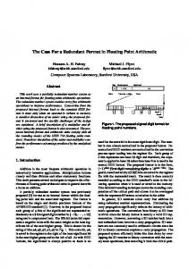
3. ROUNDING IN THE ADDER Fig. 1 shows the rounding logic used in the adder given our definition of the bits of the MSD and LSD. At the top left, simple logic gates use the bits of the MSD to determine the signals ld, lc, lb and la indicating the approximate leading bit. Once the signed sticky (ss) signal is known, the exact location is determined. The signed sticky is generated by another block that is not shown in this figure and it indicates whether the bits below the leading one of the MSD constitute a positive or negative number. Hence there are five possibilities for the exact location of the leading bit: either one of the four bits of the MSD or one bit lower than d. This last cases occurs if a = b = c = 0, d = 1 and ss = 1. Let us call this case dm as a short for d minus one. If the leading bit is a then the location of rounding is at bit f of the LSD and so on for the other locations. The primitive rounding logic block to the left of the figure is responsible for generating the speculative bits indicating the rounding value. The rounding value can be positive, negative or zero and hence is represented by two bits rp and rn and its value is given by rp − rn . Since the digits in the proposed format are always between −15 and +15, then the digit that was shifted out and from which the guard and round bits were drawn also falls in that range. Hence, if g1 = 1 we are guaranteed that at least one other bit in that digit that was shifted out is one. So, either g0 = 1, r = 1 or the sticky digit is positive (i.e. s1 = 0 and s0 = 1). This property insures that the fractional range at bit i the least significant bit of the LSD is bounded between −1 and 1. At g0 , this property insures that the fractional range is bounded between 0 and 1. For the other bit locations, the fractional range is bounded between −0.5 and 1. Given the location of the leading bit, the values of rp and rn are derived based on Table 1 resulting in the equations shown in Table 2. Those equations insure that either rp = rn = 0 or only one of them is set to one but never both at the same time. The Digit rnd part in the middle of the figure generates three possible outcomes for the cases of positive, zero or negative rounding value at each possible rounding location. These outcomes are the values of the bits in the locations of e to g0 which we can call e0 to g00 to signify the rounded values. In addition to that there might be a carry out (co) to the next higher digit. These values are given by the logic equations shown in Table 3. A few important points played a role in deriving those equations: 1. Since rp and rn are mutually exclusive, it is possible to use only one signal, co, to denote a positively valued carry in the case of rp = 1 and a negatively valued carry otherwise. 2. For the rest of the units, it is important to guarantee that the generated digits are between −15 and +15. Hence, even in the case of truncation of the LSD there might be a carry out of it. This occurs if e = 1 and the other bits that were to remain are all zeros. In this case, a co = 1 signal is generated and e0 is reset to zero. 3. The case of rounding at g0 is slightly different. rp = 1: Then g00 = g 0 , g10 = g1 g 0 and a carry of g 1 g0 must be added to the LSD. A multiplexer with g 1 g0 as a select line is used to choose between the outcome of rounding at i when the rounding value is 1 or 0. rp = rn = 0: This is a case of truncation and, as above, we must guarantee that the new digit is within the permissible range. Hence, g00 = g0 but g10 = g1 g0 and a negatively valued carry of g1 g 0 is added to the LSD. Again, a multiplexer with select line equal to g1 g 0 is used to choose between the rounded LSD at location i when the rounding value is −1 or 0. rn = 1: Then g00 = g 0 , g10 = g 0 and a negative carry of g1 is added to the LSD. The select line of the multiplexer is then g1 and the inputs are the rounded LSD at i when the rounding value is −1 or 0.
M=10
a a b c
g1 g0
ld 0 i h g
M=10
e e
f
lc
M=4 f
e
P:16
g
cb M=4
N:8 P:16
M=10 P:16
h
b
h
lb
ri0 rh0 rg0 rf0 re0 rc0 rip1 rc0 rhp1 rgp1 rfp1 rep1 rcp1 rim1 rcp1 rhm1 rgm1 rfm1 rem1 rcm1 rcm1
Digit rnd
bb
N:8
N:4
g0
f g h i g1 g0 r0 s1s0
0
rsg00 rsg0p1
rsg1p1 rsg1m1
rp
nrprnns rcm1
gnd rsc0 rc0
rp
rp
N:4 dmrn
crn brn drn
brp crpdrp
sign
M=4 nrprns
rns
rps rns
D
C
B
A
D
C
B
A
D
C
Out
ABCD Select
Out
ABCD Select
Out
ABCD Select
rns1 P:16
N:8
N:8
rps1 P:16
rnns1 P:16
N:8
N:8
ss
rpns1 P:16
ss
B
Out
rne
A
lb
ABCD Select
lc
D
ld
C
rne
B
rz
la
l[3:0]
rnns ss
sel1 sel2 sel3 in3 out in2 rcmns in1 Mux3to1 Mux3to1 rcms in1 in2 out in3 sel1 sel2 sel3
Sel_A B
rcm
Out A
rcm
rpns
Sel_A B Out
gnd
A
rcpns
rcp1 rscp1
sign rz
ln l[3:0]
nrprnsrps rns
out[4:0] Digit Mux
rm
P:16 rps
[3:0]
xn 1 digit muxon x[3:0] o[3:0] yn y[3:0] sel_y
rpns
in1[4:0]
rne
f g h i g10 r0 s10 rm rp primitive rounding logic sign rz rne a b c d dm pn pn pn pn pn dmrp arp arn
in2[4:0]
rz
in3[4:0] sel1 sel2 sel3
sign
rm
rpns rnns
gnd rscm1
0
rm
s0
s0
[3:0] ls[4:0]
rpns rnns rsg0m1
0
s1
s1
lns[4:0]
0
r0
Digit Muxout[4:0]
in3[4:0] sel1 sel2 sel3
rsg10
rsc0
r0
in2[4:0]
rscp1
rscm1
g0
in1[4:0]
N:4
g1 g1
ln
0
P:16
la
rsg00 rsg10 rsi0 rsh0 rsg0 rsf0 rse0 rsc0
i
rsg0p1 rsg1p1 rsip1 rshp1 rsgp1 rsfp1 rsep1 rscp1
rsg0m1 rsg1m1 rsim1 rshm1 rsgm1 rsfm1 rsem1 rscm1
i
A
Sel_A
rcps
A
rcmns ls[4:0]
B
rno_cpcmns
rcpns
A
Sel_A
N:4 P:16
rcp
B
gnd
rcp
Out
Out
P:16
Sel_A
rps
rno_cpcms
B
rno_cpcm
Out
rcps
A
rno_cpcm
N:4 rcms
P:8
N:4
P:8
N:4
P:8
N:4
P:8
N:4
Figure 1. Rounding of the least significant digit.
g
g1 g0
nrprnns M=3
ld lc lb la
f c
i h g f e ld lc lb la
rsg10 Mux3to1 rsg1p1 in1 out in2 in3 rg1s sel1 sel2 sel3 rsg1m1
A
rg1
Out B
gnd
rg1 Sel_A
M=5 rns
M=5 rps
M=5 rnns
M=5 rpns
nrprnsrps rns rsg00 Mux3to1 in1 rsg0p1 in2 out in3 rg0s sel1 sel2 sel3 rsg0m1 nrprnsrps rns
A
rg0
Out B
gnd
rg0 Sel_A
Table 2. Logic equations for rp and rn Leading bit
Rounding value
Round at
rp = dm
RNE rs1 (s0 + g0 )
g0
d
+ (RP sign + RM sign)(r + s1 s0 ) rn =
(RP sign + RM sign + RZ)rs1
rp =
RNE g 1 g0 rs1 (r + s0 + i) + (RP sign + RM sign)g 1 (g0 + r + s1 s0 )
i rn =
RNE g1 (g 0 + rs1 + r s0 i) + (RP sign + RM sign + RZ)(g1 + g 0 rs1 )
rp = c
RNE i(g1 + g 1 g 0 rs1 )(g0 + r + s0 + h)
h
b
+ (RP sign + RM sign)(i + (g1 + g 1 g 0 rs1 )(g0 + r + s0 )) rn =
(RP sign + RM sign + RZ)i(g1 + g 1 g 0 rs1 )
rp =
RNE h(i + (g1 + g 1 g 0 rs1 ))(i + g0 + r + s0 + g)
g
a
+ (RP sign + RM sign)(h + i + (g1 + g 1 g 0 rs1 )(g0 + r + s0 )) rn =
(RP sign + RM sign + RZ)hi(g1 + g 1 g 0 rs1 )
rp =
RNE g(h + i + (g1 + g 1 g 0 rs1 ))(h + i + g0 + r + s0 + f )
f
+ (RP sign + RM sign)(g + h + i + (g1 + g 1 g 0 rs1 )(g0 + r + s0 )) rn =
(RP sign + RM sign + RZ)ghi(g1 + g 1 g 0 rs1 )
Table 3. Logic equations for the rounded LSD Round at
co
e0
f0
g0
h0
i0
g10
g00
ef ghi
e(f ghi)
f ⊕ ghi
g ⊕ hi
h⊕i
i
0
0
0
e
f
g
h
i
0
0
−1
ef gh
ef ghi + e(f ghi)
f ⊕ (g + h + i)
g ⊕ (h + i)
h⊕i
i
0
0
+1
ef gh
e(f gh)
f ⊕ gh
g⊕h
h
0
0
0
0
ef gh
e(f + g + h)
f
g
h
0
0
0
−1
ef g
ef gh + e(f gh)
f ⊕ (g + h)
g⊕h
h
0
0
0
+1
ef g
e(f g)
f ⊕g
g
0
0
0
0
0
ef g
e(f + g)
f
g
0
0
0
0
−1
ef
ef g + e(f g)
f ⊕g
g
0
0
0
0
+1
ef
ef
f
0
0
0
0
0
0
ef
ef
f
0
0
0
0
0
−1
e
f
f
0
0
0
0
0
rp − rn +1
i
h
g
f
0
The logic deciding the ss signal detects the sign of each digit and whether it is zero or not. Then, a priority encoder (O(log n) operation) is used to determine the value of ss. Hence ss is a late signal and the Digit rnd block speculatively uses the approximate location of the leading bit to multiplex all the possible outcomes and to generate two sets of digits. A set for the case of a zero signed sticky and another set for the case of a signed sticky equal to one. As shown in Fig. 1, the set assuming that the signed sticky is one enters into the multiplexer in the center of the figure that selects the correct digit depending on the values of rp and rn given that ss = 1. The other set is channeled to the multiplexer to the right of the Digit rnd block which also selects the correct digit depending on the values of rp and rn given that ss = 0. Finally, the multiplexer to the top right of the figure gives the final output digit depending on the value of ss. The signed sticky ss is also used as a select line for the other multiplexers to the right of the figure giving the values of the rounded g1 and g0 as well as the possible three values for the carry out to the next higher digit: rcp = 1 if it is positive, rcm = 1 if it is negative otherwise if it is zero the signal rno-cpcm is set to one.
4. ROUNDING IN THE MULTIPLIER A subtle difference between the multiplier in the proposed system and the conventional multipliers is the fact that each operand has a number of bits that are considered to have a negative value. These are the extra bits in each digit of the number. The significands of the two operands X and Y are thus assumed to have three components: P the positively valued bits, E the negatively valued extra bits and r the value of the rounding digit which is either positive or negative (i.e. r ∈ {−1, 0, 1} .) The end result is X × Y but, X = Px − Ex + rx and Y = Py − Ey + ry and hence a number of possibilities for the design were studied.9 Similar to the case of the floating point adder, rounding in the presented floating point multiplier proved to be a challenge. The operands can be rounded first and then the rounded significands used to perform the multiplication. This puts the rounding logic on the critical path of the multiplier and delays the start of the partial products reduction. Rounding first without any other parallel work done on the significands is unacceptable if a high speed multiplier is required. It adds a time delay comparable to the time needed for the partial product reduction tree using [4 : 2] compressors.9 Another possibility is to chop both operands X and Y at the rounding location. Then, simultaneously, some additional partial products with the values ry (Px − Ex ), rx (Py − Ey ) and rx ry are generated. In this second case, the reduction of the partial products starts directly but it takes more hardware because of the added partial products. As mentioned in the discussion on rounding in section 2, this rounding location is determined by the leading bit of the MSD and the signed sticky digit. The operand chopping takes away all the bits below the approximate rounding location determined only by the leading bit of the MSD. The multiplication is carried as (Xchopped + (bx + rx ))(Ych + (by + ry )) where bx and by are the bits directly after the rounding location in case the signed sticky indicates a negative fractional value while rx and ry are the rounding digits. Hence the multiplication can be divided into three parts: X × Y = Xchopped Ychopped +(bx + rx )Ychopped + (by + ry )Xchopped +(bx + rx )(by + ry )
By Booth recoding, generating partial products and summing 2 special partial products added in the tree special correction added to the tree
Fig. 2 shows how (by + ry )Xchopped is formed.∗ The rounding portion (by + ry ) is done by feeding the bits of Y to the correction block in the bottom right of the figure to generate five shifting signals sh4 to sh0 and the correction rounding value. The output of the correction rounding value or is coded by two bits orp and orn and its value is orp − orn . In the figure, the complement of those two signals are shown as orpb and ornb. This correction block at the bottom right basically recodes the multiplication by (by + ry ) as a multiplication by 2shif t followed by a selection of either the positive or negative of the shifted operand based on the value of the orp and orn signals. ∗
Obviously, the same circuit with the inputs reversed can do (bx + rx )Ychopped .
op[64] A
ip[59] gnd
gnd
D
op[64:3]
Select E ABCD E
pospp[64:3]
A A
op[62]
B
on[64:3]
Out C
pospp[64:3]
Out
Mux2 def0 B 62b Select Ab Bb
D Select E ABCD E
gnd gnd
in[14:0]
gnd
Out C
gnd gnd gnd ip[58] ip[59]
ip[59:3]
op[63]
B
A
ip[57] ip[58] ip[59] gnd gnd ip[56] ip[57] ip[58] ip[59] gnd ip[55] ip[56] ip[57] ip[58] ip[59] in1[3:0] in2[3:0] in3[3:0] in4[3:0] in5[3:0]
ip[54:51] ip[55:52] ip[56:53] ip[57:54] ip[58:55]
op[61]
B
op[64:3]
D Select E ABCD E A B
Mux2 def0 B 62b
op[59]
orpb ornb
D Select E ABCD E A B Out C
Mux n 61b
D Select E ABCD E
ni
on[64:4]
o[63:3]
in[14:0] op[58:55]
on[3]
a b c d dm
Mux5_4b
gnd
out[3:0]
sel1 sel2 sel3 sel4 sel5
in1[15:0] in2[15:0]
op[38:23]
in1[15:0] in2[15:0] in3[15:0] in4[15:0] in5[15:0]
op[22:7]
in3[15:0] Mux5_16b out[15:0] ip[34:19] in4[15:0] ip[35:20] in5[15:0] ip[36:21] sel1 sel2 sel3 sel4 sel5 ip[37:22] ip[38:23]
sh4
sh0
sh1 sh3 sh2 sh2
out[15:0] Mux5_16b sel1 sel2 sel3 sel4 sel5
sh3 sh1 sh4 orpb sh0 ornb
Out C
i2ns0 i2ps[7:0] sign r[3:0] ld lc lb la ss
D Select E ABCD E A
corr_sh_r
op[6]
B
ornb orpb
sh0 sh1 sh2 sh3 sh4
A
gnd gnd
Select Ab Bb
Out C
op[54:39]
ip[3] ip[4] ip[5] ip[6]
Out
op[60]
in1[15:0] in2[15:0]
gnd
negpp[64:3]
A
on[64:3]
in3[15:0] Mux5_16b out[15:0] ip[50:35] in4[15:0] ip[51:36] in5[15:0] ip[52:37] sel1 sel2 sel3 sel4 sel5 ip[53:38] ip[54:39]
ip[18:3] ip[19:4] ip[20:5] ip[21:6] ip[22:7]
ornb orpb
Out C
op[5]
B Out C
gnd gnd gnd
D Select E ABCD E A
op[4]
B
i2ns0 i2ps[7:0] sign r[3:0] ld lc lb la ss
ip[3] ip[4] ip[5]
Out C D
ip[3] ip[4] gnd gnd gnd gnd
Select E ABCD E A
op[3]
B Out C D Select E ABCD E
ip[3] sh4
sh0
sh1 sh3 sh2
Figure 2. Multiplying one operand by the rounding part of the other.
negpp[64:3]
The correction block must decide on the exact amount of shifting to be done. For this to be achieved, the leading one of the MSD of Y is detected. Similar to the rounding in the adder, let us assume that the bits of the MSD are a b c d and let us assume that the signals indicating which bit is the leading one are labeled la, lb, lc and ld. Those signals are among the inputs to the correction block. The other inputs are the value of the signed sticky ss, the rounding mode selectors, the sign of the operand and the bits of the LSD and guard, round and sticky digits of Y . As in the discussion of the adder, let us define the bits of Y as: a b c
d ···
···
··· f e
g
h
i g0 g1
r s1
s0
If the signed sticky is not set (ss = 0), the value of by the bit directly after the rounding location is irrelevant, the output corrected value or is given by ry alone and the shifting amount is determined only by the leading one of the MSD. On the other hand, if ss = 1 then by must be considered. The evaluation of (by + ry ) is tricky since ry can be negative, zero or positive while by is positive or zero except at the g0 location where it might be negative, zero or positive. Hence, when ss = 1 and the rounding is not at the g0 location: If both by and ry are positive then (by + ry ) = 2 which means that, effectively, it is carried to the next higher bit location and the shift amount is increased by one canceling the effect of ss. Otherwise, the effect of ss is taken into account and the shift amount derived based on it. at the g0 location: The value of g1 g0 is given by −2g1 + g0 and can be in {−2, −1, 0, 1} • g1 g0 = 01 = (1) then, as above, if ry = 1 it is a carry to the next higher bit. Otherwise, the effect of ss is taken into account. • g1 g0 = 00 = (0) then by = 0 and the effect of ss is taken into account. • g1 g0 = 11 = (−1) then if ry = −1 (note the sign) it is a carry to the next higher bit. Otherwise, the effect of ss is taken into account. • g1 g0 = 10 = (−2) in this case ry ∈ {0, 1}† and if it is zero a carry to the next higher bit occurs. Otherwise, the effect of ss is taken into account. Since the rounding location could be anywhere from the g0 location to the f location, the shift amount produced by the correction block is assumed to be zero if the value of (by + ry ) evaluates to be at the g0 location. Let the rounding values at any location be represented by rp and rn with a subscript referring to the leading bit of the MSD corresponding to this location. These rounding values are evaluated by the primitive rounding logic block described in the discussion of Fig. 1. The signals for the shift are then given by the following equations: sh4
= ss la + ss la(grpb )
sh3
= ss lb + ss la(grpb ) + ss lb(hrpc )
sh2
= ss lc + ss lb(hrpc ) + ss lc(irpd )
sh1
= ss ld + ss lc(irpd ) + ss ld(g 1 g0 rpdm + g1 g0 rndm + g1 g 0 rpdm )
sh0
= ss ld (g 1 g0 rpdm + g1 g0 rndm + g1 g 0 rpdm )
The output corrected rounding value or corresponds to the value of by + ry regardless of the shift. So, or = 0 if by + ry = 0, or = 1 if by + ry = 1 or 2 and or = −1 if by + ry = −1 or −2. To calculate orp and orn , we can use two intermediary signals rp and rn indicating the value of ry , rp rn †
= ss(la rpa + lb rpb + lc rpc + ld rpd ) + ss(la rpb + lb rpc + lc rpd + ld rpdm ) = ss(la rna + lb rnb + lc rnc + ld rnd ) + ss(la rnb + lb rnc + lc rnd + ld rndm )
Due to the condition on the number system that a digit cannot be −16, if g1 g0 = 10 then in the bits representing the guard round and sticky digits either the round bit r = 1 or the sticky digit is positive. This leads to only a positive fractional value at g0 which means that the rounding value at this location cannot be negative as noted in section 3.
The signals for orp and orn are mutually exclusive to fit their role as multiplexer select signals in Fig. 2. The signal orp is set to 1 if ry = 1 and by is neglected in the case of ss = 0 or by = 0. The other case where orp is set is if ry is not a negative one and by = 1. In boolean logic this translates to: orp = ss rp + ss rp (la g + lb h + lc i + ld g 1 g 0 ) + ss rn (la g + lb h + lc i + ld g 1 g0 ) Similarly, orn is set to 1 if ry = −1 and by is neglected in the case of ss = 0 or by = 0. The second case where orn is set is if ry is not a positive one and by = −1 (g1 g0 = 11) or by = −2 (g1 g0 = 10). The third case is if ry = 1 and by = −2. In boolean logic this translates to: orn = ss rn + ss rn (la g + lb h + lc i + ld g 1 g 0 ) + ss rp ld g1 + ss rp ld g1 g 0 With the values of sh4 to sh0 , orp and orn the multiplexers of Fig. 2 shift and choose the correct positive and negative outputs as seen in the top left part of the figure. The calculation of the special correction (bx + rx )(by + ry ) is done in a similar fashion. The same correction block described above is used for both operands X and Y . A few logic gates determine that the result is positive if the output corrected rounding values of both X and Y are of the same sign. The result is negative if those values are of opposite sign. The special correction is represented redundantly by a positive and a negative bit vector where the correct bit location is set depending on the output corrected rounding values and the sign of the result.
5. CONCLUSIONS Due to the redundancy, the rounding location may shift by one bit depending on the signed sticky of the part below the leading bit of the number being rounded. Since the generation of this signed sticky depends on all the bits of the number, it is slow. In the adder, a special attention is given to optimize the speed of the hardware given the slow signed sticky by speculatively calculating different possibilities for the rounded LSD. Once the exact rounding location is determined the corresponding rounded LSD is chosen. For the multiplier, the generation of the rounding correction is explained and an efficient implementation is presented. For both the adder and the multiplier the rounding hardware has been relocated to have its time delay masked by another essential operation. This masking takes the rounding delay off the critical path of the units.
REFERENCES 1. P. M. Farmwald, On the Design of High Performance Digital Arithmetic Units. PhD thesis, Stanford University, Aug. 1981. 2. N. T. Quach, Reducing the latency of floating-point arithmetic operations. PhD thesis, Stanford University, Dec. 1993. 3. A. Beaumont-Smith, N. Burgess, S. Lefrere, and C. C. Lim, “Reduced latency IEEE floating-point standard adder architectures,” in Proceedings of the 14th IEEE Sympsoium on Computer Arithmetic, Adelaide, Australia, pp. 35–42, Apr. 1999. 4. P.-M. Seidel and G. Even, “On the design of fast IEEE floating-point adders,” in Proceedings of the 15th IEEE Sympsoium on Computer Arithmetic, Vail, Colorado, USA, pp. 184–194, July 2001. 5. H. A. H. Fahmy, A. A. Liddicoat, and M. J. Flynn, “Parametric time delay modeling for floating point units,” in The International Symposium on Optical Science and Technology, SPIE’s 47th annual meeting (Arithmetic session), Seattle, Washington, USA, July 2002. 6. M. R. Santoro, G. Bewick, and M. A. Horowitz, “Rounding algorithms for IEEE multipliers,” in Proceedings of the 9th IEEE Sympsoium on Computer Arithmetic, Santa Monica, California, USA, pp. 176–183, Sept. 1989. 7. M. I. Furgeson and M. D. Ercegovac, “The IEEE rounding for multiplier with redundant operands,” in Thirty-Fourth Asilomar Conference on Signals, Systems, and Computers, Asilomar, California, USA, 2, pp. 1334–1338, Oct. 2000. 8. H. A. H. Fahmy and M. J. Flynn, “The case for a redundant format in floating point arithmetic,” in Proceedings of the 16th IEEE Sympsoium on Computer Arithmetic, Santiago de Compostela, Spain, June 2003. 9. H. A. H. Fahmy, A Redundant Digit Floating Point System. PhD thesis, Stanford University, June 2003.