the use of so-called tapered interdigital transducers. (TIDT) as first introduced over more than 25 years ago by Van de Heuvel [5]. A detailed discussion of.
IEEE ULTRASONICS SYMPOSIUM 1999, LAKE TAHOE, USA
1
SAW Tomography - Spatially Resolved Charge Detection by SAW in Semiconductor Structures for Imaging Applications M. Streibl1, F. Beil1, A. Wixforth1 , C. Kadow2 and A.C. Gossard2 1
CeNS and Sektion Physik der LMU M¨ unchen, Geschw.-Scholl-Pl. 1 , D-80539 Munich, Germany 2
Materials Department and QUEST, University of California, Santa Barbara, California 93106
Abstract— The interaction of surface acoustic waves and free carriers in a nearby semiconducting sheet yields an extremely sensitive method for sensing electrical and optical signals. In the present work we demonstrate the spatially resolved detection of optical signals with a spatial resolution of a few acoustic wavelengths. We exploit the high selectivity of socalled tapered transducers to excite adjustable narrow acoustic beams allowing for the scanning of photogenerated charge distributions. Using a special layout, both x and y- coordinate of the optical signal are readily read out in a single frequency sweep. Complex 2D image information can be gathered when a tomographic imaging technique is applied. I. SAW and Semiconductor Systems The combination of advanced state-of-the-art SAW device technology with the superior electronic properties of a semiconductor structure in either a monolithic or hybrid approach paves the way to a whole range of interesting signal processing applications. The interaction of a surface acoustic wave with free carriers in a nearby semiconducting sheet allows for a tunable attenuation and phase shift of the SAW signal. The coupling of the acoustic wave to an electron system in the semiconductor is mediated by the piezoelectric fields accompanying the SAW and is summa2 rized in the electromechanical coupling constant Keff . In general, for a conducting sheet close to the surface having a conductivity σ the change in velocity is given by [1] 2 Keff ∆v 1 = v 2 1 + (σ/σm )2
(1)
where σm denotes a crititical conductivity where the energy transfer from the SAW to the electron system is largest, i.e. induced screening currents are dissipative. The energy loss by screening currents leads
to an attenuation of the acoustic waves which is characterized by Γ=
σ/σm Keff kSAW 2 1 + (σ/σm )2
(2)
For hybrid systems, where strong piezoelectric substrates like LiNbO3 are combined with a semiconducting sheet of submicron thickness, phase shifts of several hundred degrees and attenuations of about −20db have been demonstrated [2]. The coupling of SAWs and an electron system hence provides a simple and extremely sensitive method for the determination of the semiconductors properities and provides a versatile mechanism for a whole range of electrical and optical sensing applications. Because of its high sensitivity it has been extensively used in the last decade in fundamental reserach. SAW based experiments contributed significantly to the investigation of two-dimensional electron system in the quantum hall regime [3] and in the fractional quantum hall regime [4]. II. Tapered IDTs for Spatial Resolution In the present work, we demonstrate the spatially resolved imaging of optical signals in one and two dimensions with a spatial resolution of a few acoustic wavelengths. The spatial resolution is achieved by the use of so-called tapered interdigital transducers (TIDT) as first introduced over more than 25 years ago by Van de Heuvel [5]. A detailed discussion of its properties and applications is given for example by Solie et al. in [6]. The basic operation of the tapered transducer is shown in Fig. 1. The finger period p(y) is increased monotonically along the transducers aperture L. This results on the one hand in a spread of the transducers resonance into a bandpass determined by the degree of tapering. On the other hand, for a given frequency f in the bandpass a narrow SAW beam is launched exclusively where the resonance condition p(y) · f = vSAW is matched. It is mainly the spread of the IDT’s bandpass which yields applications in wide band delay lines and bandpass filters. The width
IEEE ULTRASONICS SYMPOSIUM 1999, LAKE TAHOE, USA
w =L·
∆f 0.9 =L . ∆ftap tN
(3)
Our TIDTs were fabricated by electron beam lithography and had center frequencies between 570MHz and 1.5 GHz, meaning transducer periods from 5µm down to 2µm. The effective aperture was L = 400µm, the number of fingerpairs N = 100. Lithographic limitations resulting from the large transducer aperture forbid a split electrode layout. In fact, internal acoustic reflections in the single electrode structure used enhances the transducers selectivity and reduces ∆f by about a factor of 4. For typical taper factors t = 5%..10% we calculate from Eq. (3) a width of the acoustic beam between 10 to 20 µm. As this lengths are of the order of the acoustic wavelength diffraction effects are to be expected. In fact, we find a 10dB decrease of the SAW transmission when the taper factor t is increased from 5% to 10% as shown in Fig. 1 which clearly stresses the importance of diffraction. To check the intuitive picture given here, X-ray topography experiments were performed on our TIDTs by Sauer et al. [7]. The high resolution bragg reflection images with a spatial resolution of about 0.5µm taken at the ESRF in Grenoble clearly show the decrease of the width of the tapered SAW beam and the increase of diffraction effects when t is switched from 5% to 10%. However, as the second receiving transducer has the same selectivity, only the undisturbed components of the wave are detected keeping the spatial resolution unaffacted from diffraction effects. III. Spatial and Temporal Resolution As a first and simple test of the perfomance in sensing optical signals, a laser beam (λ = 860nm,
t=5% 28MHz
transmission [dB]
-40 -50 -60 -70
f1
f2
f3
t=10% 62MHz
f1
f2
f3
x
-80 -90 560
610 660 frequency [MHz]
y
L
0
Fig. 1. A SAW delay line featuring TIDTs. Because of the variation of the transducer period along its aperture, the SAW transmission is spread into a bandpass. A single frequency within the bandpass corresponds to a single narrow SAW beam launched at the respective position in the TIDT.
-6 rel. phase shift [deg]
of the bandpass can be estimated by ∆ftap = t · f0 p(L)−p(0) where the factor t = is introduced to inp(L) dicate the degree of tapering and f0 denotes the center frequency. Our experiments were performed both on bulk GaAs and on InGaAs/AlGaAs/GaAsheterostructures. GaAs is weakly piezoelectric with a 2 coupling constant of Keff = 6.4·10−4 which, however, 2 = 1.1 · 10−3 ). is comparable to ST-cut quartz (Keff To achieve reasonable SAW intensities, a large number N of finger pairs has to be used. For conventional IDTs, this results in a extremely narrow transmission, which is approximately given by ∆f = 0.9f0 /N . In the case of tapered IDTs, the extremely high selectivity in frequency for a large number of finger periods N translates into an extremely narrow acoustic beam. Its width can be estimated by
2
-4 -2 0 2 720
730 740 750 760 frequency [MHz]
Fig. 2. Phaseshift signal induced by a photogenerated electron hole plasma within the SAW path. The different traces correspond to different positions of the laser spot on the sample.
P = 150µW was focussed onto the acoustic path to create an electron hole plasma underneath. The resulting phaseshift of the SAW signal vs. frequency is shown in Fig. 2 for different positions of the laserspot. The gaussian shape of the electron hole plasma is well resolved as the phase shift is largest when the narrow acoustic beam launched at the TIDT hits the core of the charge distribution. Additionally to the spatial resolution, a temporal resolution of about 0.1µs is provided when the transmitted SAW signal is recorded in the time domain. For this modified experiment a diode laser was used to generate light pulses of 1µs lenght and an intensity of P = 30µW . The SAW attenuation is analyzed vs. frequency and time and depicted in Fig. 3. The asymmetric rise and decay of the gaussian charge distribution refers to µs lifetimes of photogenerated carriers in bulk GaAs. In a modified setup,
3
-60 -80
0 800
820
840
860
880
900
920
[a.u.]
-100
attenuation
transmission [dB]
attenuation [a.u.]
IEEE ULTRASONICS SYMPOSIUM 1999, LAKE TAHOE, USA
f requency [MHz]
space [µm]
5 400
time[µs] 0
Fig. 3. Spatially and time resolved detection of the rise and decay of the carrier plasma induced by a short laser pulse.
where the laser spot region was exposed to an additional high amplitude SAW beam the TIDT scanning of the carrier system clearly showed the appearance of a ’comet’s tail’ of acoustically transported carriers. However, these experiments are beyond the scope of this paper and will be presented elsewhere [8]. IV. Resolution in 2D When two orthogonal delay lines are combined in a cross shaped structure as shown in the inset in Fig. 4, both the x and y coordinate of an optical signal can be determined in the 400 × 400µm2 large square defined by the intersection of the two delay lines. For convenience the signals of the two acoustic paths have been merged by linking the horizontal and vertical source IDT and as well the two receiving IDTs to a single input and output as shown in the inset in Fig. 4. To distinguish between the two coordinates the 40M Hz passbands of the two delay lines have been offset to each other to 825M Hz and 895M Hz respectively. Hence one single frequency sweep provides the full spatial information. Fig. 4 shows the two passbands, the attenuation induced by a laserspot as recorded by a network-analyzer, and the reconstructed picture of the laserspot at verious positions. Not only can we detect the position of the laserspot with high spatial and temporal resolution, also its intensity and diameter can be measured, which is expressed by different spotsizes in the lower panel. V. SAW Tomography Scanning more complex images using the above cross geometry, ambiguities occur resulting from the fact that the interaction between scanning SAW beam
y x
Fig. 4. The intersection of two tapered delay lines defines a square within which the position of an optical signal can be detected with µm resolution. The inset schematically depicts the sample layout. The viewgraph shows the samples linked passbands and the attenuation induced by a moving laserspot as onedimensional traces or as twodimensional images in the lower panel.
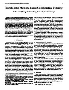
and photogenerated charges is integrated along the acoustic path. Mere superposition of the orthogonal SAW beams does not allow to adress a single pixel. This problem can in principle be overcome when a tomographic technique is applied as it is used in the x-ray absorption tomography of solid objects [9]. Here, the object is rotated with respect to the x-ray source, the projection from various angles is recorded and used to reconstruct the 2D or 3D structure of the object. In our case, we reproduce this technique by projecting an picture onto the acoustic path and scanning the induced charge distribution by the scanning SAW beam. The picture is then rotated by an arbitrary angle and the scanning procedure is repeated. Finally, we recorded a set of 1D intensity projections of the picture for various angles and then reconstructed the 2D image employing the procedure explained in Fig. 5a. To demonstrate the principle, the image of an double slit aperture was chosen and rotated in the acoustic path. Some projections recorded by frequency sweeps for angles between 0o and 180o are shown in Fig 5b. The picture reconstruction by back projection is schematically shown in Fig. 5c. The measured intensity profiles are equally distributed along the acoustic paths and added up. Usually, to enhance the edges and to correct the overestimation of the image center, where all backprojections overlap, the data are filtered in Fourier space by the filter function y(f) → y(f) · f. Following this procedure, we end up with the reconstructed image in Fig 5d. The spatial resolution is given on the one hand by the width of the scanning acoustic path and on
IEEE ULTRASONICS SYMPOSIUM 1999, LAKE TAHOE, USA
b) attenuation [a.u.]
a)
4
been used to excite narrow acoustic beams and to acoustically scan photogenerated charge distributions in a semiconducting system. 1D and 2D position information is given as attenuation or phaseshift signal within the transducers bandpass. Employing tomographic techniques as used in X-ray tomography, complex 2D images can be scanned and reconstructed.
1 0,8 0,6 0,4 0,2 0 725
c)
735 745 755 frequency [MHz]
765
d)
e)
VII. Acknowledgement The authors gratefully acknowledge enlightening discussions with J.P Kotthaus, A. Haubrich, and M. Rotter, technical advice from S. Manus and generous financial support of the Deutsche Forschungsgemeinschaft (DFG, SFB348) and the Bayerische Forschungsstiftung FOROPTO. The work at UCSB has been supported through AFOSR (grant No F49620-94-1-0158) and the center for quantized electronic structures (QUEST). References
Fig. 5. a) Principle of SAW tomography for scanning 2D image information; b) Acoustic scans from various angles; c) Picture reconstruction algorithm; d) Reconstructed image of a double slit aperture; e) Sample images of complex structures
the other hand by thermal carrier diffusion on a micrometer length scale which tends to blur out the picture. The original structure however is well resolved. To demonstrate that the SAW tomography approach also works for even more complex pictures we tried to scan images of the characters ’S’, ’A’ and ’W’. A collection of the resulting images is shown in Fig. 5e. With additional edge-enhancement not only the contour of the letter ’A’ but also its inner structure can be resolved as shown to the right. Future work will be concentrated on the improvement of the tapered delay lines and the enhancement of the sensitivity by employing hybrid systems as mentioned above. Further potential applications might result from the fact, that in configurations like presented in Fig. 4 the simultaneous detection of mechanical signals is easely achieved as the system can be operated as a micro-touchscreen. VI. Conclusions To conclude, we demonstrated the spatially resolved detection of optical signals with a resolution of a few acoustic wavelengths. Tapered transducers with center frequencies between 500MHz and 1.5GHz have
[1] A. Wixforth, J.P. Kotthaus and G. Weimann, Phys. Rev. Lett 56, 2104 (1986) [2] M. Rotter, A.V. Kalameitsev, A.O. Govorov, W. Ruile and A. Wixforth, Phys. Rev. Lett. 82, 2171 (1999) [3] A. Wixforth, J. Scriba, M. Wassermeier, J.P. Kotthaus, G. Weimann and W. Schlapp, Phys. Rev. B 40, 7874 (1989) [4] R.L. Willet, R.R. Ruel, W. West and L.N. Pfeiffer, Phys. Rev. Lett. 71, 3846 (1993) [5] A.P. Van de Heuvel, “Use of rotated electrodes for amplitude weighting in interdigital surface wave transducers”, Appl. Phys. Lett. 21, 280 (1972) [6] L. P. Solie, “A new low-loss, single-bounce, reflective array filter using hyperbolically tapered transducers with curved fingers”, IEEE Ultrason. Symp., 1986, pp.77-80 ; L. Solie, “Tapered Transducers - Design and Applications”, IEEE Ultrason. Symp. 1998. [7] W. Sauer, M. Streibl, T. H. Metzger, A. G. C. Haubrich, S. Manus, A. Wixforth, J. Peisl, A. Mazuelas, J. H¨ artwig, and J. Baruchel, Appl. Phys. Lett. 75, 1709-1711 (1999); W. Sauer et al., “Imaging Surface Acoustic Waves on GaAs by X-Ray Diffraction Techniques”, to be presented at IEEE Ultrason. Symp. 1999 [8] M. Streibl at. al., Appl. Phys. Lett., in press [9] J. C. Russ, “The Image Processing Handbook”, Second Edition. Boca Raton, FL:CRC Press, 674 pp. (1995)