SCIMA: Software Controlled Integrated Memory Architecture for High Performance Computing Hideki OKAWARA1 Research Center for Advanced Science and Technology, The University of Tokyo
[email protected]
Masaaki KONDO Research Center for Advanced Science and Technology, The University of Tokyo
[email protected] Hiroshi NAKAMURA Research Center for Advanced Science and Technology, The University of Tokyo
[email protected]
Taisuke BOKU Institute of Information Sciences and Electronics, University of Tsukuba
[email protected]
Abstract
Even if temporal locality is available to some extent, cache is not the best mechanism to exploit the locality. First, data which will not be used again pollutes the cache and flushes out other data which will be used soon. Second, line conflicts flush out useful data unfortunately from the cache. The essential reason for these problems is that it is by far difficult for hardware to control data location and data replacement. Because most of the data accesses in HPC (High Performance Computing) applications are regular, better performance can be obtained by software control of data location and replacement. Thus, we propose a new VLSI architecture named SCIMA: Software Controlled Integrated Memory Architecture. SCIMA integrates software-controllable addressable memory into processor chip as a part of main memory in addition to ordinary cache. Hereafter, we call that memory “OnChip Memory” (As opposed to that, we call off-chip main memory “Off-Chip Memory”). Since On-Chip Memory is explicitly addressed by software, only the required data is pre-transferred into the On-Chip Memory without flushing out other required data. Unfortunate conflicts will not occur. In this point, On-Chip Memory is better to exploit temporal locality than cache. Therefore, SCIMA has the potential to solve the problems of cache and achieve higher performance. We have already described basic concept of SCIMA in [3]. In this paper, we newly present the advanced mechanism where On-Chip Memory and cache share the hardware memory structure varying the utilization ratio on it. We also present a detailed performance evaluation and analysis of that mechanism by using real HPC application.
Processor performance has been improved due to clock acceleration and ILP extraction techniques. Performance of main memory, however, has not been improved so much. The performance gap between processor and memory will be growing further in the future. This is very serious problem in high performance computing because effective performance is limited by memory ability in most cases. In order to overcome this problem, we propose a new VLSI architecture called SCIMA which integrates software controllable memory into a processor chip. Most of data access is regular in high performance computing. The software controllable memory is more suitable for making good use of the regularity than conventional cache. This paper presents its architecture and performance evaluation. The evaluation results reveal the superiority of SCIMA compared with conventional cache-based architecture.
1. Introduction Processor performance has been improved drastically by clock acceleration and ILP (instruction-level parallelism) extraction technique. Main memory performance, however, has not been improved so much. This performance disparity between memory and processor is serious problem, which is called memory wall problem[1]. In order to solve this problem, cache memory is widely used. However, cache is not effective in large scientific/engineering applications[2]. Because data set is much larger than cache capacity and temporal locality cannot be fully exploited, cache miss occurs frequently and performance is degraded seriously. 1 Currently
Related works. There have been many studies on integrating DRAM and processor into a single chip.
with FUJITSU LABORATORIES LTD.
1
ALU
FPU
register
Cache
Processor Chip 0x000..0
MMU
a
On-Chip SRAM b1 b2 : bn
ASR b1
AMR 11....1100.....00
On-Chip Memory B1 B2 : Bn
TLB
A
NIA Memory (DRAM)
0xfff..f logical address space
Network
physical Memory (Off-Chip)
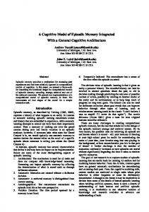
Figure 1. Overview of SCIMA
Figure 2. Address space
IRAM[4] implements a vector processor on a DRAM chip in order to exploit the high memory bandwidth within a chip. PPRAM[5] also aims at high performance by using integrated DRAM memory of high bandwidth and low latency. However, their studies assume that the required data set fit into the on-chip memory. They do not pay much attention how to supply data from off-chip memory. The target of our study is HPC applications whose data set is too large to be fitted in on-chip memory even if DRAM is used. Thus, we focus on how to improve the performance of the whole memory system including on-chip and off-chip memory. At this point, our work is different from IRAM or PPRAM. There have been proposed some processors which adopt small scratch pad RAM [6][7]. However, those scratch pad RAMs are used for specific applications. On the other hand, the target of SCIMA is wide area of HPC applications. Compiler-Controlled Memory[8] is a small on-chip memory which is controlled by compiler. However, this memory is used for only spill code. On-Chip Memory of SCIMA, on the other hand, can be used for all the data if required. The target of SCIMA is wide area of HPC applications which have large data set. SCIMA realizes flexible and explicit (or software-controllable) data transfer between on-chip and off-chip memory. This is the main difference between our SCIMA and other works.
if DRAM is used. We put higher priority in the fast access time rather than large capacity. The main difference between On-Chip Memory and cache is that the location and the replacement of data are controlled by software explicitly in On-Chip Memory, whereas those of cache are controlled by hardware implicitly. Cache is still provided to work for irregular data accesses.
2. SCIMA
On-Chip Address Start Register (ASR) This register holds the beginning logical address of On-Chip Memory: This address must be aligned to the multiple of On-Chip Memory size.
2.2. Address space Locations in the On-Chip Memory should be explicitly identified by software because its throughput and latency are different from those of Off-Chip Memory and these differences should be fully taken into consideration for performance optimization. In SCIMA, OnChip Memory occupies one consecutive part of logical address space. Because we assume On-Chip Memory is much larger than ordinary page size, frequent TLB misses occur and the performance is greatly degraded if On-Chip Memory is controlled by ordinary TLB. Therefore, On-Chip Memory is treated as a large page. Two special registers are introduced to identify the On-Chip Memory area as shown in Figure 2. On-Chip Address Mask Register (AMR) This mask register indicates the size of On-Chip Memory: If the least significant m bits of AMR are 0, On-Chip Memory size is 2m byte.
2.1. Overview Figure 1 shows the schematic view of the proposed architecture SCIMA. In SCIMA, addressable On-Chip Memory is integrated into the processor chip in addition to ordinary cache. We employ SRAM as the OnChip Memory. Since our target is HPC applications, the whole data cannot reside in On-Chip memory even
Since the address check for On-Chip Memory is quite simple by using the two registers, it can be performed in very short time. Inclusion relation between On-Chip Memory and cache. All the address space has a 2
cacheable/uncacheable property. This property is managed by TLB and page-table mechanisms like the ordinary current processors. In SCIMA, the On-Chip Memory space, which is not under control of TLB, is always handled as uncacheable. Therefore, there is no inclusion relation between On-Chip Memory and cache.
total cache size ASR
Way3
Way2
Way1
Way0
x... x 0 0 0 ........0
AMR 1... 1 1 0 0 ........0 SET LINE WAY WAY SIZE
Data transfer among memory hierarchy. If a memory access is for the On-Chip Memory, the access goes only to On-Chip Memory. Otherwise, the access goes to cache or Off-Chip Memory. If the accessed address is within cacheable area, the access goes to cache at first. If cache does not hit, then the access goes to Off-Chip Memory. If the address is within uncacheable area, the access goes directly to Off-Chip Memory. Thus, the following three kinds of data accesses are available in total.
log(4)
OMV 1
log(8k)
WLR 0 0 1 1 3210
Cache
On-Chip Memory
Figure 3. Unification of On-Chip Memory and cache
Hardware structure. In addition to ASR and AMR described in section 2.2, we introduce the following special registers for unifying On-Chip Memory and cache.
• register ↔ On-Chip Memory ↔ Off-Chip Memory • register ↔ cache ↔ Off-Chip Memory
Way Lock Register (WLR) The bit width of this register is equal to the degree of cache associativity (the number of ways): If the bit of the corresponding way is set to on, that way is locked as On-Chip Memory.
• register ↔ Off-Chip Memory 2.3. New instructions In order to control data transfer between On-Chip Memory and Off-Chip Memory, special instructions, page-load and page-store, are newly introduced. These instructions can specify block-stride data transfer. Using this feature, non-consecutive data on Off-Chip Memory can be packed and transferred into a consecutive area on On-Chip Memory. This ability allows effective utilization of On-Chip Memory. Notice that the term page employed in these instructions is different from ordinary page utilized for virtual addressing. This page indicates the unit of On-Chip Memory management. Hereafter, the term page refers this management unit through this paper without any attention.
On-chip Memory Valid(OMV) This register has 1 bit entry which indicates whether any way is utilized as On-Chip Memory. Figure 3 shows the hardware structure. This Figure illustrates the case where 32KB 4way cache is divided into 16KB 2way cache and 16 KB On-Chip Memory. Allotment of On-Chip area is dynamically executed by a system call. When the system call is executed, data in the corresponding ways is flushed out, the corresponding bits of the WLR and OMV are set to on, and appropriate values are set to AMR and ASR. The WAY bits of AMR indicate the number of ways locked as On-Chip Memory and the WAY bits of ASR indicate the way from which On-Chip Memory is allocated. In Figure 3, the WAY bits of AMR are 10 and that of ASR are 00. This indicates that two ways are utilized as OnChip Memory and locked beginning from way 0. Table 1 shows the possible allotments of On-Chip Memory in the example of Figure 32 .
2.4. Unification of On-Chip Memory and cache Available total memory amount within LSI chip depends on semiconductor technology and the number of transistors devoted to the processor core. Under this constraint, it is a difficult problem to decide the best ratio of cache and On-Chip Memory sizes. The answer highly depends on the target applications. In the basic architecture of SCIMA described in [3], On-Chip Memory is completely separated from cache in the architecture level. In this paper, we propose an advanced mechanism where On-Chip Memory and cache share the hardware memory structure and the ratio of them can be changed on the same hardware. This subsection shows the hardware mechanism.
Actions of memory access. When a memory access occurs, the accessed address is checked whether it is within the On-Chip Memory area or not by using ASR and AMR. If the access is for On-Chip Memory, the WAY part of the accessed address bits indicates 2 Note that if OMV is 1, WLR is determined by the WAY bits of ASR and AMR. Otherwise, all the bits of WRL is 0. Therefore, exactly speaking, WRL is redundant information.
3
3.1. Evaluation environment
Table 1. Allotment of On-Chip Memory On-Chip
WAY bits
WAY bits
Ways utilized
Memory
of ASR
of AMR
as On-Chip
size
32KB 16KB 8KB
0KB
WLR
OMV
1111 0011 1100 0001 0010 0100 1000 0000
1 1 1 1 1 1 1 0
SCIMA is defined as an extension of existing architecture as described in the previous section. In the evaluation, MIPS IV is selected as the base architecture. It would be preferable to develop an optimized compiler which can handle the architectural extensions. However, it would be easy for users to specify the data which should be located on On-Chip Memory, which should be transferred by page-load/page-store instructions, and which should be uncacheable. This is because data accesses in HPC applications are regular to some extent. Thus, these informations are specified in source program and the source program is compiled by ordinary MIPS compiler. We developed a preprocessor which inserts these informations into assembly code after the compilation. In the evaluation, we use a clock level simulator which accept the binary object generated by existing compiler and interpreted the informations inserted by the preprocessor.
Memory
00 00 10 00 01 10 11 —
00 10 10 11 11 11 11 —
way0,1,2,3 way0,1 way2,3 way0 way1 way2 way3 N/A
the way to be accessed. In the example of Figure 3, if the WAY part of the accessed address is 00, Way 0 is accessed. The important point is that the sets to be accessed are always determined by SET bits of Figure 3 no matter whether the address is within On-Chip Memory or not. Due to this feature, critical path does not get longer than ordinary cache access. The followings are the memory access actions: 1. The corresponding sets indicated by SET bits of the address are accessed. In parallel with this access, whether the address is within On-Chip Memory area or not is decided by ASR, AMR and OMV.
3.2. QCD computation 2. If the accessed address is within On-Chip Memory, the data from the corresponding way (decided by WAY bits) is selected. Otherwise, ways whose WLR is 0 are accessed as ordinary cache.
Overview of QCD computation. QCD is dynamics governed by quantum field theory, which is a problem of particle physics. In this theory, strongly interacting particles called hadrons are made of fundamental quarks and gluon. Numerical simulation of QCD is formulated on 4-dimensional space-time lattice. In QCD computation, most of the computation is spent in solving a linear equation. The BiCGStab method, which is an iterative algorithm, is used for solving the linear equation. We analyze the performance of the iteration loop in BiCGStab. From the view point of applications, the computation size of 483 ×96 is required at least for the advanced simulation. Around 64 TFLOPS of performance is required for this computation. One moderate implementation would be a parallel computer with 4096PUs, where each PU achieves 16GFLOPS. In this case, the computation size is 63 × 12 on each PU. Therefore, we assume each PU will compute 63 × 12 space-time of lattice.
2.5. Other architectural issues We must consider other architectural issues. One is the guarantee of correct access order of On-Chip Memory and the other is coherence problem between cache and Off-Chip Memory. The former issue implies that execution of page-load/page-store and load/store instructions should wait for completion of preceding those instructions if the accessed address is the same location on On-Chip Memory. The latter issue implies that if a certain Off-Chip Memory area is accessed by pageload/page-store instructions when cache holds the data of that area, consistency between cache and Off-Chip Memory must be kept. See [3] for the detail description of these issues.
3. Performance evaluation
Characteristic of target computations. In the computation, lattice space is divided into odd and even ones (G e and G o, respectively). Each iteration consists of RBMULT, LOCALMULT and other routines called inter-MULT. Notice that RBMULT routine is the heaviest part of the computation. Table 2 illustrates the computation structure of the iteration. In this table, the second line of “B e(0.5), U(1.5) → G o(0.25)”,
In this paper, we present performance evaluation of SCIMA on QCD (Quantum ChromoDynamics) computation[9]. QCD is a practical application which is used at Center for Computational Physics, University of Tsukuba[10]. In this section, we describe evaluation environment and optimization for QCD. 4
Table 3. Combination of cache and On-Chip Memory
Table 2. The structure of iteration (access data size [MB]) Routine inter-MULT 1 RBMULT LOCALMULT RBMULT LOCALMULT inter-MULT 2 RBMULT LOCALMULT RBMULT LOCALMULT inter-MULT 3
source
→
destination
B e(0.5), U(1.5) G o(0.25),M o(1.5) G o(0.5), U(1.5) V e(0.25),M e(1.5)
→ → → →
G G V V
o(0.25) o(0.25) e(0.25) e(0.25)
R G G T
→ → → →
G G T T
o(0.25) o(0.25) e(0.25) e(0.25)
e(0.5), U(1.5) o(0.25),M o(1.5) o(0.5), U(1.5) e(0.25),M e(1.5)
(a) (b) (c)
cache size (associativity)
On-Chip Memory size
2MB(4way) 1.5MB(3way) 1MB(2way)
0MB 0.5MB 1MB
reserved in On-Chip Memory. U is allocated on the rest area of On-Chip Memory as much as possible. The data of U and M which cannot reside in On-Chip Memory are transferred into the buffer from Off-Chip Memory before their usage. The reason why the buffer size is 64KB is that the size of U and M used in the most inner loop is 64KB in total.
for example, indicates that 0.25MB of array G o is computed by accessing 0.5MB of array B e and 1.5MB of array U. Each array has the following characteristics:
4. Evaluation Result 4.1. Assumptions for the Evaluation
• G,R,B,V,T: These arrays have high inter-routine reusability. In addition, they are accessed 8 times at most in each RBMULT routine. • U: This array is used only in RBMULT routine which is called 4 times in each iteration loop (see Table 2). In each RBMULT, U is accessed only once. The size U is 1.5MB. • M: This array is accessed only in LOCALMULT routine and accessed only once in each LOCALMULT. The size of M is 3 MB, but only a half of it is accessed in a call of LOCALMULT. Though LOCALMULT is called 4 times in each iteration, M is accessed only twice in one iteration because each LOCALMULT accesses even or odd part of M (M e or M o).
The following assumptions are common through the evaluation: • registers: integer=32, floating-point=32 • number of execution units: integer=4, floatingpoint (multiply-add)=4, load/store(cache or OnChip Memory)=4 • multiply-add operation latency: 4 cycle • load/store latency: 2 cycle (for cache/On-Chip Memory) • throughput of Off-Chip Memory: 8B/cycle • pending buffer size for lock-up free cache: 8 • page size: 4KB • instruction cache accesses: all hit • branch prediction: perfect • data cache structure: lock-up free L1 cache • execution order: out-of-order execution
To summarize these characteristics, while G, R, B, V and T have plenty of reusability, U and M have no intraroutine reusability and a little inter-routine reusability. However, since the iteration is repeated so many times, even U and M are reused over the repeated iterations. The other important characteristic is that the reused time span, the time length between the accesses to the same data, of U and M are longer than that of G, R, B, V and T. Due to the difference in reused time span, it is very hard to exploit reusability of all the arrays on a cache with single LRU replacement algorithm.
The assumptions of perfect instruction cache and branch prediction are reasonable because time consuming part of HPC applications has regular loop structure. We assume total on-chip memory (cache and OnChip Memory) capacity is 2MB. We employ 4-way associative 2MB cache. Using the unification mechanism of section 2.4, three combinations of cache and On-Chip Memory in Table 3 are evaluated. In the configuration (a), all the data is accessed through cache. Furthermore, performance is evaluated under the two cache line sizes, 32B and 64B, and three Off-Chip Memory latencies, 40, 10 and 0 cycle.
Optimizations using On-Chip Memory. G, R, B, V and T are accessed through cache because they have plenty of reusability and LRU algorithm would be the best for handling them. U and M are accessed through On-Chip Memory to avoid interference with G, R, B, V and T. We handle the data accesses of U and M under the following strategy. 64KB of temporary buffer is 5
execution cycles
35M 30M
Table 4. Off-Chip Memory traffic
CPU busy time latency stall throughput stall
25M
(a)
20M
(b)
15M
(c)
line size 32B 64B 32B 64B 32B 64B
cache 18.6MB 20.4MB 4.7MB 5.6MB 6.1MB 7.5MB
On-Chip Memory 0MB 0MB 9.9MB 9.9MB 8.2MB 8.2MB
total 18.6MB 20.4MB 14.6MB 15.5MB 14.3MB 15.7MB
10M 5M 0
(a) (b) (c)
0cycle
(a) (b) (c)
(a) (b) (c)
10cycle
40cycle
cycle latency. There are two reasons for this. The first reason is the difference of data transfer size. The size of page-load/page-store is 4KB, whereas the size of line transfer is 32B. Effective memory bandwidth gets higher for larger transfer size. This is illustrated by the fact that although latency stall of (b) and (c) are about 40% of total execution cycles, that of (a) is 70% when Off-Chip Memory latency is 40 cycle. This result indicates that SCIMA is tolerant to Off-Chip Memory latency, and has great advantage for huge access latency in the future. The second reason is Off-Chip Memory traffic. This explains why (b) and (c) are faster than (a) when memory latency is 0 cycle. Table 4 shows the traffic of OffChip Memory for each configurations. The third column “cache” represents Off-Chip Memory traffic requested by cache, whereas the fourth column “On-Chip Memory” represents traffic requested from On-Chip Memory. The last column represents the total Off-Chip Memory traffic. The total Off-Chip Memory traffics of (b) and (c) are reduced to about 78% compared with (a). This is because interferences between (G, R, B, V, T) and (U, M) are avoided in (b) and (c). In the configuration of (a), on the other hand, U and M, whose reused time span is long, interfere with G, R, B, V and T on the data cache. This interference cannot be avoided if all the data is accessed through cache. The other reason for Off-Chip Memory traffic reduction is that (b) and (c) can exploit the reusability of U on On-Chip Memory because a part of U always reside in On-Chip Memory. In this way, software controllability of On-Chip Memory contributes to reduction of Off-Chip Memory traffic. Comparison of (b) and (c) illustrates the benefit of large data transfer size. Although Off-Chip Memory traffic of (b) is larger than (c), (b) achieves higher performance than (c). This is because (c) has more cache related traffic, which leads to increase in latency stall. (c) has more cache related traffic because both the capacity and the associativity is smaller than (b). This indicates that it is important to divide the memory within LSI chip into On-Chip Memory and cache for performance optimization. SCIMA’s ability where utilization ratio between On-Chip Memory and cache can be varied adapting to target applications is very useful.
Off-Chip Memory latency [A] cache line size = 32B
execution cycles
35M 30M
CPU busy time latency stall throughput stall
25M 20M 15M 10M 5M 0
(a) (b) (c)
0cycle
(a) (b) (c)
(a) (b) (c)
10cycle
40cycle
Off-Chip Memory latency [B] cache line size = 64B
Figure 4. Breakdown of execution cycles 4.2. Result Figure 4 illustrates the execution cycles and their breakdowns under each configuration for three kinds of Off-Chip Memory latency and two kinds of cache lines. We break down the execution cycles into CPU busy time, latency stall, and throughput stall. Total cycles indicate the execution cycles under the assumption of the previous subsection. Throughput stall is defined as the cycles which can be saved from total cycles if OffChip Memory bandwidth were infinite. Latency stall is defined as the cycles which can be saved further if Off-Chip Memory latency were 0 cycle. CPU busy time is obtained under the hypothetical assumption where Off-Chip Memory bandwidth were infinite and latency were 0 cycle. Firstly, we discuss the result of the 32B cache line. As shown in Figure 4-[A], (b) and (c) achieve 6% and 3% higher performance than (a) respectively when the latency is 0 cycle. This performance disparity is widened for longer memory latency. For instance, (b) achieves 2.2 times higher performance than (a) in the case of 40 6
Acknowledgment
Next, we compare the results of Figure 4-[A] with Figure 4-[B]. The latency stall decreases for larger line size. However, as shown in Table 4, Off-Chip Memory traffic increases for larger cache line. In fact, throughput stall for 64B line is 1.1-1.4 times larger than that for 32B line. This is because more line conflicts are likely to occur in larger cache line. Generally, larger cache line decreases latency stall but increases throughput stall. Therefore, larger cache line does not always bring higher performance.
We thank the members of the Research Center for Computational Physics, University of Tsukuba[10] for their helpful comments and suggestion. This work is partially supported by the Research for the Future Program of JSPS in the ”Computational Science and Engineering” Field (Project No. JSPS-RFTF 97P01102) and the Ministry of Education, Science, Sports and Culture, Grant-in-Aid (No. 10680335).
Considering the future direction of the semiconductor technology, Off-Chip Memory latency is expected to increase and the relative Off-Chip Memory bandwidth is expected to decrease. Therefore, it is indispensable to reduce Off-Chip Memory traffic and to make data transfer size larger. SCIMA achieves high performance by realizing both issues.
5
References [1] D. Burger, J. Goodman, and K. A. Memory bandwidth limitations of future microprocessors. Proc. of 23rd Int’l Symp. on Computer Architecture, pages 78–89, May 1996. [2] D. Callahan and A. Porterfield. Data cache performance of supercomputer applications. Proc. of Supercomputing ’91, pages 564–572, January 1990. [3] M. Kondo, H. Okawara, H. Nakamura, T. Boku, and S. Sakai. SCIMA: A novel processor architecture for high performance computing. proc. of HPC-Asia, pages 355–360, May 2000. [4] D. Patterson, T. Anderson, N. Cardwell, R. Fromm, K. Keeton, C. Kozyrakis, R. Thomas, and K. Yelick. A case for intelligent ram: Iram. IEEE Micro, pages 34–44, April 1997. [5] K. Murakami, S. Shirakawa, and H. Miyajima. Parallel processing ram chip with 256mb dram and quad processors. Proc. of ISSCC’97, February 1997. [6] Sony’s emotionally charged chip. MICROPROCESSOR REPORT, 13(5), 1999. [7] Strongarm speed to triple. MICROPROCESSOR REPORT, 13(6), 1999. [8] K. Cooper and T. Harvey. Compiler-controlled memory. Proc. of ASPLOS-VIII, pages 2–11, October 1998. [9] S. Aoki, R. Burkhalter, K. Kanaya, T. Yoshi´e, T. Boku, H. Nakamura, and Y. Yamashita. Performance of lattice qcd programs on cp-pacs. Parallel Computing 25, pages 1243–1255, 1999. [10] http://www.rccp.tsukuba.ac.jp/.
Concluding remarks
We presented a novel processor architecture SCIMA which has software-controllable addressable memory in addition to ordinary cache. The data location and replacement of On-Chip Memory are controlled by software. Due to these features, SCIMA can control data transfer among memory hierarchy very flexibly. SCIMA has upper compatibility with conventional architecture. On-Chip Memory and cache are unified in SCIMA. Therefore, if the whole on-chip memory is used as cache, SCIMA becomes the same as conventional processors. We presented performance evaluation of SCIMA using QCD simulation. We find that interferences between arrays of different reused time span is successfully avoided by utilizing software-controllable On-Chip Memory. As a result, about 22% of Off-Chip Memory traffic is reduced and SCIMA achieves about 2.2 times higher performance than cache-based architecture in the case of 40 cycle latency. Off-Chip Memory latency is expected to increase and effective Off-Chip Memory bandwidth is expected to decrease. Therefore, it is indispensable to reduce Off-Chip Memory traffic and to make data transfer size larger. SCIMA achieves high performance by realizing both issues. This indicates that effectiveness of SCIMA will grow in the future. From these results, it is concluded that SCIMA is very effective for high performance computing. We are planning to evaluate SCIMA on other wider variety of applications and to design SCIMA in detail for verifying the impact on clock frequency. 7