-. ;
2156--14
Low-Noise Hybrid Superconductor/Semiconductor 7.4 GHz Receiver Downconvcrter for NASA Space Applications Hamid H. S. Javadi*, Jeffrey B. Barncr*, J. Javicr Bautista*, Kul B. Rhasint, James G, Bowen*, Wiiber-t Chew*, Christopher M. Chorey$, Marc C. Foote*, Bert H, Fujiwara”, A. J. Gucrn*, Brian D. Hunt*, Regis F. Leonarcit, Gmardo G. OrLiz*, Daniel L. Raseoe*, Robert R, Rorwmofskyt, Richard P. Vasquez*, Paul D. Wamhop *Jet Propulsion Laboriuory, California Institute of Technology, Pasadena, California 91109 tNASA Lewis Research Center, Cleveland, Ohio 44135 $~RC Group, Sverdmp Technology, 2001 Aerospace Parkway, Brook Park, Ohio 44142 ABSTRACT A low-noise microwave receiver downconvcrtcr utilizing thin-film high-critical-temperature superconducting (HTS) passive circuitry and semiconductor active devices has been developed for use in space. It consists of an HTS pre-sel~t filter, a cryogenic. low-noise amplifier, a cryogenic mixer, and a cryogenic oscillator with an HTS resonaLor. The downconvertcr converts a 200 MH7. wide band ccntercd around 7.35 GHz to a band cemcred around 1.0 GHz. When cooled LO 77 K, the downconve.rtcr plus cables inside a cryogenic refrigerator produced a noise tcmpcraturc measured aL the refrigerator port of approxin~aLely 50 K wiLh conversion gain of 18 dB. 1.
INTRODUCTION
Low-loss thin-film passive microwave circuits are among the. firsL practical applications for high-critical-tcmpcraktre (high-T~ superconductors, utilizing the high quality HTS (high-TC superconductor) films which can be grown as cpiLaxiai films on suitable substrates. Active FITS devices are a promising fuhrre technology which require further devclopmcnL In contrast, aclive scrniconduclor devices wiLh impressive performance (which can improve with cooling) are readily available commercially. Hybrid circuits which k~e advantage of the low 10S.WS and high quaiiLy factors (“Q’*) of HTS films in critical phwes and the advanced functioruzlity and performance of modcm senliconductor dcviccs are a naLUrJl step in the qucsL for highperforrnance microwave circuits. This work is a joint project conducLed by two NASA ccnLcrs, the JCL Propulsion Laboratory and the NASA Lewis Research Center. to develop a low-noise microwave reccivcr downconvcrter for tie High Temperature SupXonducLiviLy Space Experiment, phme 11 (HTSSE-11) conducLcd by the Naval Research Laboratory (NIll,). The objective of H13SE-11 is to demonstrate the functionality of HTS advanced devices and subsystenis in space. I Results of the HTSSE program will enable spacecraft designers to evaluate the benefits of using HTS componcn~. The HTSSE-11 package is Lo be integrated in[.o the Advanced Research & Global Observation Satellite (ARGOS) scheduled for launch in September 1995. Much of the effort in developing the downconvertcr described here was in implementing fabrication and construction Techniques which can survive spce qualification. 2.
DESCRIPTION OF TIIE DOWNCONVERTER
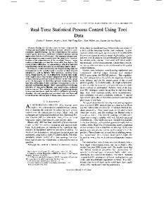
The I-ITS downconverLer is shown in Fig. 1: tic block diagram is shown in Fig. 2. It consists of an HTS prc-scleet fi]tcr, a cryogenic low-noise amplifier (LNA) using HEMTs (High F.lectron MobiliLy Transistors), a cryogenic diode mixer, and a cryogenic FET osciltmor with an I-ITS resonator. I“hc local oscillator (LO) is 8.4 GHz and mixes with the input signal to produce the inLcrmcdiaLc frequency (IF) output around 1 G}iz, The. input frequency band is 7.25 to 7.45 G}lz, which is near certain NASA uplink frequencies used for deep space communications. The 8.4 GHz oscillator frequency corresponds [o a dowrdink transmission frequency and is typical of the LO in a deep space transponder. Although a spacccrafL transponder is considerably more complex than this downconvcrtcr subsystem, the components to be inLcgrated and the necessary integration techniques arc representative of spacecraft requirements and would form a basis for introducing HTS matcriai inLo clthcr portions of a transponder subsystcm.
?
2156--14
Introduction of HTS material into the pm-select filter reduces losses in front of the LNA to improve the noise figure significamly compared to a filter of normal metal film. An HTS resonator provides a higher ‘(Q for the oscillator, producing a mom stable frequency output and lower phase noise than a lower “Q” nomml rncml film resonator could, The layout of the downconvmtcr is shown in Fig. 1. The HIS film is YBa 1.95Lao,
[email protected] (YBLCO) deposited on lanthrmum aluminate (LaA103) substrates. In Fig. 1 the YBLCO is black with some gold pads: the transparent lanthanum aluminate substrates appear darker than the white alumina substrates in the photograph because of the ground plane metalli-zation on their bottom surfaces. The LNA and mixer circuits use gold film on alumina substrates. The receiver components arc integrated into a single hermetic package designed for space qualification and minimal intra-cavity RF interference. The package is machined from Kovar (ASTM F] 5 alloy) and nickel- and gold-plated. Descriptions of the individual downconverter components follow. 2.1.
Superconducting pre-select fiiter
The superconducting pre-select filter is a microstrip circuit on a 15.0 x 7 x 0.51 mm lanthanum aluminate sut)strate. The patterned microstrip conductor on the top surface is a thin film of superconducting YBLCO. Low-rcsistmce gold contact bonding pads arc deposited over the YBLCO (using an in-situ process) at the input and output, and at test bonding sites along the edges of the substrate. The ground plane on the bottom surface of the substrate is Nb-Cu-Au metal fihn. The filter is a 4-pole parallel-coupled-line microstrip dcsigri with half-wavelength resonators (Fig. 3). The center frequency is 7.3S GHz with a -3-dB bandwidth of 400 MHz,. In this SLi”ucturc, the narrowness of the passband and the number of poles is constrained by the desired area of the filter, The estimated insertion loss for the HTS filter alone is 0.2 to 0.3 dB at 77 K, an improvement of over 0.5 dB compared to a copper film version of the filter at the same temperature. 2.2.
Low-noise amplifier (LNA)
The LNA consists of two stages, each using a GaAs-based FujiLNr FHX15X HEMT (High Etectron Mobility Transistor) chip device. The first stage is designed for optimum noise figure at cryogenic temperatures. The second stage is designed for gain and to flatten the response of the two stages together. The dc.sign of the LNA is shown in Fig. 4. It uses rnicrostrip circuitry wi~h TiW-Au mctailization on alumina substrates. Matching is performed for both stages by usc of quarter-wave transformers. Bias is supplied at the gate by tying a high impedance l/4-wave line to the transformer. Drain voiLlgc is conrw.ctcd by wire bond from the stabilizing resistor to the output matching section. A coupled-line section is placed at the output of each stage for blocking of DC voltages, The filter acts as a DC block for the amplifier input. Tuning pads were placed adjacent to transmission lines and wire bonds were tied from the transmission lines to appropriate pads to improve response. The amplifier modules were tested at 77 K physical temperature prior to integration with other sub-modules. The noise temperature nwasured at the refrigerator port, which includes the cffc.ct of refrigerator input coaxial cables and test fixture 10S.SCS, was less than 44 K in the downconvcrtcr passband. The gain was 28 dB. 2.3.
Superconducting
Oscillator
The local oscillator is a GaAs MESFET-based, reflection mode circuit implemented as a hybrid microwave integrated circuit. The circuit (Fig. 5) consists of a single lanthanum aluminate substrate on which passive elements of the circuit (stabilizing resonator, reactive feedback ciemcnts, transmission lintx, and DC bias Iincs) are realized as microstrip eiemcnts etched from an HTS film deposited on the top surface. Ile conductor layers are as described for the prc-.sdcct filter. The GaAs MESFET (Avantek ATF- 13100-GP1 chip), which is the active clcmcnt of the circuit, is a[tachcd to the substrate using a conductive epoxy. Gold bond wires connect the MESFET and the superconducting lines; gold contact pacts sputtered cm the superconducting lines provide low resistance contact. Chip capacitors and resistors mounted next to the substrate are used to filter and de-couple the tmnsistor him. The design of the oscillator represented a compromise kctwrxn circuit p-formancc and constraints for HTSSE-11. Design
,.
1
2156-14
considerations for this oscillator included minimizing size for integration, minimizing power dissipation in the cryogenic package (to tens of row), providing enough RF power to drive the mixer (O to 3 dBm), and minimizing phase noise. Although an oscillator using a resonator in the transmission mode (a 2-port resonator) should be less sensitive to load pulling, and bias drift and ripple, a design using a resonator in the reflection mode (a l-port resonator) was chosen to minimize complexity, size, and power dissipation. A linear rcsorwtor coupled to the output line was used. The output of the oscillator is near 8.4 GHz with output power levels of up to +10 dBm (into a 50 Q load). Typical operating conditions for the oscilL~tor when incorporated into the downconverter provide O to +3 dBm of output power with