Jun 9, 2006 - exhibits an asymmetry related to the 0.7 structure in conductance. The asymmetry in ... and theory [15, 16] suggest that 0.7 structure is a many-.
Shot-Noise Signatures of 0.7 Structure and Spin in a Quantum Point Contact L. DiCarlo∗ , Y. Zhang∗ , D. T. McClure∗ , D. J. Reilly, C. M. Marcus Department of Physics, Harvard University, Cambridge, Massachusetts 02138, USA
arXiv:cond-mat/0604019v2 [cond-mat.mes-hall] 9 Jun 2006
L. N. Pfeiffer, K. W. West Bell Laboratories, Lucent Technologies, Murray Hill, NJ 07974, USA (Dated: February 6, 2008) We report simultaneous measurement of shot noise and dc transport in a quantum point contact as a function of source-drain bias, gate voltage, and in-plane magnetic field. Shot noise at zero field exhibits an asymmetry related to the 0.7 structure in conductance. The asymmetry in noise evolves smoothly into the symmetric signature of spin-resolved electron transmission at high field. Comparison to a phenomenological model with density-dependent level splitting yields good quantitative agreement.
Shot noise, the temporal fluctuation of current resulting from the quantization of charge, is sensitive to quantum statistics, scattering and many-body effects [1, 2]. Pioneering measurements [3, 4, 5] of shot noise in quantum point contacts (QPCs) observed the predicted [6] suppression of shot noise below the Poisson value due to Fermi statistics. In regimes where many-body effects are strong, shot noise measurements have been exploited to directly observe quasiparticle charge in strongly correlated systems [7, 8, 9] as well as to study coupled localized states in mesoscopic tunnel junctions [10] and cotunneling in nanotube-based quantum dots [11]. Paralleling these developments, a large literature has emerged concerning the surprising appearance of an additional plateau in transport through a QPC at zero magnetic field, termed 0.7 structure. Experiment [12, 13, 14] and theory [15, 16] suggest that 0.7 structure is a manybody spin effect. Its underlying microscopic origin, however, remains an outstanding problem in mesoscopic physics. This persistently unresolved issue is remarkable given the simplicity of the device. In this Letter, we report simultaneous measurements of the shot noise at 2 MHz and dc transport in a QPC, exploring the noise signature of the 0.7 structure and its evolution with in-plane magnetic field Bk . A suppression of the noise relative to that predicted by theory for spindegenerate transport [6] is observed near 0.7 × 2e2 /h at Bk = 0, in agreement with results from Roche et al. [14] obtained at kHz frequencies. This suppression evolves smoothly with increasing Bk into the signature of spinresolved transmission. We find quantitative agreement between noise data and a phenomenological model for a density-dependent level splitting [16], with model parameters extracted solely from conductance. Measurements are performed on a gate-defined QPC fabricated on the surface of a GaAs/Al0.3 Ga0.7 As heterostructure grown by molecular beam epitaxy (see mi-
∗ These
authors contributed equally to this work.
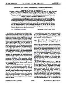
FIG. 1: Equivalent circuit near 2 MHz of the noise detection system measuring QPC noise by cross-correlation on two amplification channels [17]. The scanning electron micrograph shows a device of identical design to the one measured. The QPC is formed by negative voltages Vg1 and Vg2 applied on two facing electrostatic gates. All other gates on the device are grounded.
crograph in Fig. 1). The two-dimensional electron gas 190 nm below the surface has a density of 1.7 × 10⁻¹¹ cm−2 and mobility 5.6 × 106 cm2 /Vs. All data reported here were taken at 290 mK, the base temperature of a 3 He cryostat. The differential conductance g = dI/dVsd (where I is the current and Vsd is the source-drain bias) is measured by lock-in technique with an applied 25 µVrms excitation at 430 Hz [17]. The resistance Rs in series with the QPC is subtracted at every applied Bk (see Fig. 2(a)) [18]. The QPC is first characterized at zero and finite Bk using dc conductance measurements. Figure 2(a) shows linear-response conductance g0 = g(Vsd ∼ 0) as a function of gate voltage Vg2 , for Bk = 0 to 7.5 T in steps of 0.5 T. The QPC shows the characteristic quantization of conductance in units of 2e2 /h at Bk = 0, and the appearance of spin-resolved plateaus at multiples of 0.5 × 2e2/h at Bk = 7.5 T. Additionally, at Bk = 0, a shoulder-like 0.7 structure is evident, which evolves smoothly into the 0.5 × 2e2 /h spin-resolved plateau at high Bk . Figures 2(b) and 2(c) show g as a function of Vsd for evenly spaced Vg2 settings at Bk = 0 and 7.5 T, respectively. In this representation, linear-response plateaus in Fig. 2(a) appear as accumulated traces around Vsd = 0 at multiples of 2e2 /h for Bk = 0, and at multiples of 0.5 × 2e2 /h for Bk = 7.5 T. At finite Vsd , additional
2 capacitor resonator that performs current-to-voltage conversion. Each channel consists of a transconductance stage using a high electron mobility transistor (HEMT) cooled to 4.2 K, followed by 50 Ω amplification at room temperature. The amplified noise signals from both channels are sampled simultaneously by a digitizer, and their cross-spectral density calculated by fast-Fouriertransform. The cross-spectral density is maximal at resonance, with a value ! �2 � Reff 0 2 P + 4kB Te Reff , (1) XR = GX SI 1 + gRs
FIG. 2: (color) (a) Linear conductance g0 as a function of Vg2 (Vg1 = −3.2 V), for Bk ranging from 0 (red) to 7.5 T (purple) in steps of 0.5 T. The series resistance Rs ranging from 430 Ω at Bk = 0 to 730 Ω at Bk = 7.5 T has been subtracted to align the plateaus at multiples of 2e2 /h. (b,c) Nonlinear differential conductance g as a function of Vsd , at Bk = 0 (b) and 7.5 T (c), with Vg2 intervals of 7.5 and 5 mV, respectively. Shaded regions indicate the bias range used for the noise measurements presented in Figs. 3(b) and 4.
plateaus occur when a sub-band edge lies between the source and drain chemical potentials [19]. The features near 0.8 × 2e2 /h (Vsd ≈ ±750 µV) at Bk = 0 cannot be explained in the context of a single-particle picture [12, 15]. These features are related to the 0.7 structure around Vsd = 0 and resemble the spin-resolved finite bias plateaus at ∼ 0.8 × 2e2 /h for Bk = 7.5 T [12]. Turning now to noise measurements, we consider the QPC noise in excess of thermal noise 4kB Te g(Vsd ). When 1/f and telegraph noise as well as bias dependent heating are negligible (as shown to be the case in these data) the excess noise is dominated by noise arising from the partitioning of electrons at the QPC, which we denote as partition noise, SIP (Vsd ) = SI (Vsd ) − 4kB Te g(Vsd ), where SI is the total QPC current noise spectral density. Note that SIP is noise in excess of 4kB Te g(Vsd ) rather than 4kB Te g(0) as considered in Refs. [3, 14]. We measure SIP near 2 MHz using the cross-correlation technique shown schematically in Fig. 1 to suppress amplifier voltage noise [4, 17]. Two parallel channels amplify the voltage fluctuations across a resistor-inductor-
where GX is the geometric mean of the voltage gain of the amplification channels, Te is the electron temperature and Reff is the effective resistance (at 2 MHz) between the HEMT gates and ground. Reff is measured from the half-power bandwidth of the cross-spectral density [17]. SIP is extracted from simultaneous measure0 ments of XR , g and Reff following calibration of GX and Te using thermal noise. At Vsd = 0, where SIP van0 ishes, XR = G2X · 4kB Te Reff . At elevated temperatures (3 to 5 K), where electrons are well thermalized to a 0 calibrated thermometer, a measurement of XR as a function of Reff (tuned through Vg2 ) allows a calibration of GX = 790 V/V. This gain is then used to determine from similar measurements the base electron temperature Te = 290 mK. Figure 3 shows SIP (Vsd ) at Bk = 0 and fixed Vg2 for Vsd between −150 µV and +150 µV (blue regions in Figs. 2(b) and 2(c)). With an integration time of 60 s at each bias point, the resolution in SIP is 1.4×10⁻²⁹ A2 /Hz, equivalent to full shot noise 2eI of I ∼ 40 pA. Open markers superimposed on the linear conductance trace in Fig. 3(a) indicate Vg2 settings for which corresponding noise data are shown in Fig. 3(b). SIP vanishes with the QPC pinched off (g(Vsd ) = 0), or on linear conductance plateaus, which shows that bias-dependent electron heating is not significant [4]. In contrast, for g ≈ 0.5 and 1.5 × 2e2 /h, SIP grows with |Vsd | and shows a transition from quadratic to linear dependence [3, 4, 5], demonstrating the absence of noise from resistance fluctuations. Solid curves superimposed on the SIP (Vsd ) data in Fig. 3(b) are fits to the form SIP (Vsd )
� � � � eVsd 2e2 N eVsd coth − 2kB Te , (2) =2 h 2kB Te
with the noise factor N as the only free fitting parameter. Note that N relates SIP to Vsd , in contrast to the Fano factor, which relates SIP to I [1, 2]. The form of this fitting function is motivated by mesoscopic scattering theory [1, 2, 6], where transport is described by transmission coefficients τn,σ (n is the transverse mode index and σ denotes spin) and partition noise originates from
3
2
(b)
0.3
2
(a)
Data
Model
Single Particle B|| = 0T
0 1
2
-1700
-1100
0
Vg2 [mV]
2
]An e2[
S I
P
0
1
2
I
P
S
(c)
N
g
0
0 0
0
0.2
2
]An e2[
2
]h / e2[
(a)
0.1
0.0 0 2
dg/dVg2 [e / (h V)]
0
-1
0
1
0
mV]
2
(c) 2
1
Data
0
Model
g
Bk = 0. Markers indicate Vg2 settings for the noise measurements shown in (b) and (c). (b) Measured SIP as a function of Vsd , for conductances near 0 (red), 0.5 (orange), 1 (green), 1.5 (blue), and 2 ×2e2 /h (purple). Solid lines are best-fits to Eq. (2) using N as the only fitting parameter. In order of increasing conductance, best-fit N values are 0.00, 0.20, 0.00, 0.19, and 0.03. (c) SIP as a function of dc current I with the QPC near pinch-off. The dotted line indicates full shot noise SIP = 2e|I|, comparable to results in Ref. [20].
(b)
2
FIG. 3: (color) (a) Linear conductance g0 as a function of Vg2 at
-1000
1 2 gavg [2e / h]
]h / e2[
Vsd [
100
30
]Vm[ 2gV
I [nA]
-100
0
-1500
Single Particle 0 -1
0
-1500
1
Vsd [mV]
(d)
Data
0.2
-1250
-1000
Vg2 [mV]
Model
(e)
0T
0T
N 0.1
the partial transmission of incident electrons. Within scattering theory, the full expression for SIP is 2e2 SIP (Vsd ) = h
Z X n,σ
7.5T 7.5T 0.0 0
τn,σ (ε)(1 − τn,σ (ε))(fs − fd )2 dε,
(3) where fs(d) is the Fermi function in the source (drain) lead. Eq. (2) follows from Eq. (3) only for the case of constant transmission across the energy window of transport, P with N = 12 τn,σ (1 − τn,σ ). For spin-degenerate transmission, N vanishes at multiples of 2e2 /h and reaches the maximal value 0.25 at odd multiples of 0.5 × 2e2 /h. We emphasize that while Eq. (2) is motivated by scattering theory, the value of N extracted from fitting with Eq. (2) simply provides a way to quantify the SIP (Vsd ) for each Vg2 . We have chosen the bias range e|Vsd | . 5kB Te for fitting N to minimize the effects of nonlinear transport while extending beyond the quadratic-to-linear crossover in noise that occurs on the scale eVsd ∼ 2kB Te . The dependence of noise factor on QPC conductance at Bk = 0 is shown in Fig. 4(a), where N is extracted from measured SIP (Vsd ) at 90 values of Vg2 . The horizontal axis, gavg , is the average of the differential conductance over the bias points where noise was measured. N has the shape of a dome, reaching a maximum near odd multiples of 0.5 × 2e2/h and vanishing at multiples of 2e2 /h. The observed N (gavg ) deviates from the spin-degenerate, energy-independent scattering theory in two ways. First, there is a reduction in the maximum amplitude of N
2
gavg [2e / h]
1 0
2
1
gavg [2e / h]
FIG. 4: (color) (a) Experimental N as a function of gavg at Bk = 0 (red circles) along with model curves for nonzero (solid) and zero (dashed) proportionality of splitting, γn (see text). (b) Transconductance dg/dVg2 as a function of bias voltage Vsd and gate voltage Vg2 . Blue lines trace the alignment of sub-band edges with source and drain chemical potentials; their slope and intersection give the conversion from Vg2 to energy and the energy spacing between modes, respectively [22, 23]. (c) Measured linear conductance (red) as a function of Vg2 at Bk = 0, and linear conductance calculated with the model (black solid) with best-fit values for ωx and γn . Single-particle conductance model takes γn = 0 (black dashed). (d) Experimental N as a function of gavg in the range 0 − 1 × 2e2 /h, at Bk = 0 T (red), 2 T (orange), 3 T (green), 4 T (cyan), 6 T (blue), and 7.5 T (purple). (e) Model curves for N (gavg ) (see text). Dashed curves in (d) and (e) show the singleparticle model (γn = 0) at zero field for comparison.
below 0.25. Second, there is an asymmetry in N with respect to 0.5 × 2e2 /h, resulting from a noise reduction near the 0.7 feature. A similar but weaker asymmetry is observed about 1.5 × 2e2 /h. The dependence of N (gavg ) on Bk is shown in Fig. 4(d). N is seen to evolve smoothly from a single asymmetric dome at Bk = 0 to a symmetric double-dome at 7.5 T, the latter a signature of spin-resolved electron transmission. Notably, near 0.7 × 2e2 /h, N appears insensitive to Bk ,
4 in contrast to the dependence of N near 0.3 × 2e2 /h. We find that all features in noise data are well accounted for within a simple phenomenological model in which the twofold degeneracy of QPC mode n is lifted by a splitting ∆εn,σ = σ · ρn · γn , that grows linearly with 1D density ρn (with proportionality P √ γn ) within that mode. Here, σ = ±1/2 and ρn ∝ σ µ − εn,σ , (µ is the chemical potential). The lever arm converting from Vg2 to energy (and hence ρn ) as well transverse mode spacing are extracted from transconductance (dg/dVg2 ) data (Fig. 4(b)). Assuming an energy-dependent transmission, τn,σ (ε) = 1/(1 + e2π(εn,σ −ε)/~ωx ), appropriate for a saddle-point potential with curvature parallel to the current described by ωx [21], the value for ωx is found by fitting linear conductance below 0.5 × 2e2 /h (below 1.5 × 2e2 /h for the second mode), and γn is obtained from a fit to conductance above 0.5(1.5) × 2e2 /h, where (within the model) the splitting is largest (see Fig. 4(c)). For the QPC studied, we find ~ωx is ∼ 500(300) µeV and γ1(2) ∼ 0.012(0.008) e2 /4πǫ0 for the first (second) transverse modes. Note that the splitting is two orders of magnitude smaller than the direct Coulomb energy of electrons spaced by 1/ρn . Using these parameters, model values for SIP (Vsd ) are then calculated using the full Eq. (3), and N is extracted by fitting the model SIP (Vsd ) to Eq. (2). The resulting model values of N (gavg ) at Bk = 0 are shown along with the experimental data in Fig. 4(a). Also shown for comparison are the model values only accounting for energy dependent transmission but no splitting (γn = 0). The overall reduction of N arises from a variation in transmission across the 150 µV bias window, which is comparable to ~ωx . Asymmetry of the model values for N about 0.5 and 1.5 × 2e2 /h require nonzero γn . We include magnetic field in the model with corresponding simplicity by assuming a g-factor of 0.44 and adding the Zeeman splitting to the density-dependent splitting [24] maintaining the parameters obtained above. The resulting model values for N are shown in Fig. 4(e), next to the corresponding experimental data (Fig. 4(d)). Experimental and model values for N show comparable evolution in Bk : the asymmetric dome at Bk = 0 evolves smoothly into a double dome at 7.5 T, and for conductance & 0.7 × 2e2 /h, the curves for all magnetic fields overlap closely. Some differences are observed between data and model, particularly for Bk = 7.5 T. While the experimental double-dome is symmetric with respect to the minimum at 0.5 × 2e2 /h, the theory curve remains slightly asymmetric with a less pronounced minimum. We find that setting the g-factor to ∼ 0.6 in the model reproduces the measured symmetrical double-dome as well as the minimum value of N at 0.5 × 2e2 /h. This observation is consistent with previous reports of an enhanced g-factor in a QPC at low-density [12]. We thank H.-A. Engel, M. Heiblum, L. Levitov and
A. Yacoby for valuable discussions, and S. K. Slater, E. Onitskansky and N. J. Craig for device fabrication. We acknowledge support from NSF-NSEC, ARO/ARDA/DTO and Harvard University.
[1] Ya. M. Blanter and M. B¨ uttiker, Phys. Rep. 336, 1 (2000). Ya. M. Blanter, cond-mat/0511478 (2005). [2] T. Martin, in Nanophysics: Coherence and Transport, Les Houches Session LXXXI, edited by H. Bouchiat et al. (Elsevier, Amsterdam, 2005), cond-mat/0501208. [3] M. Reznikov et al., Phys. Rev. Lett. 75, 3340 (1995). [4] A. Kumar et al., Phys. Rev. Lett. 76, 2778 (1996). [5] R. C. Liu et al., Nature 391, 263 (1998). [6] G. B. Lesovik, Pis’ma Zh. Eksp. Teor. Fiz. 49, 513 (1989). [JETP. Lett. 49, 592 (1989)]; M. B¨ uttiker, Phys. Rev. Lett. 65, 2901 (1990). [7] R. de-Picciotto et al., Nature 389, 162 (1997); M. Reznikov et al., Nature 399, 238 (1999). [8] L. Saminadayar et al., Phys. Rev. Lett. 79, 2526 (1997). [9] X. Jehl et al., Nature 405, 50 (2000). [10] S. S. Safonov et al., Phys. Rev. Lett. 91, 136801 (2003). [11] E. Onac et al., Phys. Rev. Lett. 96, 026803 (2006). [12] K. J. Thomas et al., Phys. Rev. Lett. 77, 135 (1996); A. Kristensen et al., Phys. Rev. B 62, 10950 (2000); D. J. Reilly et al., Phys. Rev. B 63, 121311(R) (2001); S. M. Cronenwett et al., Phys. Rev. Lett. 88, 226805 (2002); D. J. Reilly et al., Phys. Rev. Lett. 89, 246801 (2002); [13] W. D. Oliver, Ph.D. Dissertation, Stanford University (2002). [14] P. Roche et al., Phys. Rev. Lett. 93, 116602 (2004). [15] C. K. Wang and K.-F. Berggren, Phys. Rev. B 54, 14257 (1996); H. Bruus, V. V. Cheianov and K. Flensberg, Physica E 10, 97 (2001); Y. Meir, K. Hirose and N. S. Wingreen, Phys. Rev. Lett. 89, 196802 (2002); K. A. Matveev, Phys. Rev. Lett. 92, 106801 (2004); A. Ramˇsak and J. H. Jefferson, Phys. Rev. B 71, 161311(R) (2005). [16] D. J. Reilly, Phys. Rev. B 72, 033309 (2005). [17] L. DiCarlo et al., cond-mat/0406018 (2006). [18] A 125 mT perpendicular magnetic field is applied throughout to minimize bias-dependent electron heating [4]. Perpendicular fields of this size do not affect the main results presented here. [19] L. P. Kouwenhoven et al., Phys. Rev. B 39, 8040(R) (1989). [20] Y. Chen and R. A. Webb, Phys. Rev. B 73, 035424 (2006). [21] M. B¨ uttiker, Phys. Rev. B 41, 7906(R) (1990). [22] N. K. Patel et al., Phys. Rev. B. 44, 10973(R) (1991). [23] Two crossing points are observed at finite bias between the first and second modes. The model attributes this to spin splitting in the first mode. The midpoint is taken as the crossing point for the blue lines. [24] In the measurement regime investigated, various ways of adding Zeeman splitting to zero-field splitting (linearly, quadrature, thermally weighted) give essentially indistinguishable results within the present model.