(1973), Selberherr (1984) and Snowden (1986). In general terms, these models require the self-consistent solution of the following equations1 ...
291
SIMULATION OF SEMICONDUCTOR DEVICES AND PROCESSES Vol. 3 Edited by G. Baccarani, M. Rudan - Bologna (Italy) September 26-28,1988 - Tecnoprint
Simulation of Non-Planar GaAs Devices PJ. Haigh, R.E. Miles, CM. Snowden Microwave Solid State Group, Department of Electrical and Electronic Engineering, University of Leeds, Leeds, England.
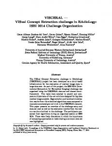
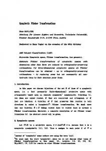
Abstract A comprehensive numerical simulation has been developed in order to obtain a greater understanding of the operation and limitations of nonplanar devices. The simulation employs a new, extremely flexible finitedifference scheme which is capable of fitting a two dimensional mesh to any user defined device domain. The simulation has been used to analyse a coplanar varactor diode, results for which are presented.The model has been extended to investigate the effects of surface states on device performance. Introduction The development of monolithic microwave integrated circuits (MMICs) has stimulated particular interest in surface orientated GaAs devices. These devices frequently require intricate, non-planar geometries and complex doping profiles. For example, a coplanar varactor diode has been developed for inclusion in an MMIC oscillator where the topology complements that of the surface orientated GaAs MESFET (fig, 1). The capacitance-voltage characteristics of these devices depend directly on the donor doping profile of the epitaxial layer and in order to obtain a maximum capacitance change, a hyperabrupt doping profile is often used (fig. 2). At high bias, the edge of the depletion region is pushed into the low doped region of the epitaxial layer. The sloping sidewall, which is produced by selective etching, was developed to limit the sideways spread of the depletion region at these bias voltages and limit the resulting capacitance change.
?92
Schottky .Epitaxial Layer Ohmic
Ohmic
'
•/////\
N+
1/////V
+
Fig. 1 Coplanar varactor diode
0.4
5.5 0.6 Depth {micron]
0.7
Fig. 2 Doping Profile of A Typical Hyperabrupt Varactor Diode. The numerical simulation presented here was developed in order to obtain a greater understanding of the physical operation of non-planar GaAs devices such as the coplanar varactor and the model may be used to predict both the D.C., transient and R.F. characteristics. Further, the ability to model arbitrary geometry devices allows the evaluation of complex structures prior to fabrication. The Classical Semiconductor Equations The majority of physical device models, where the dimensions of the device geometry are greater than 1 fj.ni employ the classical semiconductor equations. These equations have been derived, both rigorously and heuristically, from the Boltzmann transport equations by several workers, Reiser (1973), Selberherr (1984) and Snowden (1986). In general terms, these models require the self-consistent solution of the following equations1
293
Poisson's equation: V ^ = —2_(Afo - n)
(1)
£oer
where tjj is the electrostatic potential, q is the electronic charge, e0er is the permittivity, Np is the donor doping density and n is the electron concentration. Current continuity: f- = ±VJH + G (2) at q where Jn is the electron density and C is the generation-recombination rate, which in most unipolar devices such as MESFETs and Schottky varactor diodes is assumed to be negligible for normal operating conditions. Current density: J„ = qnv„ + qD„Vn (3) where v„ is the electron drift velocity and D„ is the electron diffusion coefficient. The diffusion coefficient, Dn, is often defined in terms of the Einstein relationship. kT Dn = —-Hn (4) q
where k is the Boltzmann constant and T is the lattice temperature. Frequently, the drift velocity term in equation (4) is replaced by: v„ = -n„E (5) where, the electric field E = -Vtf
(6)
The current, I associated with the contact of the semiconductor device is obtained by intergrating the total current density, J across a suitable surface surrounding the'contact. / = / Ids
(7)
s
The total current density, J includes both the particle current, J„ and the displacement current dE J = J„ + er£d~^(S) Unipolar devices such as MESFETs and Schottky varactor diodes are usually analysed using a single species set of the basic transport equationsowever, the treatment for holes is entirely analogous.
294
The physical model described by these equations is subject to three main assumptions. These are that the carrier velocities respond instantaneously to changes in the electric field and that the mobility and diffusion coefficients are functions of the electric field alone. In practice, this seems to be an adequate approximation in circumstances where the electric field is changing slowly with time and space. The mobility and diffusion coefficients are dependent on several parameters (for example electron temperature, carrier concentration and electric field) (Doades,1984, Snowden,1986). The influence of hot electron effects in smaller geometry devices is discussed elsewhere (for example, Snowden, 1987). Modelling of the boundary conditions The domain of the device model is defined by the geometry chosen to represent the actual device. The surface orientated nature of non-planar devices requires a two dimensional model to account for the non-uniform nature of the electric field and electron distribution. The boundary of the simulation domain consists of two components; real "physical" boundaries such as contacts and free surfaces and internal boundaries which limit the device domain within the semiconductor. Schottky Contacts The simulation incorporates a sophisticated Schottky contact model which is capable of modelling accurately both thermionic and thermionicfield emissions. The ]j£ component is expressed in terms of an effective recombination velocity, vr and a quasi-equilibrium electron density n0. Jre =q("s ~n0)vr
(9)
where ns is the electron concentration on the semiconductor side of the Schottkv contact. The effective recombination velocity is given by (Sze,1981). A'T2
* - it
m
where A * is the effective Richardson constant and Nc is the effective density of states in the conduction band (Sze,1981). The quasi-equilibrium electron density is obtained from 4>bn 01) n0 = Nc.exp ' kT where qbn is the barrier height and k is the Boltzmann constant. The potential fa at the Schottky barrier interface is *s = VA-