Dongku Kang, Mark C. Johnson and Kaushik Roy. School of Electrical and Computer Engineering. Purdue University. West Lafayette, Indiana, 47907-1285.
Simultaneous Multiple-V Scheduling and Allocation for Partitioned Floorplan Dongku Kang, Mark C. Johnson and Kaushik Roy School of Electrical and Computer Engineering Purdue University West Lafayette, Indiana, 47907-1285 dkang,mcjohnso,kaushik�@purdue.edu Abstract In this paper, we propose a simultaneous scheduling and allocation algorithm for voltage-partitioned multiple-V design. By considering voltage partition during scheduling and allocation, we may place the resources of same voltage in one partition, thereby reducing additional power meshes. Also, the partitioned design reduces the energy dissipation of level converters by reducing cutsize between differentvoltage partitions. The proposed algorithm starts from a random solution. Then, it performs scheduling and allocation simultaneously while trying to satisfy both resource and time constraints. By gradually changing the schedule and allocation, the algorithm effectively explores solution spaces to achieve low-power and better partitioning in terms of the supply voltages. Relative to the minimum single voltage design, 36% of energy saving was achieved. Also, improvements for interconnect, level-conversion energy, and voltage clusters were observed.
1 Introduction Power consideration is an important design issue for the modern portable devices. For static CMOS circuits, energy dissipation is dominated by switching power, which is proportional to the square of the supply voltage as shown in Eq.1, where �, �� , and ���� denote switching activity, load capacitance, and operating frequency.
����
�� ¾ �� ����
(1)
Among various technologies for low-power, voltage scaling is an effective technique to reduce the energy dissipation. However, reduced supply voltage results in the increased propagation delay [1]. Therefore, the global reduction in supply voltage slows down the speed of the circuits,
0-7695-2093-6/04 $20.00 2004 IEEE
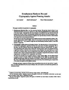
Clock-cycle
Clock-cycle
+
+
2.5V
4
1
1
+
2.5V Extract extra time slack
2
1
Unused Slack
2
+
2.5V
2.5V
4
Multiple-Vdd Scheduling
2.5V
3
3
(a)
4
2
2.5V
3
1.78V 2.5V
(b)
Figure 1. A DFG and multiple-V
(c)
scheduling
thereby degrading the computational throughput. To maintain the computational throughput with reduced energy dissipation, multiple-V design was introduced. In multipleV design, a lower supply voltage is applied to the circuits that can be slowed down, while a higher voltage supply is applied to the circuits in the critical paths. For data-flow graphs (DFG), non-uniform path lengths can result in timing slacks in schedule. In Fig.1, node and edge represent operation and data transfer in DFG. As an example, node 4 can be scheduled in either first or second clock-cycle because the result of node 4 is necessary for node 3, which is scheduled in the third clock-cycle. Using the unused time slack, we can schedule node 4 in the lower voltage resource, which has two clock-cycle delay. Therefore, by scheduling nodes with unused time slack in the lower voltage resources, one can reduce the energy dissipation while maintaining the computational throughput. Various efforts related to the multiple-V design have been made. Usami and Horowitz [2] proposed a design technique to reduce the energy consumption in a circuit by using two supply voltages. The gates on the critical paths are operated at the higher supply voltage, while the gates on the non-critical paths are at the lower supply voltage. Chang and Pedram [3] proposed an algorithm to minimize the energy dissipation in high-level synthesis with time con-
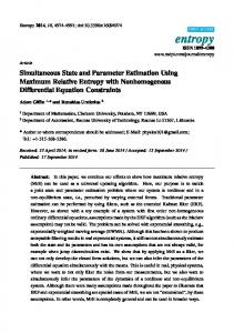
VDD1 VDD2
VDD1
VDD1
VDD1 VDD2
VDD2 VDD1
VDD2
VDD1
VDD1 VDD2
VDD1 VDD2
VDD1
VDD1
VDD2 VDD2
1
2
1
2
3
4
3
4
(a)
Non-partitioned
Figure 3. Possible movements in the partitioning algorithms. (a) K-KL (b) K-PM/FM
Figure 2. The concept of the voltagepartitioned design.
source and time constraints. Also, K-KL reduced the energy and number of level converters. Furthermore, it generated a floorplan, which is well partitioned by the supply voltages.
straint. Johnson and Roy [4] used an integer-linear programming (ILP) formulation with the resource and time constraints. Sarrafzadeh and Raje [5] proposed a dynamic programming approach. Manzak [6] presented scheduling algorithms with resource and time constraints with low complexity. However, there exist several disadvantages when we design using multiple-V . First, if we do not partition the voltage domains, then we are forced to either interleave the power rails or use an additional metal layer as shown in Fig.2. Second, we have to consider extra communication cost due to the level converter. Third, there may be noise issues. When two interconnects which operate at different logic levels are coupled, there can be a cross-talk problem. Also, when the higher voltage circuits inject larger amount of current into the substrate, the noise tolerance of lower voltage circuits will be affected. Therefore, to realize multiple-V design, we need additional considerations other than module energy dissipation. By removing the edges between different voltage domains in a DFG, we can reduce the interactions between the resources that operate in the different voltage domains. Hence, we can separate resources with respect to the supply voltage. Also, when generating a floorplan, the reduced interactions between different voltage resources will promote the voltage-partitioned floorplan as shown in Fig.2, which is well partitioned by their respective supply voltage. Furthermore, when the edges between different supply voltages are removed, we can reduce the energy dissipation due to the level converter. Recently, Kang et al. [7] presented a scheduling and allocation scheme for voltage partitioned floorplan, which is based on the graph-partitioning problem [8], [9]. They generated an initial schedule to determine the supply voltages for each resource. Also, nodes are allocated to serve as an initial solution for partitioning algorithm. By swapping supply voltages for pairs of nodes, the modified KernighanLin algorithm (K-KL) [7] minimized the number of edges between different supply voltages, while maintaning the re-
In this paper, we present a different approach for the voltage-partitioned multiple-V design, which does scheduling and allocation simultaneously. Starting from a random allocation, proposed partitioning algorithm changes the schedule and the allocation for better partitioning. Also, to reduce the energy dissipation, it schedules as many nodes as possible to lower voltage resources. For partitioning, we adapted Fiduccia-Mattheyses algorithm (FM) [10], which moves a single node at a time. To decide movements for each node, we calculate gains for each node. When moving a node that maximizes the gain, the resource allocation is modified. Then, a list scheduler quickly generates a schedule with the allocation defined by the partitioning algorithm. Compared to ���¿ � complexity of [7], the proposed algorithm shows ���¾ � complexity. When resource constraints are larger than two, the partitioning problem becomes multiway partitioning. In the previous work [7], by calculating gains for pair-swapping movements, it considered all possible movements between all possible resources. Here, we adopted the scheme proposed in [11], which limits the movements between two specific resources. In Fig.3(a) , a node in resource 1 can be exchanged with a node in any resource. But in (b), a node in resource 1 can move to the resource 2 regardless of the existence of an exchangeable node. But, the movement to the resource 3 or 4 is prohibited in this pass. The rest of the solution space will be explored in the next passes. Comparing to [7], the worst case number of directions are reduced from ��� �� ��� to ��� �. We easily observe that � � pairs are selected out of � �� �� �. Important decision in each pass is: how to pair resources? In our formulation, random pairing scheme is used. The remainder of this paper is organized as follows; Section 2 presents the problem formulations for the proposed methodology. Section 3 describes the overall algorithm to schedule and allocate nodes in a DFG. Section 4 contains experimental results. Finally, Section 5 shows final remarks on this work. 2
0-7695-2093-6/04 $20.00 2004 IEEE
(b)
Partitioned
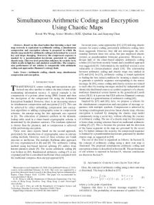
Resource
r1
r2
1
5
r3
r1
6
5
2
6
4 (b)
Resource
r1
2
6
3
4
1 1
4 Clock-cycle
6
r3
r2
3
1
Resource
5
r3
r3 r2
2
Resource
2
4
3
r2
5
r1
1
5 6 Clock-cycle
2
1
3
2
4
4 Clock-cycle (b)
3
(a)
3 4
r3
2.5V
2.5V
1.78V
r2
5
6
r1
1
2
Figure 5. Energy gain example.
3 4
(a) (c)
r1
4 Clock-cycle
r3
r2
5
1 w2
2 w3
Figure 4. Clock-cycle gain example.
4 2.5V
6
3 2.5V
1.78V
- Logic Level-Converter
2 Formulations 2.1 Basics
Figure 6. Cutsize gain example.
Suppose nodes in a DFG are partitioned into K non-empty disjoint resources. We introduce
��½� �¾ � � �� � and ��½� �¾ � � � �, which represents the set of nodes and edges, respectively, in a DFG. Also, we introduce � ��½ � �¾ � � �� �, which denotes possible resources and specifies resource constraints. Time constraint �� is given to determine whether the solution can satisfy the desired time constraint or not. An edge between different resources is called cut edge, and the sum of the weights of all cut edges is called cutsize. The optimal schedule and allocation by the partitioning algorithm should satisfy the following conditions;
satisfies the time constraint �� . Even though the number of nodes is balanced in each resource, it may be a poor quality schedule if the time constraint is not satisfied. Therefore, in our formulation, required clock-cycle for schedule is considered rather than the number of nodes in each resource. In Fig.4(a), an example DFG is shown with resource allocation. All nodes are assumed to be add operations. Then, a schedule that requires 5 clock-cycles is generated using list scheduler, as shown in (b). The list scheduler analyzes the data-dependency to find available nodes, then, schedules a node with the longest critical-path delay. Let us suppose that resource �½ and �¾ are paired for partitioning. As an example, when node 2 is moved from �¾ to �½ , we can save one clock-cycle as shown in (c). Hence, the clock-cycle gain for node 2 is 1 as formulated in Eq.2, where � denotes the required clock-cycle.
¯ Each node is allocated to exactly one resource. ¯ The schedule should be finished within the time constraint Ì. ¯ The cutsize should be minimized. ¯ Energy dissipation is minimized by scheduling as many nodes as possible to lower voltage resources.
����
2.2 Gain Calculations
� � � �
���
� ��� � ���
(2)
Let us now consider energy dissipation. Suppose, in Fig.5, �¾ (2.5V) and �¿ (1.78V) are paired for partitioning. Then, the gains of nodes in �¾ and �¿ are calculated. For all nodes in �¾ , energy gains are positive when one of them is moved to �¿ because �¿ has lower energy dissipation. In Table 1, propagation delay of �¿ is defined as 2 clockcycles. Hence, the movement for a node from �¾ to �¿ may require more clock-cycles depending on the topology of the DFG. The energy gain for a node is calculated based on the Eq.refeq3, where E denotes energy dissipation of a node.
To evaluate the movements for nodes, gains are calculated for required clock-cycle, energy dissipation and cutsize. In our single node movement algorithm, one node is moved at a time. Hence, the result may have different number of nodes allocated in each resource. In the extreme case, all nodes may be allocated to only one resource to minimize the cutsize. To prevent that situation, the concept of ”balance” was introduced in [10], which balances the number of nodes. But, in this problem, the number of nodes allocated in each resource is not critical as long as the schedule
� � �� 3
0-7695-2093-6/04 $20.00 2004 IEEE
w2
� �
���
��� ���
(3)
(V)
2.5 1.78 1.54 1.38 1.26 1.17 1.09 E D E D E D E D E D E D E D * 263 2 135 3 101 4 81 5 67 6 57 7 50 8 + 6.5 1 3.3 2 2.5 3 2.0 4 1.6 4 1.4 5 1.2 5
2.5
2
1.5
1
Table 1. Energy(in pJ) and Delay(in clockcycle) for multiplier(*) and adder(+) using TSMC 0.25� technology. (t����� =8ns)
0.5 0 1
2
3
4
Finally, we have to minimize the cutsize. For partitioned floorplan, we have to reduce the number of cut edges between two end-points with different supply voltages. Therefore, the weights of cut edges are defined according to the supply voltages of their end-points as shown in Fig.6. To reflect the effect for voltage-partitioned floorplan, the weights for cut edges are defined such as �½ � �¾ � �¿ , where �½ , �¾ and �¿ denote the weight of cut edge between low voltage, high voltage, and different supply-voltage resources, respectively. Higher weight for the cut edges between different supply-voltages will help to reduce the number of cut edges between different supply-voltages, thereby separating resources in terms of their supply voltages. Cutsize gain is calculated based on the Eq.4, where �� stands for the weight of a cut edge. ����� � �
���
��
������� � ���
����� � �� � ��
� ��������
8
9
10
11
12
Energy
Cutsize
Random_Initial_Partition(); while(no_gain_pass