vacuum or oxygen atmosphere in order to create a SiO/SiO2 superlattice. The synthesis procedure and the evaporation conditions are already described ...
Mat. Res. Soc. Symp. Proc. Vol. 737 © 2003 Materials Research Society
F1.6.1
Synthesis and size control of Si nanocrystals by SiO/SiO2 superlattices and Er doping J. Heitmann, D. Kovalev1 , M. Schmidt, L.X. Yi, R. Scholz, F. Eichhorn2 and M. Zacharias Max-Planck-Institut f¨ur Mikrostrukturphysik, Weinberg 2, 06120 Halle, Germany 1 Technische Universit¨at M¨unchen, Physik Department E16, D-85747 Garching, Germany 2 Forschungszentrum Rossendorf, Institut f¨ur Ionenstrahlphysik und Materialforschung, PO Box 510119, 01314 Dresden, Germany ABSTRACT The synthesis of nc-Si by reactive evaporation of SiO and subsequent thermal induced phase separation is reported. The size control of nc-Si is realized by evaporation of SiO/SiO2 superlattices. By this method an independent control of crystal size and density is possible. The phase separation of SiO into SiO2 and nc-Si in the limit of ultrathin layers is investigated. Different steps of this phase separation are characterized by photoluminescence, infrared absorption and transmission electron microscopy measurements. The strong room temperature luminescence of nc-Si shows a strong blueshift of the photoluminescence signal from 850 to 750 nm with decreasing crystal size. Several size dependent properties of this luminescence signal, like decreasing radiative lifetime and increasing no-phonon transition properties with decreasing crystal size are in good agreement with the quantum confinement model. Er doping of the nc-Si shows an enhancement of the Er luminescence at 1.54 µm by a factor of 5000 compared to doped SiO2 layers. The decreasing transfer time for the nc-Si to Er transition with decreasing crystal size can be understood as additional proof of increasing recombination probability within the nc-Si for decreasing crystal size. INTRODUCTION After initial reports on quantum confinement of porous Si [1, 2] which exhibits a photoluminescence (PL) signal in the red region of the spectrum at room temperature, interest in the optical properties of Si nanocrystals (nc-Si), has grown over the last decade [3, 4, 5]. Their compatibility with common microelectronic device fabrication materials and techniques make them attractive for potential applications in integrated optoelectronic devices. A debate as to whether this luminescence band is caused by quantum confinement [6], defects at the nanocluster surface [7], by excitation via the nanocluster-nanocluster interface [7], by Si-Si bonds within the nanocluster itself [8] or by oxide-related defect states [9] is still on-going. The influence of the wide variation in the synthesis processes might be one reason for the different explanations of the origin for the red luminescence of nc-Si systems. Different processes for the nc-Si synthesis like Si ion implantation into high quality oxides [7], sputtering of Si rich oxides [10] or reactive evaporation of Si rich oxides [11] are known. Within these methods the Si crystal size is controlled by the Si content in the SiO2 matrix. Therefore, crystal size and their concentration cannot be controlled independently. A lot of effort were put into the independent control of these crystal characteristics by using low-energy cluster beam deposition (LECBD) [12], co-pyrolysis of disilane [13] or by the preparation of single Si dot multilayers by low-pressure chemical vapor deposition (LPCVD) [14]. A new approach of controlled nc-Si fabrication within a SiO2 matrix is based on SiO/SiO2 superlattices [15]. During the phase separation of the SiO into SiO2 and
F1.6.2
amorphous Si cluster different PL bands with different origins appear [16]. The crystallized samples show a very strong PL band the origin of which has been attributed to quantum confinement [17]. One application of nc-Si which has attracted particular attention is Er doped nc-Si, because the Er3+ transition 4 I13/2 →4 I15/2 at 1.54 µm matches the minimum in absorption of silica-based optical fibers. Room temperature luminescence of the Er intra-4f transition can only be achieved if sufficient Er can be brought into the first excited state. Because the optical cross section for the intra-4f transition is typically on the order of only 10−21 cm2 there is considerable interest in sensitizing the Er3+ ions by adding a strongly absorbing material that can transfer the energy efficiently to Er. Recently, it was reported that the presence of Si nanocrystals in Er doped SiO2 effectively enhances Er luminescence [18, 19]. The energy transfer process between nc-Si and Er3+ ions is still under discussion and a very controlled synthesized nc-Si by the SiO/SiO2 superlattice approach is a convenient system to analyze the described process. EXPERIMENTAL The investigated samples were prepared by alternative evaporation of SiO powder in either vacuum or oxygen atmosphere in order to create a SiO/SiO2 superlattice. The synthesis procedure and the evaporation conditions are already described elsewhere in details [15]. The thickness of the SiO layers varied between 1 and 6 nm. The SiO2 layers had a thickness between 2 and 3 nm. The number of periods was 45. For comparison reason a bulk SiO and SiO2 layer were prepared. The evaporated samples were annealed at temperatures between 300 and 1100◦ C in N2 atmosphere. Er ions were implanted in selected samples at 300 keV with different doses from 1 × 1014 cm−2 to 5 × 1016 cm−2 . For comparison the same Er doses were implanted into bulk SiO2 films. Rapid thermal annealing (RTA) at Ar atmosphere was done at 900◦ C for four minutes after Er implantation in order to heal out defects caused by beam damage. Cross-sectional transmission electron microscopy (XTEM) investigations were performed using a CM20T or a JEM-4010 electron microscope. The cross section samples were prepared with standard preparation techniques including final Ar ion milling. Imaging the superlattice structures as deposited and after annealing was realized applying the Fresnel defocus method at medium magnifications. Infrared (IR) spectroscopy was done using a Fourier transform infrared (FTIR) Bruker IFS66v spectrometer equipped with a mercury cadmium telluride infrared detector in the range of 600 to 1500 cm−1 and using a plain piece of the same wafer as reference. The photoluminescence measurements were performed using an Acton Research 500L spectrometer with an attached liquid nitrogen (LN) cooled CCD camera and a HeCd laser at 325 nm as excitation source. The time resolved PL measurements were performed using a polyalkaline photo multiplier tube for detection and a pulsed Nitrogen laser as excitation source. Resonant PL measurements were done under He temperature using a titanium sapphire laser as excitation source and a LN cooled CCD camera for detection. For the X-ray diffraction (XRD) investigations a D5005 (Siemens / Bruker AXS) with a Cu Kα source in the thin film diffraction mode was used.
F1.6.3
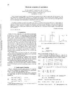
50 nm
b)
a)
c)
Figure 1: XTEM image of an SiO/SiO2 superlattice a) as deposited and b) after annealing at 1100◦ C. For comparison a SiO bulk layer annealed at 1100◦ C is shown (c).
RESULTS By comparison of the XTEM image of the as prepared sample (Fig. 1a) and the at 1100◦ C annealed sample (Fig. 1b) the phase separation of the ultra thin SiO layers (dark) into SiO2 and Si nanocrystals (dark) is clearly visible. The SiO layers of this sample were chosen to be 3 nm. The mean radius of the Si nanocrystals is 3.5 nm±0.5 nm. Fig. 1c shows a SiO bulk layer after the same annealing procedure. The advantages of SiO/SiO2 superlattices in nc-Si size, position and density control are obvious compared to the bulk layer. Please note, that the applied Fresnel defocus method creates contrast between regions of different inner potential in a TEM sample. The appearance of nanocrystals for annealing temperatures of 1100◦ C could be proven by high resolution TEM images and X-ray diffraction measurements on the same samples [17]. S i-O -Si asym m e tric stretching mode 1080 cm
-1
10
5
1000°C
1100 1000 900 800 700 600 500 400 300
1100°C
S L ( 4 n m /3nm )
T ann (°C)
PL intensity [a.u.]
infrared absorption [a.u.]
SL (2nm/3nm)
(560nm ) 300°C
10
400°C
4
500°C
(752nm )
600°C 100°C
(880nm )
900°C
10
1039 -1 cm
3
100 800
900
1000
1100
1200
1300
450
-1
wavenumber [cm ]
a)
600
750
900
1050
w a v e length [nm ]
b)
Figure 2: Temperature dependent FTIR measurements on a SiO/SiO2 superlattice with initially 2 nm thick SiO layers (a) and PL measurements on a sample with 4 nm thick SiO layers (b) [16].
F1.6.4
0.1
1
7
size [nm]
Figure 3: Dependence of confinement energy measured at 5 K on Si crystal size measured by XRD. The solid line shows a theoretical fit assuming a D−0.8 dependence of Ec [21].
5
1.0
4
0.9
3
0.8
2
0.7
1
0.6
0
0.5 10
norm. PL intensity
τ [ms]
confinement energy [eV]
0.6
100
T [K]
Figure 4: Temperature dependence of PL intensity and lifetime for the sample with initially 4 nm thick SiO layer [21].
Annealing experiments using the superlattices samples were performed to reveal the different states of phase separation by comparison of luminescence and infrared characteristics of different samples [16]. The infrared spectra are shown in Fig. 2a) for the sample with 2 nm thickness of the SiO layers and annealing temperatures ranging from 100◦ C (as-prepared) to 1100◦ C. Various silicon-oxygen related absorption bands can be seen in the range from 750 to 1300 cm−1 . The band around 810 cm−1 is assigned to Si-O-Si bond bending motion in SiO2 [20]. With higher annealing temperatures, a band at 880 cm−1 appears and increases in intensity for temperatures of 400-500◦ C. The 880 cm−1 absorption band looses intensity for higher annealing temperature and vanishes above 700◦ C. The IR vibration above 1000 cm−1 is the asymmetric stretching motion of oxygen in a Si-O-Si bridging configuration. The observed IR vibration shifts from 1039 cm−1 to 1052 cm−1 for annealing from 100 to 600◦ C (2.6 cm−1 /100K). Annealing between 700 and 900◦ C results in a more pronounced shift (9.3 cm−1 /100K) with a final position at 1080 cm−1 representing the position found for bulk amorphous SiO2 films [16]. Annealing at higher temperatures does not shift the peak position of the vibration mode further. Fig. 2b) demonstrates the PL spectra at different annealing stages for the sample with 4 nm thick SiO layers. Three different luminescence bands can be distinguished. A band at 560 nm is observed, which increases first in intensity before decreasing again for higher annealing temperatures. At 800◦ C the PL band vanishes in the samples investigated so far. The PL maximum position of this band remains constant independent of the annealing temperature used. At 500◦ C a second luminescence band appears which gradually shifts from a position of 750 nm to 880 nm as the annealing temperature increases from 600◦ C to 900◦ C. The PL intensity of this band is weaker than that of the first luminescence band, but varies from sample to sample. Finally a Gaussian shaped strong luminescence is observed for temperatures above 900◦ C with a peak position clearly depending on the SiO layer thickness, i.e. 900 nm for the sample in Fig. 2b). The intensity of this PL band increases for the 1100◦ C annealing but the peak position remains constant. The PL peak intensity after crystallization is around 10 times stronger then any of the luminescence of the first and second stages. The nc-Si size (D) dependence of the confinement energy (Ec ) for samples annealed at 1100◦ C is shown in Fig. 3 [21]. The crystal size was measured by XRD using the S CHERRER equation and
F1.6.5
agrees with the initial SiO layer thickness of the samples with a variation of about 0.5 nm. Please note that the SiO layer thickness was estimated by scaling down the growth rate measured for a 100 nm thick SiO layer. Ec corresponds to the blueshift of the nc-Si PL band maximum measured at 5 K with respect to the band gap energy of bulk silicon (1.17 eV at 5 K). The exciton binding energy were assumed to be 10 meV. The straight line in Fig. 3 represents a D−0.8±0.1 dependence of Ec . The large error bars for the crystal size measured by XRD are due to the limits of the measurement system given by the very small crystal size and the used overall layer thickness of only about 200 nm for the whole superlattice. Fig. 4 shows the temperature dependence of PL lifetime and PL intensity for temperatures between 300 and 4.5 K. The PL intensity increases with decreasing temperature between 300 K and 200 K. Between 220 K and 70 K the PL intensity does not change significantly and decreases again for temperatures lower than 70 K. The lifetime of the observed luminescence increases for decreasing temperature over the whole measured range from 150 µs at 300 K to 5 ms at 4.5 K. The dependence of the lifetime on Ec measured at a temperature of 100 K is shown in Fig. 5. A clearly decreasing lifetime with increasing confinement energy is observed. Fig. 6 shows a set of resonantly excited PL spectra for different excitation energies (Eex ) indicated by arrows measured on a crystallized sample with an SiO layer thickness of 4 nm [21]. With decreasing excitation energy a structure in the PL spectra becomes more pronounced. Spacing of spectral features with respect to Eex coincides with the energies of momentum-conserving TO (56 meV) or TA phonons (19 meV) of Si or a combination of both. The resonantly excited PL signal divided by the PL signal excited at low laser power in the UV results in a step like function. Each step represents another combination of no-phonon (NP) and phonon-assisted processes in the absorption-emission cycle [22]. By this method the relative transition probability for NP, TO or TA phonon assisted processes can be calculated. The ratio of the NP to phonon-assisted processes determined by the described fitting procedure is plotted versus Ec in Fig. 7. As can be seen here, a significant increase of the relative NP transition probability with increasing Ec is observed. The ratio of NP process probability to the probability
350
PL intensity [a.u.]
1
τ [µs]
300 250 200
0.1
150 0.01
100 0.3
0.4
0.5
0.6
0.7
0.8
0.9
Ec [eV]
Figure 5: Lifetime measured at 100 K depending on Ec [21].
1.3
1.4
1.5
1.6
1.7
Energy [eV]
Figure 6: Resonant excited PL signal for different excitation energies (indicated by arrows) for the samples with 4 nm SiO layer thickness after crystallization [21].
NP / phonon assisted processes
F1.6.6
Figure 7: Ratio of NP to TO phonon assisted processes (triangles) and TA phonon assisted processes (squares) depending on Ec . The solid line is a theoretical fit assuming a E1.7 c dependence of the increasing ratio of NP to TO phonon assisted processes [21].
1 0.32 0.34 0.36 0.38 0.40 0.42 0.44 0.46 0.48
Ec [eV]
of TO phonon assisted process was fitted and scales with E1.7 c represented by a solid line in Fig. 7. Measurements on Er doped nc-Si are shown in Fig. 8 and Fig. 9. Fig. 8 shows the PL intensities of the Si and Er luminescence depending on the Er dose. The Er luminescence of both Er doped nc-Si and bulk SiO2 layer, increases in intensity with increasing Er dose and saturates at a certain dose. The saturation dose for the doped nc-Si is 2×1015 cm−2 and for the doped SiO2 layer 1 × 1016 cm−2 . The Er doped nc-Si show a much stronger luminescence intensity than the doped SiO2 bulk layer. For a dose of 5×1014 cm−2 an enhancement factor of 5000 is observed. The Si luminescence intensity decreases continuously with increasing Er dose.
1.0
50
40
0.6
τ [µs]
PL intensity [a.u.]
0.8
0.4
30
20 0.2 10
0.0 1E14
1E15
1E16 -2
Er dose [cm ]
Figure 8: Comparison of Er implantation dose dependence of the Er3+ luminescence intensity of Er doped nc-Si (•) and bulk SiO2 layers (N). At the same plot the decrease of the nc-Si luminescence intensity with increasing Er dose is shown (�). The maximal Er and Si luminescence intensity are normalized.
0.35
0.40
0.45
0.50
0.55
0.60
Ec [eV]
Figure 9: Ec dependence of the luminescence lifetime of undoped (•) and Er doped nc-Si (�). The nc-Si to Er3+ transfer time (N), estimated as described in the text, decreases clearly for increasing Ec . The Er dose was 2×1015 cm−2 .
F1.6.7
In Fig. 9 the lifetime of the Si luminescence measured at room temperature for Er doped (2×10¹⁵ Er ions/cm2 ) and undoped nc-Si is plotted over Ec . A decrease of the measured lifetime for a doped sample compared to an undoped sample was found over the whole energy range. The measured lifetime (τ ) is a combination of radiative (τr ) and non-radiative lifetimes (τnr ): 1 1 1 = + . τ τr τnr
(1)
Assuming the energy transfer from nc-Si to Er as additional non-radiative channel for the doped sample compared to an undoped sample the measured lifetime can be expressed by: 1 1 1 1 = + + , τ τr τnr τtr
(2)
with τtr denoting the transfer time of the energy transfer of nc-Si to Er3+ . This energy transfer time can then be estimated by comparing the lifetimes of doped and undoped nc-Si. All three, the lifetime of doped and undoped nc-Si and the transfer time decrease for increasing Ec as shown in Fig 9. The lifetime of the Er3+ luminescence was measured to be 2 ms for this sample. DISCUSSION Phase separation The phase separation of SiO into SiOx and Si is already a well known phenomenon [11] and can be expressed by the equation: � x x� SiOx → SiO2 + 1 − Si. (3) 2 2 The combined annealing temperature dependent PL and FTIR measurements revealed three different stages of this phase separation in the limit of ultrathin layers [16]: • Stage 1 for annealing temperatures up to 600◦ C is characterized by a PL signal at 560 nm and a corresponding 880 cm−1 IR absorption. • Stage 2 for annealing temperatures between 600◦ C and 900◦ C still represents an amorphous state of the superlattice. Stage 2 is characterized by a more pronounced IR shift of the Si–O–Si bridging mode above 1000 cm−1 , the vanishing of the PL at 560 nm and the development of a new PL band which gradually shifts its position from 600 nm to 900 nm with increasing temperature. • Stage 3 is observed for annealing temperatures above 900◦ C. It is associated with a very strong red or near infrared luminescence with the peak position depending on the SiO layer thickness, no further changes in the Si-O related absorption band, and Si nanocrystals are detected in the former SiO layer. Stage 1 can be understood as a first rearranging and ordering in bond angles and bond length in the amorphous material without a significant phase separation. The 880 cm−1 absorption mode has been discussed in literature either as a mode related to oxide isolated Si rings [23, 24] or as a
F1.6.8
bending motion of pyramidal oxygen complex [25]. The mode is exclusively observed in the temperature range where reordering takes place and is obviously a signature of such processes. The reconstruction, ordering and phase separation is accompanied by diffusion of Si, O atoms or Si-O groups. The O3 pyramidal configuration discussed in [25] with one oxygen bonded to three silicon atoms seems energetically rather unlikely even for oxygen at the surface of very small Si clusters. Oxide isolated Si rings represent a plane arrangement of the basic lattice cells for the developing Si clusters and Si nanocrystals. It is not clear up to now if there are special groups favoured which mediate the phase separation and diffusion process in the amorphous SiO and show up in IR. Thus, additional experiments and calculations are needed for unambiguous assignment of the 880 cm−1 mode. Bond structures which occur in the matrix during the annealing representing different types of defects as intermediate states could be another explanation for the described IR absorbtion. The to the IR absorption correlated increase and decrease of the defect related PL at 560 nm is a hint for the occurrence of such states. Various explanations for the origin of the 560 nm PL can be found in literature. Rinnert et al. [26] reported an increasing number of radiative defects produced by ion implantation. Jeong et al. [27] suggested that the orange luminescence presumably originates from defects such as the non-bridging oxygen hole center (NBOHC, O3 ≡Si-O•). Also, a decrease of the 560 nm PL intensity and a corresponding decrease of the 880 cm−1 IR absorption is observed in this report above annealing temperatures of 500◦ C. In stage 2 both 560 nm PL band and 880 cm−1 FTIR signal vanishes and a more pronounced IR shift of the Si-O- Si bridging mode above 1000 cm−1 is observed. The peak position can be used for a crude estimate of stoichiometry for homogeneous SiOx [28]. For the bulk SiOx film with x≈1 a position of 980 cm−1 was measured. For the as-prepared superlattice films (100◦ C) a position of 1039 cm−1 was found which is the contribution of both the thin SiO and SiO2 layers. However, a deconvolution of the modes into the SiO and SiO2 parts can not be accomplished in a simple way. Due to the large number of SiO2 interfaces and the very thin layers neither the ¨ effective medium nor the B R UGGEMAN theory is valid for the superlattice system. Hence, the shift of the mode is only a qualitative measure for the progression of the phase separation. The phase separation and the appearance of amorphous Si nanoclusters in the TEM image for annealing temperatures above 600◦ C [16] corresponds to the appearance of the second PL band in stage 2. Similar PL spectra for amorphous Si/SiO2 superlattices prepared by rf magnetron reactive sputtering from a silicon target in argon gas were reported by Liu et al. [29]. Furukawa et al. [30] observed the process of Si cluster formation in SiO2 films for annealing between 750 and 950◦ C. Kanzawa et al. [31] prepared samples by RF co-sputtering of Si and SiO2 which showed a broad PL band in the visible region (1.6-1.9 eV) and a red shift with increasing annealing temperature and Si concentration. This redshift agrees with the redshift shown in Fig. 2b) and corresponds to an increasing size of the amorphous cluster shown by TEM between 600◦ C and 900◦ C [16]. For amorphous clusters the PL signal is expected to be very weak which is in agreement with the shown PL results. Phase 3 is characterized by the presence of nc-Si which leads to a unchanged FTIR signal and the appearance of a very strong PL signal originating from quantum confinement, as will be shown in the next section.
F1.6.9
PL signal of nc-Si A PL signal originating from quantum confinement should show three different properties: a blueshift of the observed PL signal with decreasing crystal size, increasing recombination probability for decreasing crystal size and increasing NP transition probability for decreasing crystal size. A blueshift of the PL signal with decreasing crystal size was shown already for a large variety of nc-Si samples and a D−1.3 dependence of Ec is expected from theoretical calculations [32, 33]. This could experimentally be proven for porous Si [22] as well as for nc-Si produced by LECBD [34]. For the materials system described in this work a D−0.8 dependence of Ec is demonstrated (see Fig. 3) which differ quantitatively from former results for nc-Si, but shows qualitatively the same trend. The recombination probability of an optically active process is inversely proportional to the radiative lifetime. The measured lifetime is a combination of radiative and non-radiative lifetime as described in equation (1). If the temperature dependence of the PL intensity remains constant over a certain temperature range and the lifetime varies as for the investigated samples between 70 and 200 K (see Fig. 4), the measured lifetime is equal to the radiative lifetime. A still existing nonradiative recombination channel would result in a variation of the PL intensity for a temperature dependent lifetime, because the ratio between radiative and nonradiative processes would be changed. Therefore, the decreasing lifetime with increasing Ec at 100 K (see Fig. 5) corresponds to an increasing recombination probability for decreasing crystal size. The appearance of Si phonon-related structures in the resonantly excited PL signal (see Fig. 6) already proves a band to band recombination in nc-Si to be the origin of the shown PL signal. The increasing NP transition probability compared to phonon assisted processes (see Fig. 7) is in agreement with the quantum confinement model. In both cases, NP compared to TO and TA phonon-assisted processes, a relative increase of NP transitions with increasing Ec is observed. −0.8 The transition probability scales with E1.7 c (see fit). Taking into account that Ec scales as D (see Fig. 3) and that phonon-assisted processes scales with the volume of the nc-Si as (1/D)3 [22], one can calculate that the NP recombination probability scales as (1/D)4.4 . Theoretically a (1/D)6 dependence of NP transition probability was calculated [35] and experimentally proven for porous Si [22]. Qualitatively, the PL signal is clearly assigned to quantum confined band to band electron hole recombination in the nc-Si. Even if the calculation of the absolute values of the size dependence of Ec and of the NP transition probability are rather difficult and for the fits shown a number of assumptions had to be made, a reduced size dependence compared to similar systems and theoretical calculations can be assumed. On the other hand, very high absolute values of NP transition for the same Ec value are observed on our samples compared with porous Si [22]. A possible explanation for these phenomena could be a lower effective barrier height due to stoichiometry fluctuations and imperfections in the SiO2 matrix compared to implanted, thermally grown SiO2 , porous Si or nc-Si produced by LECBD. Especially in the last two cases the vacuum level as a barrier for the exciton confined within the nc-Si can be assumed to be infinite. Also the enhanced absolute value of NP transition for the same Ec values could be explained in this way. A lower SiO2 barrier would lead to a smearing out of the electron wave function into the oxide. In this case, a NP transition is more likely due to the amorphous structure of the SiO2 . Tunneling between the nc-Si within one layer can not explain the observed effects, because the
F1.6.10
measurements were done at 4.5 K. Due to the size distribution of the nc-Si only a thermally activated tunneling would be possible which can be neglected for the used low temperatures. Er doping of nc-Si Examples for the role of nc-Si as a sensitizer of the Er3+ luminescence can be found in literature [18, 19, 36]. The mechanism of the energy transfer from nc-Si to the Er3+ ions is still under discussion, even if Watanabe et al. [36] could demonstrate resonant pumping of the Er3+ by the nc-Si by the appearence of dips in the Si luminescence related Er3+ energy levels. The strong enhancement by a factor of 5000 shown in Fig. 8 for the doped nc-Si superlattices compared to doped bulk SiO2 layers clearly indicates the occurrence of an energy transfer from nc-Si to the Er3+ ions. The shortening of lifetime of the nc-Si luminescence by Er doping is surely caused by a combination of the energy transfer between nc-Si and Er3+ and beam damage, but the tendency of shortening of the so called transfer time with increasing Ec (see Fig. 9) can not be explained by beam damage and has to be a property of the energy transfer. The decreasing transfer time corresponds to an increasing transition probability for the nc-Si to Er3+ energy transfer and show the same tendency like the recombination probability within the nc-Si itself (see Fig. 5). This indicates the role of nc-Si as sensitizer for the Er3+ luminescence and was also shown by Watanabe et al. [36], too. An increasing recombination probability of the sensitizer leads to a more efficient pumping of the Er3+ luminescence. The saturation of the enhanced Er3+ luminescence at a Er dose of 2×1015 cm−2 shows that a pumping of more than one Er3+ ion by one nc-Si is possible. Assuming a crystal density of 1019 cm−3 [15] the saturation dose corresponds to a Si nanocrystal to Er3+ ratio which is in the same range as the ratio of Er3+ luminescence lifetime to the transfer time. This ratio should give the maximal number of pumped Er3+ ion per Si nanocrystal. A clustering of the Er cannot be the reason for the described saturation behaviour as can be concluded by the saturation behaviour of the doped bulk SiO2 layers, which saturate in PL intensity only at a dose of 1 × 1016 cm−2 . CONCLUSION A well controlled way of nc-Si synthesis has been demonstrated. The SiO/SiO2 superlattice approach allows an independent control of Si crystal size, depth and density. This well controlled synthesis opens a wide range of applications, but also gives a deeper understanding of the material system. Combined PL and FTIR investigations on the phase separation showed that the different and seemingly contradicting observations in the literature can be understood as different stages of network reorganization. The amorphous state of the SiO layer can be understood as a mixture of Si rings isolated by oxide as nucleation sites for small Si clusters in the temperature range between 100◦ C and 600◦ C. Amorphous Si clusters are growing between 600◦ C and 900◦ C and the crystallization of these amorphous Si clusters takes place above 900◦ C. Si rings, amorphous Si clusters and Si nanocrystals are correlated to different states of a non-stoichiometric SiOx matrix having typical signatures in IR absorption and photoluminescence. The size of the resulting Si nanocrystals is predetermined by the SiO layer thickness and the corresponding cluster size. The luminescence signal of the nc-Si is clearly assigned to quantum confined electron hole recombination within the nc-Si. Increasing recombination probability, confinement energy and NP transition probability with decreasing crystal size were shown. The
F1.6.11
size dependence of all described properties indicates a lower effective barrier height of SiO2 matrix compared to similar systems. The quantum confined origin of the strong PL signal and the dependence of all the named properties is a convincing demonstration of the nc-Si size control via the SiO/SiO2 synthesis approach. The properties of the Er doped nc-Si give clear evidence of energy transfer from the nc-Si to the Er3+ ions with a maximal enhancement factor of 5000. The lowering in transfer time with decreasing crystal size once more underlines the need of the synthesis of very dense arrays of small nc-Si. The SiO/SiO2 superlattice approach is a very convenient way to satisfy this demand. ACKNOWLEDGEMENT The authors gratefully acknowledge G. Lenk from Friedrich-Schiller-University Jena for performing the Er ion implantation. This work was financially supported by the Volkswagen Stiftung and German Research Foundation (DFG). [1] [2] [3] [4] [5] [6] [7] [8] [9] [10] [11] [12] [13] [14] [15] [16] [17] [18] [19] [20] [21] [22] [23]
L. T. Canham. Appl. Phys. Lett., 57:1046, 1990. V. Lehmann and U. G¨osele. Appl. Phys. Lett., 58:856, 1991. Y. Kanemitsu. Phys. Rev. B, 49:16845, 1994. T. Shimizu-Iwayama, D.E. Hole, and P.D. Townsend. Nucl. Instr. and Meth. B, 148:980, 1999. G. Ghislotti, B. Nielsen, P. Asoka-Kumar, K.G. Lynn, A. Gambhir, L.F. Di Mauro, and C.E. Bottani. J. Appl. Phys., 79:8660, 1996. M. L. Brongersma, A. Polman, K. S. Min, E. Boer, T. Tambo, and H. A. Atwater. Appl. Phys. Lett., 72:2577, 1998. T. Shimizu Iwayama, D.E. Hole, and I.W. Boyd. J. Phys.: Condens. Matter, 11:6595, 1999. M. Zhu, Y. Han, R. B. Wehrspohn, C. Godet, R. Etemadi, and D. Ballutaud. J. Appl. Phys., 83:5386, 1998. X. Wu, A.M. Bittner, K. Kern, C. Eggs, and S. Veprek. Appl. Phys. Lett., 77:645, 2000. S. Hayashi and K. Yamamoto. J. of Luminescence, 70:352, 1996. U. Kahler and H. Hofmeister. Optical Materials, 17:83, 2001. M. Ehbrecht and F. Huisken. Phys. Rev. B, 59:2975, 1999. J. St. John, J. L. Coffer, Y. Chen, and R. F. Pinizzotto. J. Am. Chem. Soc., 121:1888, 1999. Y. Hirano, F. Sato, N. Saito, M. Abe, S. Miyazaki, and M. Hirose. J. of Non-Crystal. Sol., 266:1004, 2000. M. Zacharias, J. Heitmann, R. Scholz, U. Kahler, M. Schmidt, and J. Bl¨asing. Appl. Phys. Lett., 80:661, 2002. L.Y. Yi, J. Heitmann, M. Schmidt, R. Scholz, and M. Zacharias. Appl. Phys. Lett., 81:4248, 2002. J. Heitmann, M. Schmidt, R. Scholz, and M. Zacharias. J. of Non-Crystal. Sol., 299:1075, 2002. M. Fujii, M. Yoshida, Y. Kanzawa, S. Hayashi, and K. Yamamoto. Appl. Phys. Lett., 71:1198, 1997. P. G. Kik and A. Polman. J. Appl. Phys., 88:1992, 2000. D. V. Tsu, G. Lucovsky, and B. N. Davidson. Phys. Rev. B, 40:1795, 1989. J. Heitmann, D. Kovalev, F. Eichhorn, L. Yi, and M. Zacharias. J. Appl. Phys., submitted for publication. D. Kovalev, H. Heckler1 M. Ben-Chorin, G. Polisski, M. Schwartzkopff, and F. Koch. Phys. Rev. Lett., 81:2803, 1998. M. Zacharias, D. Dimova-Malinovska, and M. Stutzmann. Philosphical Magazine B, 73:799, 1996.
F1.6.12
[24] V. Belot, R. J. P. Corriu, D. Leclerq, P. Lef`evre, P. H. Mutin, and A. Vioux. J. Non-Cryst. Solids, 127:207, 1991. [25] S.Y. Lin. J. Non-Cryst. Solids, 266-269:850, 2000. [26] H. Rinnert, M. Vergnat, G. Marchal, and A. Bruneau. J. Luminescence, 80:445, 1999. [27] J. Y. Jeong, S. Im, Oh. M. S., H. B. Kim, K. H. Chae, C. N. Whang, and J. H. Song. J. Luminescence, 80:285, 1999. [28] F. Stolze, M. Zacharias, S. Schippel, and B. Garke. Solid State Commun., 87:805, 1993. [29] N. N. Liu, J. M. Sun, S. H. Pan, Z. H. Chen, R. P. Wang, W. S. Shi, and X. G. Wang. Superlattices and Microstructure, 28:157, 2000. [30] K. Furukawa, Y. Liu, H. Nakashima, D. Gao, K. Uchino, K. Muraoka, and H. Tsuzuki. J. Appl. Phys., 72:725, 1998. [31] Y Kanzawa, S Hayashi, and K Yamamoto. J. Phys.: Condens. Matter, 8:4823, 1996. [32] C. Delerue, G. Allan, and M. Lannoo. Phys. Rev. B, 48:11024, 1993. [33] J. P. Proot, C. Delerue, and G. Allan. Appl. Phys. Lett., 61:1948, 1992. [34] G. Ledoux, O. Guillois, D. Porterat, C. Reynaud, F. Huisken, B. Kohn, and V. Paillard. Phys. Rev. B, 62:15942, 2000. [35] M. S. Hybertsen. Phys. Rev. Lett., 37:1514, 1994. [36] K. Watanabe, M. Fujii, and S. Hayashi. J. Appl. Phys., 90:4761, 2001.