Thin Solid Films 515 (2007) 3158 – 3163 www.elsevier.com/locate/tsf
Size and microstructure effects on the mechanical behavior of FCC bicrystals by quasicontinuum method F. Sansoz a,⁎, J.F. Molinari b a
School of Engineering, The University of Vermont, 33 Colchester Avenue, Burlington, VT 05405, USA b Department of Mechanical Engineering, Johns Hopkins University, Baltimore, MD 21218, USA Available online 17 February 2006
Abstract The effects of structure and size on the deformation of b110N tilt bicrystals in copper are investigated by concurrent multiscale simulations at zero temperature. In the simulation of eleven grain boundary (GB) structures, a direct relation is shown between structural units and sliding at GBs. We find that GB sliding operates by atom shuffling events localized on one particular type of structural units, which are present in the GB period. When this type of unit is absent, the GB deformation process occurs by migration, or GB-mediated nucleation of partial dislocations with no sliding, depending on the initial GB configuration. The elastic limit causing sliding is found to vary slightly at zero temperature, but no correlation was obtained with the GB energy at equilibrium. Additionally, both modulus of rigidity, and elastic limit remain constant as the bicrystal size varies from 1 nm up to 25 nm. However, differences in the stress relaxation after sliding are observed with respect to the size. © 2006 Elsevier B.V. All rights reserved. Keywords: Grain boundary structure; Grain boundary cohesion; Nanocrystalline materials; Quasicontinuum simulation
1. Introduction The deformation of nanocrystalline thin films has been the subject of intense interest in recent decades because of their unique, superior mechanical properties as compared to their coarse-grained counterparts [1–4]. Molecular dynamics and experimental results have shown that deformation mechanisms in small nanocrystalline structures are governed by several key parameters: the grain size [5–8], the interatomic potential [6,7], the applied stress [6,9], and the nature of the grain boundary (GB) network [10,11]. Due to their significant volume fraction in nano-grained materials, GBs and triple junctions contribute significantly to the deformation process at various grain sizes. For instance, in nanocrystalline Cu, there is evidence of significant dislocation activity by GB-mediated mechanisms in grains larger than 10–15 nm. This is due to the increased slip process, such as the emissions of extended partial dislocations or the formation of mechanical twins, nucleated from defects present in the GB structure [5–7,9,12–17]. For smaller grain size (b 10 nm), intragranular slip activity is hindered in nanoscale copper. At the same time, however, GB sliding, GB mi⁎ Corresponding author. Tel.: +1 802 656 3837; fax: +1 802 656 1929. E-mail address:
[email protected] (F. Sansoz). 0040-6090/$ - see front matter © 2006 Elsevier B.V. All rights reserved. doi:10.1016/j.tsf.2006.01.012
gration, GB self-diffusion, and triple junction cracking have been observed in nano-grained fcc metals [5–8,12,18–20]. The abnormal rate-dependency and superplasticity in nanocrystalline materials is the subject of intense discussions; see for example the review by Ovid'ko [21]. In fact, nanocrystalline ceramic and metallic materials exhibit superplasticity commonly at lower temperatures and faster strain rates than coarse-grained materials. It is paramount to understand these phenomena at low temperatures in order to define the practical utility of nanocrystalline metals. There is however no theoretical explanations to account for this peculiar behavior because GB-mediated processes are thermally activated in conventional polycrystalline materials. For instance, it is well-established that higher temperatures result in higher GB energies, which causes faster GB sliding rates [22]. Yet, the molecular dynamics simulations of Schiotz and co-workers on the deformation of nanocrystalline copper at zero and finite temperatures [19,23] contradict this theory. These authors have shown that GB sliding remains the main deformation mechanism at all grain sizes up to 13 nm, even at zero temperature. This finding suggests that the sliding and migration of interfaces in nanocrystalline metals, where a diffusional explanation is not relevant at zero temperature, may be encouraged by a non-negligible contribution of athermal effects in the deformation process of nanoscale GBs. While the influence
F. Sansoz, J.F. Molinari / Thin Solid Films 515 (2007) 3158–3163
of GB structure on the thermally activated sliding behavior has been well-documented [24–26], it is unclear how GB structure influences GB sliding in the athermal limit. Another important aspect lies in the fundamental understanding of multiscale deformation processes via hierarchical modeling of nanocrystalline metals using atomistic-based continuum models [27–29]. In this approach, nanostructured materials are regarded as composite structures made of a cohesive GB region separating individual single crystalline phases. The cohesion strength of the GB region is assumed uniform and less than the strength of the grain interior. In general, the interface strength is studied by way of testing bicrystals with well-known GB structure. However, the dependence of bicrystal size on interface behavior is not fully understood, particularly in the nanoscale regime. The present study focuses on the effects of microstructure and size on the nanomechanical behavior of copper bicrystals using well-controlled GB configurations. Molecular simulations using the quasicontinuum method are performed to investigate the deformation of nanoscale bicrystals at zero temperature. Section 2 describes the computational procedure associated with this technique. In Section 3, we report on the influence of interface structure on GB deformation behavior, and address the problem of size dependence on the sliding behavior of one particular GB structure. 2. Computational procedure A cell containing a bicrystal with a GB at its center was modeled using a multiscale atomistic technique, the quasicontinuum method [30,31]. The atomic interactions were treated
3159
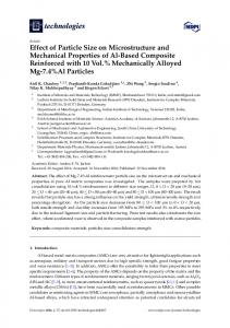
using an embedded-atom-method (EAM) potential for copper [32]. The cutoff distance for this potential is equal to 4.950 Å. The problem was simulated without explicitly representing every atom in the grains. However, atoms near the GB are all represented within a distance from the GB equal to 7.5 times the potential cutoff distance. This is shown in Fig. 1a on the quasicontinuum model of a 25 nm bicrystal containing a Σ9 (221) b110N symmetric tilt GB. This figure also shows that the simulation cell is quasi-planar with only one repeated CSL cell along the tilt vector, c, contained in the GB plane. The ¯ ] direction. The tilt investigated tilt axis was along the [110 angle of the upper and lower grains, referred to as ψ and ψ′ in the following, is defined by the angle between the [110] crystal direction and the normal n of the GB plane. The misorientation angle between the grains is calculated by the sum of ψ and ψ′. Microstructure effects on the mechanical behavior of copper bicrystal have been investigated by the authors in earlier works [31]. The main results of this work are reviewed in Section 3.1 of the present paper. For this type of simulations, the size of the computational cell was kept constant and equal to 11 nm × 39 nm. Here, the aspect ratio of the cell was maintained close to 4 in order to avoid discrepancies due to surface effects. Eleven GB configurations were studied by varying the misorientation angle between the two grains. Two types of tilt GB structure were investigated: symmetric GBs (ψ = ψ′) and asymmetric GBs (ψ ≠ ψ′). In the present paper, size effects were also studied with one particular GB structure promoting GB sliding at zero temperature. The height of the computational cell was varied from 4.4 nm up to 25 nm with a constant aspect ratio of 4. Both 25 nm bicrystal and 4.4 nm bicrystal are shown in Fig. 1a and b, respectively. In this series of simulations, a Σ9(221) b110N
Fig. 1. Quasicontinuum model of copper bicrystals with a GB (bright color atoms) at the center. (a) 25 nm bicrystal. (b) 4.4 nm bicrystal. (c) Boundary conditions for shear loading and crystal definition of the upper and lower grains.
3160
F. Sansoz, J.F. Molinari / Thin Solid Films 515 (2007) 3158–3163
symmetric tilt GB is tested. For the largest bicrystal (25 nm), a mesh adaption technique was used in order to capture the emission of dislocations from the GB to several nanometers within the grain interior. The mesh adaption was triggered when a deformation criterion was reached at the element level. Here, this criterion was reached when the deformation was equal to 0.1. Each cell was initially relaxed under zero force lattice static at zero temperature in order to obtain the lowest state of energy for a given GB configuration. In this process, all atoms in line at the bottom of the lower grain were constrained, thereby avoiding crystal rotation. The energy minimization process was performed using a conjugate gradient method. The total energy was minimized until the addition of out-of-balance forces over the entire system was found less than 10− 3 eV/Å. Because the initial grain shifting may also cause to reach a metastable GB structures, several initial configurations were tested. One of the initial configurations led to the lowest state in energy after atomic relaxation. This procedure is detailed in the following references [31,33]. Only the results obtained for GBs with the lowest state of energy are reported here. Simple homogeneous shear was performed by straining the relaxed bicrystal in a series of incremental shear displacements on the top line of atoms in the upper grain along the n⊗c direction, which is parallel to the GB plane as shown in Fig. 1c. The atoms on the right and left sides of the cell were free of constraints. Between each load step, the strain increment was kept less than 0.15%, and a new energy minimization was performed. The bottom line of atoms in the lower grain was kept fixed in all directions. The top line of atoms in the upper grain is fixed in the n direction. The displacement of all atoms in the simulation cell was constrained along the tilt direction, c. The shear strain γ is given by: g ¼ arctanðd=LÞ In this expression, δ is the imposed shear displacement. L is the size of the unconstrained atomic region. The GB energy was calculated by subtracting the bulk single crystal energy to the bicrystal energy and dividing by the GB area. To limit surface effects in the energy calculation, only 80% of the bicrystal is considered, therefore excluding atoms near free surfaces. The shear stress was calculated by adding the residual forces at the top of the upper grain and dividing by the GB area. Similar to the GB energy calculation, only 80% of the bicrystal was considered in the stress calculation. Despite the approximation made on the stress definition, the authors have shown in earlier works [31,33] that the calculated stress is in excellent agreement with the average stress obtained on molecular dynamics studies of single crystals and bicrystals. In order to detect planar defects and GB structure with respect to the elastically deformed crystal domain, the centrosymmetry parameter proposed by Kelchner et al. [34] was used. We modified the expression proposed by these authors for a quasi2D lattice by calculating the centrosymmetry parameter only on 3 pairs of closest neighbors projected in the tilt plane. In practice, we found that a stacking fault left behind partial
dislocations is detected in Cu when the centrosymmetry parameter is 0.25. For other types of defects i.e., point defects, full dislocations, and free surface atoms, the centrosymmetry parameter is found greater than 0.25. For an elastically deformed crystal, this parameter is zero. The atoms were colored according to the value of the centrosymmetry, appearing in dark color with perfect FCC stacking (centrosymmetry parameter b0.25) and in bright color with crystal defects (centrosymmetry parameter N0.25). 3. Results and discussion 3.1. Effects of microstructure on GB sliding and migration In earlier works [31], the authors have investigated the role of boundary structure on GB-related deformation processes by simulating b110N tilt GB configurations using Al and Cu potentials. Here, in Table 1, we report on eleven copper GB configurations presented in this reference. This table represents for each configuration the elastic limit σmax, the misorientation angle between grains, the Σ value and GB plane orientation, the typical structural units composing the equilibrium GB period (A, B, C, D, E, E′, E″, or A′), and the GB energy at 0 K equilibrium. It is important to point out that the size of the cell used to obtain these results was constant for all GB configurations. The structure of each of the structural units is detailed elsewhere [35]. The 11 GBs were found to deform under shear by 3 distinct deformation mechanisms depending on the GB configuration: GB sliding, GB-mediated partial dislocation nucleation in the absence of GB sliding, and interface migration. GB sliding was manifested by the shuffling of GB atoms when the elastic limit was reached. Atom shuffling events were localized within a small region measuring less than 1 nm in the GB vicinity such that the displacement of few boundary atoms was uncorrelated Table 1 Grain configuration, structure, energetic, elastic limit σmax, and deformation mechanisms of 11 nm copper bicrystals under shear loading Misorientation angle (deg) Deformation by 31.58 20.04 38.94 50.48 39.52
Σ value
(hkl) GB plane
GB sliding: Σ27 (552) Σ33 (441) Σ9 (221) Σ11 (332) Σ121 (110)/(7712)
Energy (mJ/m2)
Structural unit period
σmax (GPa)
870 863 833 699 701
|AEEAEE| |AAEAAE| |EE| |DEDE| |DA′DACDDD… …EDDDACEDD|
2.07 1.90 1.39 1.68 1.55
Deformation by 39.52 59.00 129.52
GB-mediated partial dislocation emissions: Σ11 (225)/(441) 680 |CDCDA′| Σ33 (554) 488 |DDDE″DDDE″| Σ11 (113) 309 |CC|
3.08 1.61 5.41
Deformation by 148.4 13.44 70.52
GB migration: Σ27 (115) Σ73 (661) Σ3 (111)
2.96 1.03 2.35
Results reported in reference [30].
699 674 9
|CBA| |A′A′E′A′A′| |D|
F. Sansoz, J.F. Molinari / Thin Solid Films 515 (2007) 3158–3163
3161
Fig. 2. Deformation of a 25 nm bicrystal under 4.5% shear strain.
to the displacement of the atoms in the upper and lower grains. Subsequently, certain configurations were found to nucleate partial dislocations from the GB to the grain interior from sites showing significant shuffling. This dislocation nucleation process was also observed in the absence of GB atom shuffling for some boundaries as indicated in Table 1 (second mechanism). The third mechanism corresponds to the GB migration by collective motion of interface atoms in a sudden, but correlated manner. The crystal lattice remained dislocation-free during this process. We have observed a direct relation between structural units and onset of sliding at GBs in copper. Table 1 shows that the period of GBs deforming by sliding mechanism is characterized by the presence of structural units of type E. We have also observed that atom shuffling events causing sliding are initiated from this unit. While a high GB energy seems important to predict GB sliding, the above results show that the GB energy is not a sufficient parameter when no thermal activation operates. For instance, the Σ11(332) symmetric tilt GB and Σ27(115) symmetric tilt GB have same GB energy (699 mJ/m2), but only the former promotes GB sliding. The period of the Σ11(332) symmetric tilt GB is made of two E structural units, whereas Σ27 (115) symmetric tilt GB does not contain a single E structural unit. This result is also substantiated in asymmetric tilt configurations such as the Σ121(110)/(7712) GB. Furthermore, it can be seen in Table 1 that σmax varies slightly at zero temperature for the GB sliding mode of deformation. However, there is no correlation of this value with respect to the energy and equilibrium structure of the GBs. For the GBs exhibiting migration under applied strain, we found that σmax varies strongly from one configuration to the other. It is important to note that even at zero temperature, it is possible to find a GB structure migrating at a stress level smaller than the average stress level causing GB sliding. For example, the Σ73 (661) symmetric tilt GB was found to migrate at a stress value of 1.03 GPa. 3.2. Size effects on GB sliding behavior in the athermal limit Particular attention is placed in this section on the evolution of the constitutive parameters in relation to the bicrystal size.
We consider the following constitutive parameters for a bicrystal under shear: the modulus of rigidity G, the elastic limit after the build-up of elastic stresses in the bicrystal σmax, and the variation of stress after sliding of the boundary, Δσ. The size dependence on the mechanical response of a GB was investigated on one of the GBs promoting sliding at zero temperature e.g. a Σ9(221) symmetric tilt boundary. This GB structure was tested in shear using several computational cells with height ranging from only 4.4 up to 25 nm. The shear of a 25 nm Σ9(221) bicrystal at 4.5% strain is represented in Fig. 2. This figure shows that one partial dislocation was nucleated near the center of the boundary and propagated to the grain interior. In fact, the nucleation process was preceded by the atomic shuffling of the boundary at a strain of 2.5% and a stress of 1.30 GPa. This process caused boundary sliding before the partial dislocation nucleation. These results are consistent with the data presented in Table 1 for the same boundary on an 11 nm bicrystal, but in the latter case the value of the stress relaxation after sliding was found more significant.
Fig. 3. Evolution of the shear stress as a function of applied shear strain for bicrystals containing a Σ9(221) b110N symmetric tilt GB with height equal to: 4.4, 11, and 25 nm. Note that the aspect ratio of the computational cell is constant. The shear modulus G, elastic limit σmax and the drop of stress after GB sliding Δσ are also indicated in the insert table for the three sizes. In this table, the unit of size is in nm, while G, σmax and Δσ are given in GPa.
3162
F. Sansoz, J.F. Molinari / Thin Solid Films 515 (2007) 3158–3163
the GB. This indicates that GB atom shuffling has a strong impact on the GB strength. However, for geometries larger than 1 nm, the elastic limit of the bicrystal remains almost constant. It is also worth emphasizing that in the present study, dislocations emitted from the GB were observed for crystals as small as a few nanometers. 4. Conclusions
Fig. 4. Size effects on the GB sliding strength of a Σ9(221) symmetric b110N tilt GB in Cu. The maximum strength of the GB is the strength leading to ideal cleavage at GB i.e. with no GB shuffling or dislocation nucleation. The critical size, at which dislocations start being nucleated from the GB, is also indicated.
In order to understand this difference, we compare in Fig. 3 the stress–strain curves of Σ9(221) bicrystals under shear, for 3 different sizes (4.4, 11 and 25 nm). This figure shows that, as the bicrystal size increases from 4.4 to 25 nm, both modulus of rigidity, and elastic limit σmax remain constant, i.e., 45–50 and 1.3–1.4 GPa, respectively. It is possible to note a slightly lower value of the modulus of rigidity for the 4.4 nm bicrystal. This result is consistent with the size reduction of the crystalline domain in smaller volumes as compared to the more compliant GB region. Fig. 3 also shows that the magnitude of the stress relaxation Δσ after sliding is less significant as the size increases. It is evident that limited stress relaxation occurs after sliding at 2.5% strain in the 25 nm bicrystal. This effect can be interpreted by the fact that in the 4.4 nm bicrystal all dislocations nucleated at the interface were rapidly absorbed by a free surface, while dislocations nucleated in the 25 nm bicrystal never reach the free surfaces for the same level of strain, as shown in Fig. 2. We may therefore suggest that dislocations emission/ absorption at GBs in nano-grained materials are linked to a strong relaxation mechanism, which correlates with the grain size. Our results imply that such repair mechanism may be prevented as the grain size increases. Further efforts in this direction may provide useful insights on the slip process in nanocrystalline materials. We compare in Fig. 4 the evolution of the GB sliding strength as a function of the size using both the data obtained in this study and those referenced in [33]. It is important to note that in reference [33], the aspect ratio of the computational cell was slightly larger, and the height was varied from only few atom planes parallel to the GB up to 6.5 nm. Only shear loading conditions are represented in this figure. The figure shows that the GB strength decreases up to 70% and converges as the size of the bicrystal is increased. The loss of GB strength in this figure is accompanied by a change of deformation mechanism from quasi-cleavage fracture to GB atom shuffling process and, subsequently, to atom shuffling plus dislocation nucleation from
A series of multiscale simulations have been performed to assess the influence of structure and size on the sliding behavior of nanocrystalline tilt GBs. The following conclusions can be drawn from this investigation: (1) a direct relation exists between structure and sliding at GBs in the athermal limit; here, GB sliding is only found in interfaces containing E structural units; (2) the equilibrium GB energy is not a sufficient parameter to predict the onset of GB sliding when no thermal activation operates, (3) the elastic limit causing sliding varies slightly at zero temperature, but with no apparent correlation to the equilibrium GB energy; (4) there is a size dependence on the stress relaxation after sliding at GBs; and (5) size effects on the sliding strength and elasticity of nanoscale GBs are limited in bicrystals larger than 1 nm. These findings provide additional insights for deformation of nanocrystalline metallic thin films at low temperatures. Acknowledgments This work was performed under the auspices of NSFNanoscale Interdisciplinary Research Team under contract DMR-0210215 and ARL-Center for Advanced Materials and Ceramic Systems under the ARMAC-RTP Cooperative Agreement Number DAAD19-01-2-0003. FS would like to acknowledge support from NSF-Vermont Experimental Program to Stimulate Competitive Research (VT EPSCoR) under grant number NSF EPS 0236976. References [1] R.W. Balluffi, A.P. Sutton, Mater. Sci. Forum 207–209 (1996) 1. [2] J.R. Weertman, D. Farkas, K. Hemker, H. Kung, M. Mayo, R. Mitra, H. Van Swygenhoven, MRS Bull. (1999 February) 44. [3] A. Robertson, U. Erb, G. Palumbo, Nanostruct. Mater. 12 (1999) 1035. [4] K.S. Kumar, H. Van Swygenhoven, S. Suresh, Acta Mater. 51 (2003) 5743. [5] J. Schiotz, K.W. Jacobsen, Science 301 (2003) 1357. [6] V. Yamakov, D. Wolf, S.R. Phillpot, A.K. Mukherjee, H. Gleiter, Nature Mater. 3 (2004) 43. [7] H. Van Swygenhoven, P.M. Derlet, A.G. Froseth, Nature Mater. 3 (2004) 399. [8] A.C. Lund, T.G. Nieh, C.A. Schuh, Phys. Rev. B 69 (2004) 012101. [9] V. Yamakov, D. Wolf, M. Salazar, S.R. Phillpot, H. Gleiter, Acta Mater. 49 (2001) 2713. [10] H. Van Swygenhoven, M. Spaczer, A. Caro, Nanostruct. Mater. 10 (1998) 819. [11] H. Van Swygenhoven, A. Caro, D. Farkas, Mater. Sci. Eng., A 309–310 (2001) 440. [12] Z. Shan, E.A. Stach, J.M.K. Wiezorek, J.A. Knapp, D.M. Follstaedt, S.X. Mao, Science 305 (2004) 654. [13] X.Z. Liao, F. Zhou, E.J. Lavernia, S.G. Srinivasan, M.I. Baskes, D.W. He, Y.T. Zhu, Appl. Phys. Lett. 83 (2003) 632. [14] V. Yamakov, D. Wolf, S.R. Phillpot, H. Gleiter, Acta Mater. 50 (2002) 5005.
F. Sansoz, J.F. Molinari / Thin Solid Films 515 (2007) 3158–3163 [15] M. Chen, E. Ma, K.J. Hemker, Y.M. Wang, X. Cheng, Science 300 (2003) 1275. [16] H. Rosner, J. Markmann, J. Weissmuller, Philos. Mag. Lett. 84 (2004) 321. [17] X.Z. Liao, F. Zhou, E.J. Lavernia, D.W. He, Y.T. Zhu, Appl. Phys. Lett. 83 (2003) 5062. [18] J. Schiotz, T. Rasmussen, K.W. Jacobsen, Philos. Mag. A 74 (1996) 339. [19] J. Schiotz, F.D. Di Tolla, K.W. Jacobsen, Nature 391 (1998) 561. [20] I.A. Ovid'ko, A.G. Sheirnerman, Acta Mater. 52 (2004) 1201. [21] I.A. Ovid'ko, Int. Mater. Rev. 50 (2005) 1. [22] A.P. Sutton, R.W. Balluffi, Interfaces in Crystalline Materials, Clarendon Press, Oxford, UK, 1995. [23] J. Schiotz, T. Vegge, F.D. Di Tolla, K.W. Jacobsen, Phys. Rev. B 60 (1999) 11971. [24] N. Chandra, P. Dang, J. Mater. Sci. 34 (1999) 655. [25] S. Namilae, N. Chandra, T.G. Nieh, Scripta. Mater. 46 (2002) 49.
[26] [27] [28] [29]
[30] [31] [32] [33] [34] [35]
3163
R.A. Hoagland, R.J. Kurtz, Philos. Mag. A 82 (2002) 1073. Y.J. Wei, L. Anand, J. Mech. Phys. Solids 52 (2004) 2587. H.H. Fu, D.J. Benson, M.A. Meyers, Acta Mater. 52 (2004) 4413. D.H. Warner, F. Sansoz, J.F. Molinari, in: I. Ovid'ko, C.S. Pande, R. Krishnamoorti, E. Lavernia, G. Skandan (Eds.), Mechanical Properties of Nanostructured Materials and Nanocomposites, Boston, MA, December 1–5, 2003, Materials Research Society Symposium Proceeding, vol. 791, 2004, Q5.31.1. R. Miller, E. Tadmor, J. Comput.-Aided Mater. Des. 9 (2002) 203. F. Sansoz, J.F. Molinari, Acta Mater. 53 (2005) 1931. S.M. Foiles, M.I. Baskes, M.S. Daw, Phys. Rev. B 33 (1986) 7983. F. Sansoz, J.F. Molinari, Scripta. Mater. 50 (2004) 1283. C.L. Kelchner, S.J. Plimpton, J.C. Hamilton, Phys. Rev. B 58 (1998) 11085. J.D. Rittner, D.N. Seidman, Phys. Rev. B 54 (1996) 6999.