Here, we investigate the size effect of perpendicular-anisotropic double-barrier magnetic tunnel junction (MTJ) devices embedded with iron nanoparticles.
IEEE TRANSACTIONS ON MAGNETICS, VOL. 51, NO. 11, NOVEMBER 2015
1000704
Size Effect on Interlayer Coupling and Magnetoresistance Oscillation of Magnetic Tunnel Junction Embedded With Iron Nanoparticles Yen-Chi Lee1 , Bipul Das1 , Te-Ho Wu2 , Lance Horng1 , and Jong-Ching Wu1 1 Department
2 Graduate
of Physics, National Changhua University of Education, Changhua 500, Taiwan School of Material Science, National Yunlin University of Science and Technology, Douliu 640, Taiwan
Here, we investigate the size effect of perpendicular-anisotropic double-barrier magnetic tunnel junction (MTJ) devices embedded with iron nanoparticles. A sputtering system in conjunction with the postannealing process is employed to prepare the sheet film and standard lithography techniques followed by the ion etching technique are used to fabricate the micrometer to submicrometer MTJ devices. A strong ferromagnetic coupling is observed as we reduce the size of the device to submicrometer scale, which is due to the reduction of magnetostatic energy of the device. Furthermore, a magnetoresistance (MR) oscillation is observed at room temperature while reducing the size of the device. MR peaks at low bias fields are believed to have magnon contributions, whereas the peaks observed at higher bias fields are responsible for phonon-assisted tunneling. Zero-bias anomalies are also observed and are more prominent in antiparallel states of the devices. Index Terms— Magnetic tunnel junction (MTJ), nanoparticles, perpendicular anisotropy, size effect.
I. I NTRODUCTION AGNETIC tunnel junction (MTJ) is an attractive issue in the field of spintronics due to its potential application in spin diode [1]–[3], magnetic field sensor [4], and nonvolatile spin-transfer-torque magnetic random access memories [5], [6]. In particular, the MTJs with an ultrathin crystalline MgO barrier produce a high tunneling magnetoresistance (TMR) ratio and a low resistance area product [7]–[10] that is adaptable to the present semiconductor integrated circuits [11]. The MR of the MTJs decays upon raising the bias voltage, which limits the operating range of the device. Some reports show that, the devices connected in series configuration would not only resolve this problem but also reduce the noise [12], [13], but the power consumption would be increased proportionally with the total impedance. Recently, the double-barrier (DB) MTJ consisting of two insulating layers alternated by two or three magnetic layers has been employed to resolve this problem. In addition, this DB structure gives rise to a high spin-filtering efficiency thus not only enhancing the TMR ratio [14], but also reducing the critical current density for spin-transfer-torque switching [15] that promotes the performance of spintronics devices. Besides mentioned above, there are many efforts that have been devoted to investigate the bias voltage dependence of the electron transport in DBMTJ at low bias voltages both experimentally and theoretically [16]–[18]. Do obeisance a nanofabrication grant, Coulomb charging effect and quantum-well (QW) effect at relatively higher bias voltages results in the MR oscillation or in the local MR enhancement around few hundred millielectronvolts to millivolts region have
M
Manuscript received March 20, 2015; revised May 22, 2015; accepted May 26, 2015. Date of publication June 1, 2015; date of current version October 22, 2015. Corresponding author: J.-C. Wu (e-mail: phjcwu@ cc.ncue.edu.tw). Color versions of one or more of the figures in this paper are available online at http://ieeexplore.ieee.org. Digital Object Identifier 10.1109/TMAG.2015.2438326
been predicted and observed [19]–[23]. In specific case of a granular insertion layer with magnet, the Kondo-assisted tunneling effect has also been reported [24]. However, it is to say that the tunneling mechanism is still not clearly understood. Comparing to the in-plane anisotropy, the MTJs with perpendicular anisotropy (p-MTJ) have more potential in raising the operating speed and cell density [25]–[27]. But, the p-MTJ with thin MgO barrier is not easy to prepare due to the interfacial conditions, thicknesses of the magnetic layers, and interlayer coupling. Herein, we characterize the p-MTJ with iron nanoparticles insertion and investigate the device size effect on the interlayer coupling and MR behavior. II. E XPERIMENT The stacked film of Ta(25)/Co40Fe40 B20 (1.3)/MgO(1)/ Fe(0.1)/MgO(1)/Co20Fe60 B20 (2.2)/Ta(5) (unit in nanometer) is prepared by an ultrahigh vacuum magnetron sputtering system at the ambient temperature. Sequentially, an annealing process at 300 °C for 1 h in the absence of any external magnetic fields is performed to form a uniform arrangement of iron (Fe) nanoparticles naturally, as shown in [28]. Subsequently, the film is characterized using an alternative gradient magnetometer (AGM) to confirm the anisotropy and switching behavior. An AGM measurement of the film reveals perpendicular anisotropies with two sharp transitions but a slow variation at low field after the first transition, and is shown in Fig. 1(a). Two sharp transitions are the switching of CoFeB layers, and the slow transition is suggested due to the contribution of Fe nanoparticles. The reversal starts with the switching of the free layer (FL) of Co20 Fe60 B20 at lower external magnetic field (H ) and ends with the switching of the reference layer (RL) of Co40 Fe40 B20 at higher magnetic field. The slow transition at the middle is due to the distribution of switching field of individual iron nanoparticles embedded in the device. Standard lithographic techniques in conjunction with ion etching technique [29] are employed to manufacture a series of current-perpendicular-to-plane DB-MTJ devices with the elliptical shaped lateral dimensions of ∼4 μm × 8 μm,
0018-9464 © 2015 IEEE. Personal use is permitted, but republication/redistribution requires IEEE permission. See http://www.ieee.org/publications_standards/publications/rights/index.html for more information.
1000704
IEEE TRANSACTIONS ON MAGNETICS, VOL. 51, NO. 11, NOVEMBER 2015
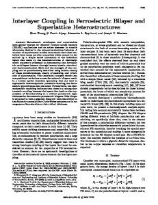
Fig. 1. (a) M–H loop of the sheet film with the magnetization states of different layers are shown by arrows, which indicate the magnetization reversal process. Inset: schematic of a device. The three transitions are corresponding to the three ferromagnetic layers. (b) Major and (c) minor MR versus H loops of the MTJ devices at room temperature.
Fig. 2. Bias-dependent MR behaviors at high (AP)/low (P) states (top panels) and the normalized TMR (bottom panels) of the devices with the dimensions of (a) 4 μm × 8 μm, (b) 1 μm × 2 μm, and (c) 0.3 μm × 0.6 μm, respectively.
1 μm × 2 μm, and 0.3 μm × 0.6 μm. Room temperature MR behaviors of the devices are characterized using dc and a differential resistance measurement. For the differential resistance measurement, the sensing current is 5 nA at 73 Hz frequency and the dc bias range is from −150 to 150 mV. We use SR830 lock-in-amplifier with an input impedance of 10 M�. The resistance of the sample with the dimension of ∼0.3 μm × 0.6 μm is larger than the input impedance. Therefore, the differential resistance behavior of the sample is obtained by the numerical calculation. III. R ESULTS AND D ISCUSSION Fig. 1(b) shows the major MR–H loops of 4 μm × 8 μm (black square), 1 μm × 2 μm (red circle), and 0.3 μm × 0.6 μm (blue triangle), respectively, and all the switching fields are larger than the sheet film. Furthermore, the slow transition at low field just can be observed in the device 4 μm × 8 μm, that is to say the magnetic reversal of the iron nanoparticles is together with one of the CoFeB layers in the smaller devices. The antiparallel (AP) state is getting more unstable and reversals become sharper as the lateral size is reducing, means the coercivity of each ferromagnetic layer
is approaching closer to each other. In addition, we can say that, in order to lower the magnetostatic energy, the system prefers to be in the parallel (P) state. Fig. 1(c) displays the minor MR loops of all the devices, and the AP states cannot be kept without applying a negative magnetic field. This tendency is also the evidence of ferromagnetic coupling among the magnetic layers of the device. Iron nanoparticles, having a finite distribution of particle sizes and individual particle switching fields, greatly influence the interlayer coupling of FL and RL. In larger devices, it makes the AP states easy to achieve and results in a low switching fields, whereas at low dimensions of the device, the less distribution of the particle sizes and their individual switching fields make it hard to get an AP state of RL and FL. At larger dimensions of the devices, both the P and AP states are stable due to higher demagnetization fields along the out-of-plane direction of the devices. On contrary, at smaller device sizes, the AP state becomes unstable due to less demagnetization energy along the out-of-plane direction. Fig. 2 reveals the bias-dependent resistance of AP and P states of each device (top panels) and the bias-dependent normalized TMR behaviors at room temperature (bottom panels).
LEE et al.: SIZE EFFECT ON INTERLAYER COUPLING AND MR OSCILLATION OF MTJ
The largest device (4 μm × 8 μm) shows a typical behavior of decreasing MR values with increase in the bias voltage in both the AP and P states, as shown in Fig. 2(a). However, the device with size of ∼1 μm × 2 μm displays some local enhancement of TMR behavior, as shown in Fig. 2(b). In Fig. 2(c), we see some local variation of resistance with increasing the bias (both negative and positive) voltage results in a significant MR oscillation behavior of the device having the smallest size of ∼0.3 μm × 0.6 μm. To roughly distinguish what cause this MR oscillation, the energy scale can shed a light upon the observed behavior. For the charging effect, the energy level would be of few millivolts and would not be revealed in the symmetrical barrier system, i.e., with the same thickness of each barrier [20]. In addition, a single-electron tunneling predicts an oscillation period (here, it is ∼63.7 mV) of e/C, which gives the C value of ∼37.2 aF, where C is the total capacitance of junctions and e is charge of an electron. But, the geometry of our device with size of ∼0.3 μm × 0.6 μm indicates the C value of ∼0.025 fF, which is obviously incongruous. Consequently, the MR oscillation due to the charging effect can be ruled out as a possible reason. The spin mean free paths of majority and minority spins of iron, which are typically of ∼15 ± 2 Å and 21 ± 5 Å, respectively [30], are comparable with the dimension of the nanoparticles in our system. If we consider the Bloch states with different symmetries, we know that the top of �2 and �5 states of the majority spins are at 0.2 V above the Fermi energy, E F for Fe. For Co, the top of �2 state of the minority spins is at 0.3 V above the E F [8], [31]. Consequently, the energy levels for a QW effect are in the range of a few hundreds of millivolts, far away from our observed results. However, �1 Bloch states are at E F in the bcc crystalline ferromagnetic CoFeB electrodes and can tunnel through the barriers. In addition, the typical magnon peaks and phonon peaks for the symmetrical MgO-based DB-MTJ are within the ranges of ∼40–70 meV and 81–162 meV, respectively [16]–[18]. Therefore, we can say that, the first peaks (at −47.7 mV and at 65.9 mV) observed for both the directions of applied bias voltage are correspond to magnon-assisted tunneling, whereas the second peaks (at −108.3 mV and at 129.2 mV) are correspond to the phonon-assisted tunneling of electrons. If notice carefully, we observe the peaks are present in both P and AP alignments. It is to be noted that no local enhancement of MR is present in the largest device and only reduced phonon peaks are observed in the device size of ∼1 μm × 2 μm. That is to say the phenomena are universal but, a larger distribution of iron nanoparticle size may have smeared out the fine structure of MR oscillations. Asymmetric peaks near zero-bias voltages are observed almost in all the devices, which are more in the AP states, perhaps come from the magnetic impurities present in the devices. A nonuniform magnetization of iron nanoparticles and a nonuniform surface roughness of barrier layers are the sources of magnetic impurities. Now, as the AP states are magnetically more unstable compared with the P states, the magnetic impurities influence more the AP states and make the corresponding MR curves asymmetrical near
1000704
the zero-bias voltages. The observed low MR% in both the AP and P states may be due to less filtering of �1 Bloch states than as expected by the barrier layers. There are other reasons for getting low MR values, such as the nonuniform magnetization of iron nanoparticles and an effective large gap between the uniformly magnetized FL and RL both of which make the electrons coming to the FL to be less polarized. Presence of any pin holes can decrease the MR% even more. IV. C ONCLUSION In summary, the perpendicularly anisotropic MTJs embedded with iron nanoparticles have been prepared and patterned successfully into micrometer and submicrometer scale devices. A size-dependent ferromagnetic coupling has been observed that is suggested due to the reduction of the magnetostatic energy inside the device. Bias-dependent resistances oscillations are present in both the P and AP states of the devices resulting in distinct peaks in TMR oscillations that are correspond to magnon- and phonon-assisted tunneling. The phenomenon of MR oscillation becomes prominent while reducing the size of the devices, which is due to the less size distribution of the iron nanoparticles. A more detailed study of the peaks would be done in the future. ACKNOWLEDGMENT This work was supported by the National Science Council of Taiwan under Grant NSC 101-2112-M-018-004-MY3. R EFERENCES [1] M. Chshiev, D. Stoeffler, A. Vedyayev, and K. Ounadjela, “Magnetic diode effect in double-barrier tunnel junctions,” Europhys. Lett., vol. 58, no. 2, pp. 257–263, 2002. [2] F. Giazotto, F. Taddei, R. Fazio, and F. Beltram, “Ferromagnetic resonant tunneling diodes as spin polarimeters,” Appl. Phys. Lett., vol. 82, no. 15, pp. 2449–2451, 2003. [3] A. Iovan, S. Andersson, Y. G. Naidyuk, A. Vedyaev, B. Dieny, and V. Korenivski, “Spin diode based on Fe/MgO double tunnel junction,” Nano Lett., vol. 8, no. 3, pp. 805–809, 2008. [4] J. M. Almeida, P. Wisniowski, and P. P. Freitas, “Field detection in single and double barrier MgO magnetic tunnel junction sensors,” J. Appl. Phys., vol. 103, no. 7, p. 07E922, 2008. [5] S. Ikegawa et al., “A fully integrated 1 kb magnetoresistive random access memory with a double magnetic tunnel junction,” Jpn. J. Appl. Phys., vol. 42, no. 7A, pp. L745–L747, 2003. [6] T. Uemura, S. Honma, T. Marukame, and M. Yamamoto, “Novel magnetic random access memory cell consisting of magnetic tunnel junction connected in parallel with negative differential resistance device,” Jpn. J. Appl. Phys., vol. 43, no. 4S, p. 2114, 2004. [7] S. Yuasa, T. Nagahama, A. Fukushima, Y. Suzuki, and K. Ando, “Giant room-temperature magnetoresistance in single-crystal Fe/MgO/Fe magnetic tunnel junctions,” Nature Mater., vol. 3, pp. 868–871, Oct. 2004. [8] S. Yuasa and D. D. Djayaprawira, “Giant tunnel magnetoresistance in magnetic tunnel junctions with a crystalline MgO(0 0 1) barrier,” J. Phys. D: Appl. Phys., vol. 40, no. 21, pp. R337–R354, 2007. [9] D. V. Dimitrov, Z. Gao, X. Wang, W. Jung, X. Lou, and O. Heinonen, “Transport properties of MgO magnetic tunnel junctions,” J. Appl. Phys., vol. 105, no. 11, p. 113905, 2009. [10] Q. L. Ma et al., “Temperature dependence of resistance in epitaxial Fe/MgO/Fe magnetic tunnel junctions,” Appl. Phys. Lett., vol. 95, no. 5, p. 052506, 2009. [11] M. Rieth and W. Schommers, Handbook of Theoretical and Computational Nanotechnology, vol. 10. Valencia, CA, USA: Amer. Sci. Pub., 2006, p. 469. [12] F. Montaigne et al., “Enhanced tunnel magnetoresistance at high bias voltage in double-barrier planar junctions,” Appl. Phys. Lett., vol. 73, no. 19, pp. 2829–2831, 1998.
1000704
[13] R. Guerrero, M. Pannetier-Lecoeur, C. Fermon, S. Cardoso, R. Ferreira, and P. P. Freitas, “Low frequency noise in arrays of magnetic tunnel junctions connected in series and parallel,” J. Appl. Phys., vol. 105, no. 11, p. 113922, 2009. [14] A. N. Useinov, J. Kosel, N. K. Useinov, and L. R. Tagirov, “Resonant tunnel magnetoresistance in double-barrier planar magnetic tunnel junctions,” Phys. Rev. B, vol. 84, p. 085424, Aug. 2011. [15] Z. Diao et al., “Spin transfer switching in dual MgO magnetic tunnel junctions,” Appl. Phys. Lett., vol. 90, no. 13, p. 132508, 2007. [16] G.-X. Miao et al., “Inelastic tunneling spectroscopy of magnetic tunnel junctions based on CoFeB/MgO/CoFeB with Mg insertion layer,” J. Appl. Phys., vol. 99, no. 8, p. 08T305, 2006. [17] V. Drewello et al., “Inelastic electron tunneling spectra of MgO-based magnetic tunnel junctions with different electrode designs,” Phys. Rev. B, vol. 79, p. 174417, May 2009. [18] D. L. Li et al., “Tunneling processes in asymmetric double barrier magnetic tunnel junctions with a thin top MgO layer,” J. Appl. Phys., vol. 114, no. 21, p. 213909, 2013. [19] J. Barna´s and A. Fert, “Magnetoresistance oscillations due to charging effects in double ferromagnetic tunnel junctions,” Phys. Rev. Lett., vol. 80, pp. 1058–1061, Feb. 1998. [20] R. Liu et al., “Tunneling magnetoresistance oscillations due to charging effects in MgO double barrier magnetic tunnel junctions,” Appl. Phys. Lett., vol. 100, no. 1, p. 012401, 2012. [21] R. C. Temple and C. H. Marrows, “Single-electron spin interplay for characterization of magnetic double tunnel junctions,” Phys. Rev. B, vol. 88, p. 184415, Nov. 2013. [22] R. S. Liu et al., “CoFe alloy as middle layer for strong spin dependent quantum well resonant tunneling in MgO double barrier magnetic tunnel junctions,” Phys. Rev. B, vol. 87, p. 024411, Jan. 2013.
IEEE TRANSACTIONS ON MAGNETICS, VOL. 51, NO. 11, NOVEMBER 2015
[23] J. M. Teixeira, J. D. Costa, J. Ventura, J. B. Sousa, P. Wisniowski, and P. P. Freitas, “Observation of spin-dependent quantum well resonant tunneling in textured CoFeB layers,” Appl. Phys. Lett., vol. 104, no. 11, p. 112414, 2014. [24] H. Yang, S. H. Yang, and S. S. P. Parkin, “Crossover from Kondo-assisted suppression to co-tunneling enhancement of tunneling magnetoresistance via ferromagnetic nanodots in MgO tunnel barriers,” Nano Lett., vol. 8, no. 1, pp. 340–344, 2008. [25] A. D. Kent, B. Özyilmaz, and E. del Barco, “Spin-transfer-induced precessional magnetization reversal,” Appl. Phys. Lett., vol. 84, no. 19, pp. 3898–3899, 2004. [26] H. Liu, D. Bedau, D. Backes, J. A. Katine, J. Langer, and A. D. Kent, “Ultrafast switching in magnetic tunnel junction based orthogonal spin transfer devices,” Appl. Phys. Lett., vol. 97, no. 24, p. 242510, 2010. [27] M. Nakayama et al., “Spin transfer switching in TbCoFe/CoFeB/MgO/CoFeB/TbCoFe magnetic tunnel junctions with perpendicular magnetic anisotropy,” J. Appl. Phys., vol. 103, no. 7, p. 07A710, 2008. [28] Y.-C. Lee, C.-H. Lin, A. K. Mishra, T.-H. Wu, and J.-C. Wu, “Size effect of inserted iron nanoparticles in the MgO-based double barrier magnetic tunnel junction,” IEEE Trans. Magn., vol. 50, no. 1, Jan. 2014, Art. ID 1401103. [29] H.-M. Lee et al., “The development of perpendicular magnetic tunneling junctions,” Spin, vol. 2, no. 1, p. 1230002, 2012. [30] B. A. Gurney, V. S. Speriosu, J.-P. Nozieres, H. Lefakis, D. R. Wilhoit, and O. U. Need, “Direct measurement of spin-dependent conductionelectron mean free paths in ferromagnetic metals,” Phys. Rev. Lett., vol. 71, pp. 4023–4026, Dec. 1993. [31] J. M. Teixeira et al., “Electrode band structure effects in thin MgO magnetic tunnel junctions,” Appl. Phys. Lett., vol. 100, no. 7, p. 072406, 2012.