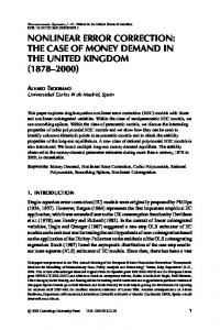
AbstractâIn this paper a soft error correction scheme for embedded storage elements in level sensitive designs is presented. It employs space redundancy to ...
Soft Error Correction in Embedded Storage Elements Michael E. Imhof, Hans-Joachim Wunderlich Institute of Computer Architecture and Computer Engineering University of Stuttgart, Pfaffenwaldring 47, D-70569 Stuttgart, Germany email: {imhof, wu}@iti.uni-stuttgart.de Abstract—In this paper a soft error correction scheme for embedded storage elements in level sensitive designs is presented. It employs space redundancy to detect and locate Single Event Upsets (SEUs). It is able to detect SEUs in registers and employ architectural replay to perform correction with low additional hardware overhead. Together with the proposed bit flipping latch an online correction can be implemented on bit level with a minimal loss of clock cycles. A comparison with other detection and correction schemes shows a significantly lower hardware overhead. Keywords—Single Event Effect, Correction, Latch, Register
I. I NTRODUCTION Transient faults caused by neutron and alpha particle strikes have become the main source for reliability degradation of digital systems. For circuits being composed out of memory and random logic blocks, both parts can experience soft errors [1]. In recent years the combinatorial logic and sequential elements of a typical design contributed about 60% of the overall Soft Error Rate (SER) [2]. In actual technologies random logic can be seen as the main source of soft errors due to two trends: The proliferated use of protection schemes for dedicated memory blocks like SRAMs or caches leads to a significantly reduced contribution to the overall SER. Continued technology scaling and decreasing feature sizes increase the absolute soft error rates for the unprotected random logic. The SER contribution of combinatorial logic is considerably smaller than that of the sequential elements [2, 3] as SETs produced in the combinational logic are filtered by several mechanisms: Transient pulses or glitches are attenuated by the transistors of a gate or happen on off-path inputs (electrical and logical masking). The pulses reaching a latch result only in an error when they are latched (latch window masking). Sequential elements embedded in random logic have the highest potential of sacrificing the overall SER. Single Event Upsets (SEUs) directly affecting a latch can permanently alter the stored value. They are directly visible at the latch output and often affect large portions of a design. Therefore, soft error protection techniques for sequential elements such as latches will contribute most in improving a circuits robustness. Several schemes have been proposed to protect sequential elements in random logic. Space redundancy, first proposed as triple modular redundancy (TMR [4, 5]) and triple latches [6] was later on extended by time redundancy. The correction is performed either by recomputation (RAZORII [7]), restoring the good value from a shadow element (GRAAL, RAZOR, BISER [8–10]) or by information redundancy (Parity or Ham-
ming [11, 12]). Other solutions filter explicitly input signals (DF-DICE [13]). The scheme presented in [12] analyzes the protection of registers with a hamming code, and the authors state a not negligible hardware overhead. The scheme proposed here is also based on a linear code and it is able to detect and correct single event upsets in registers embedded in random logic. Information redundancy is added to all registers and used to detect single event upsets with significantly less hardware costs than what was reported in [12]. The used code is able to localize the affected bit within a register. Using this information to control the developed bit flipping latch corrects the single event upset while loosing one clock cycle. No additional clock cycles are used when no upsets occur and no additional gates have to be inserted in the data path. The presented scheme is composed of the following contributions: 1) Efficient error detecting and correcting (EDAC) code computation: A modulo-2 address characteristic is used to derive a log(n)-bit checksum of the n-bit register content [14]. The characteristic computation is implemented using standard cells, resulting in a low area overhead. 2) Protected storage of the error condition: The properties of the characteristic yield in the detection of a state change together with the localization of the affected bit. An additional parity protection detects soft errors directly altering the stored characteristic. 3) Bit flipping latch: The localized soft error can be corrected with the help of the developed bit flipping latch standard cell. This implies that (i) all single event upsets can be detected and corrected by recomputation with a low hardware overhead. (ii) the computed checksum is effectively protected against SEUs and no unnecessary recomputations (false positives) can happen. (iii) the used code allows a localization of the affected bit. (iv) the localization information can be fed back to the developed bit flipping latches to correct a happened SEU in one additional clock cycle. (v) the time vulnerability factor is very low. (vi) the overall scheme results in a low hardware overhead. The rest of this paper is organized as follows: Section II discusses the related work for soft error detection and correction while section III discusses the basic ideas of the proposed scheme. Section IV depicts the area efficient implementation
III. P ROPOSED C ORRECTION F LOW
II
1-out-of-n Decoder
n
n
a) Unprotected
Fig. 1.
n
log(n)
n
n
b) Detection and Recomputation
...
n
fail
log(n) latches
III
n bit flipping latches
fail
log(n) latches
Let figure 1-a be a unprotected register composed of n latches. Figure 1-b depicts an abstract view on the proposed detection of SEUs when the correction can be performed using recomputation. The register is complemented with the proposed area efficient modulo-2 address characteristic computation. The reference characteristic is stored in log(n) additional latches. It is then compared to the current characteristic. If a difference is detected the f ail signal is raised and triggers the recomputation.
...
Due to the non regular structure and the composition of random logic most protection schemes introduce local space redundancy for each bit. Working at bit level makes correction feasible but limits the reachable efficiency in terms of achievable hardware overhead. The most prominent schemes include BISER, DF-DICE, RAZOR and GRAAL [8–10, 13]. Triple modular redundancy [4, 5] describes the composition of a reliable system out of unreliable components. The basic building blocks get triplicated and their results are combined using a synchronous majority voter. Triple latches extend TMR by time redundancy and an asynchronous voter to improve the detection probability [6]. Triplication is able to correct all single bit upsets. The hardware overhead of around +400% (two latches plus voter) can be reduced by different techniques. The BISER scheme [2] combines one latch and the voter of TMR into an asynchronous majority voter, the C-Element. If the register is scanable, the scan portion can be reused to implement one of the two remaining latches. BISER is able to detect single bit upsets and hinders them from propagating to the output using the voter. The GRAAL scheme proposed by Nicolaidis is based on space and time redundancy [8] and was proposed for a level-sensitive design style. The value of a redundant sequential element is compared to the value of the functional latch. In case of an error the correct value is restored from the shadow element. The RAZOR approach proposed by Ernst et al. [9] is similar to the GRAAL scheme. Both use the same basic gates, but RAZOR targets an edge-sensitive design style. It was designed to protect combinational logic in front of registers against Single Event Transients (SETs) it can also be used to protect the registers against SEUs. In case of a detected error the scheme restores the flip-flop content from the latches for all bits of a register. At the same time the clock of all other registers in the module is gated to hinder the fault effect from propagation. The DF-DICE storage element [13] is based on pulse filtering, where all inputs are filtered for transient glitches up to a given duration. Longer lasting transient glitches are not filtered. Single event upsets in the internal storage element changing the stored value and are not detected. The RAZOR2 scheme proposed by Das et. al in [7] allows in situ detection of soft errors in registers, where spurious transitions in the state-holding latch node are detected as errors. The correction is performed by architectural replay, which requires several clock cycles to recompute the correct result. The time redundant parity proposed in [11] uses information redundancy implemented by a parity tree to detect SEUs.
n latches
II. S TATE OF THE A RT
Thereby a localization of the affected bit is not possible and the correction is performed by recomputation. [12] proposed the protection with hamming codes. While being able to detect and correct SEUs the scheme incorporates a high hardware overhead. The use of information redundancy for a whole register is promising, but needs to be carefully designed and implemented to limit the introduced disadvantages to a feasible degree. Most schemes for sequential elements embedded in random logic introduce space redundancy for each bit of a register. This enables the detection of soft errors by comparing the original and the redundant bit value. The correction is performed by voting, restoring the correct value from the redundant copy or architectural replay. Several non optimal properties of the discussed solutions can be identified: Space redundancy combined with voting results in a large area overhead. Restoring the correct value from a shadow element implies a better, but not negligible area overhead. If the correct value is generated by recomputation, the further minimized area overhead is gained by the need for several clock cycles to perform the recomputation. The use of information redundancy allows the area efficient detection of upsets if a parity bit is used, but as a localization is not possible the correct value needs to be recomputed.
n latches
of the used EDAC code. Section V discusses how the stored checksum can be protected against soft errors. Based on that information section VI describes the design of a new latch standard cell that is able to flip its internal state and how it can be used to enable soft-error correction. Section VII shortly describes the timing behavior. Section VIII presents the experimental results and gives a comparison to other schemes.
I n
c) Correction
Proposed Configurations
If a recomputation is not feasible or too time consuming the scheme can be extended with a correction mechanism (Fig. 1-c). The n latches get replaced by n bit flipping latches, which are inherently able to invert their internal state. The difference between the reference and current characteristic
IV. M ODULO -2 A DDRESS C HARACTERISTIC The proposed scheme uses space redundancy by a special modulo-2 address characteristic to protect the register content. Adding this characteristic to regular memory arrays for transparent testing was proposed in [14, 15]. This transparent test technique was adapted to random logic in [16] and used for error detection and localization on registers embedded in random logic. The modulo-2 address characteristic of a register is computed by a bit-wise XOR of the addresses of those register cells containing a 1 (Figure 2). Its detection capabilities are identical with a single error correcting (SEC) hamming code, but the characteristic can be computed more efficiently and correction is implemented easily, as the faulty bit address is computed by the bitwise XOR of the reference and observed characteristic. Register R correct
0011 0100 cref = 0111
adr
radr
0001 0010 0011 0100 0101 0110 0111 1000
0 0 1 1 0 0 0 0
Register R’ faulty
0011 0100 0110 ccur = 0001
Faulty address is computed by diff = cref
Fig. 2.
ccur = 0111
adr
r’adr
0001 0010 0011 0100 0101 0110 0111 1000
0 0 1 1 0 1 0 0
0001 = 0110
Modulo-2 Address Characteristic
1 0 0
k=0
0 1 0 0 001
Fig. 3.
1 0 1
0 1 1 010
1 011
k=1
1 1 0 100
0 0
1 101
0 110
k=2
0 111
value adr
Block I) Area efficient characteristic computation.
V. P ROTECTED S TORAGE OF THE E RROR C ONDITION Let us now assume that soft errors can either affect the register R or the register added to store cref (fig. 4). If one of the latches storing the reference characteristic is affected by a SEU the difference between cref and ccur indicates an error and triggers the correction while the data on the data path is unaffected and correct. To avoid this behavior it is mandatory to distinguish if the stored reference characteristic was altered or not, once a difference is observed. This is achieved by computing the parity of the reference characteristic cref as p(cref ) and storing it in one additional latch (Fig. 4). This solution is able to differentiate between all relevant areas while minimizing the hardware overhead. With this, three areas where a soft error can take place are distinguished:
cref, |cref|= log(n)
Diff in Checksum ?
log(n)
L
...
...
Example (Figure 2) Let R be a register of n bits (|R| = n) labeled radr (1 ≤ adr ≤ n), where adr is the address of the according bit. The modulo-2 characteristic c is then computed by a bit-wise XOR of all addresses adr where radr = 1. The bit r0 is not used, as address 0 does not contribute to c. Therefore |c(R)| = dlog2 (n + 1)e . Then ct (R) is the characteristic of R at time t with |ct (R)| = dlog2 (n + 1)e. To detect an error, the characteristic of the original register content is computed at time t1 and stored in |ct1 (R)| additional sequential elements. We call ct1 (R) reference characteristic cref . If a soft error changes the register content from R to R0 the current characteristic ccur := ct2 (R0 ) computed at time t2
(t1 < t2) differs from cref . The difference vector diff = cref ⊕ ccur contains the address of the changed bit (fig. 2). To locate the error, the scheme needs to distinguish if the soft error affected R and changed ccur or if it directly affected cref . We first assume that soft errors only occur in R. Later a generalization will be shown that allows to distinguish if R or cref was affected (section V). If an error is detected the difference diff = cref ⊕ ccur contains the address of a single affected bit. In case of double errors the derived address is invalid as the used code was designed for the localization of single errors to allow an area efficient implementation. The overall aliasing probability of any multiple error is 2−n , where n is the size of the register. Area efficient implementation: The attached characteristic computation can be efficiently implemented by XOR2 standard cells [16]. The routing overhead can be minimized if only significant bits are passed between the levels (Figure 3).
n latches
directly derives the address of the affected bit. The address is decoded and used to control the BF-latches to restore the correct state in one additional clock cycle. All other sequential elements are clock gated during this period using the f ail signal. For all proposed configurations no additional elements are inserted into the data path. No additional delay is added to the circuits operation if no SEUs occur. If a SEU occurs, either the global recomputation is triggered (Fig. 1-b) or one additional clock cycle is used to correct the SEUs effect. Section IV provides more details on the properties of the used code and its efficient implementation (block I in fig. 1-c). Section V explains how the storage of the error condition can be protected (block II). Section VI describes the developed bit flipping latch used for the correction (block III).
diff
& correct
L
fail in checksum
log(n)
diff != 0 ? fail
R |R|= n
Fig. 4.
Block II) Deriving and protecting the error condition
•
•
•
L
Original register (R): Characteristic protection shows a difference (cref 6= ccur ), the parity bit does not (p(cref ) = p(ccur )). The error affected the data path and the correction is triggered. Reference characteristic (cref ): Reference characteristic and the parity bit show a difference (cref 6= ccur and p(cref ) 6= p(ccur )). The error changed cref , not the data on the data path, no correction is needed. Parity (p(cref )): Reference characteristic shows no difference, parity bit does (cref = ccur and p(cref ) 6= p(ccur )). The reference parity (p(cref )) was altered, nothing else. The data path is correct, no correction is needed.
The correction signal correct can thereby be defined as correct = (cref 6= ccur ) ∧ (p(cref ) = p(ccur )). By adding the parity protection of cref the scheme is able to detect any SEU in the embedded storage elements and perform a correction when the data path was affected. Detection probability: All single faults are detected, correctly localized and can be corrected. Double faults are detected, but can not be corrected as a localization is not possible. Multiple faults are not guaranteed to be detectable due to the hamming distance of the used characteristic. In general, the hamming distance of the used error correcting code can be increased to allow the detection and correction of multiple faults. VI. B IT F LIPPING L ATCH The previous section described how a SEU can be detected and localized. In this section the scheme is extended to perform online correction at bit level. The derived information is used to flip the affected bit while preserving the state of all other latches. The resulting scheme is self-contained and does not rely on the presence of architectural replay or clock gating. If those concepts are present they can be reused to further reduce the introduced hardware overhead. Performing the correction depends on the detection of an altered data path and the localization of the affected bit. The latter information is already encoded in the difference diff of cref and ccur . The difference is gated by the correct signal and decoded by an 1-out-of-n decoder into a n bit wide correction vector cor with |cor| = n (Figure 4). The correction vector is then used at bit level to perform the correction within the register. Transmission Gate Based Latch A latch consists of two inverters (INV) and two transmission gates (TG). The schematic view is depicted in the gray box in figure 5 with a direct connection between Q and TG5 (dotted line). Both transmission gates are controlled by the control signal pair {L, L}, which controls if a new value is latched from D (the latch is transparent) or if the internal state is preserved (the latch is opaque). Bit Flipping Latch This latch is now extended with the ability to flip its internal state. The Bit Flipping Latch (BFLATCH) contains an additional inverting feedback loop consisting of TG4, an inverter INV3 and TG3 (Figure 5). TG2 and TG3 are controlled by a new control signal pair {HI, HI} selecting between the original and the inverting feedback loop. To prevent the inverting feedback loop from oscillating, TG4
Di
1
L
Latch
1
L
Qi
2
5
L
HI 2
HI HI
BF-Latch
Fig. 5.
3
HI
4
HI
3
3
HI
Block III) Bit Flipping Latch: Schematic
precharges the inverter whenever the loop is not active and is blocking otherwise. An additional transmission gate TG5 controlled by {L, L} is added in front of both loops. Together with TG1 it is used to control if new data is latched or the internal state is preserved. To change the value stored by the bit flipping latch it is sufficient to invert {HI, HI} which feeds the inverted value of Q to the inverter chain. If the inversion of {HI, HI} is canceled the non-inverting loop stores the inverted value. VII. T IMING B EHAVIOR Figure 6-a visualizes the timing of an unprotected register (Fig. 1-a), while figure 6-b shows the timing of the proposed correction scheme (Fig. 1-c). A soft error hits the register at time t1 and is visible at its output at t2 . It gets detected at t3 and corrected at t4 . The falling f ail signal at t5 indicates the successful correction. Clk A Clk B
a)
A B
A
Old
Correct
Old
Old
New Data
Faulty Faulty
Correct
New Data
Faulty
Corrected
Fail
b)
Clk B Gated B
Old
Corrected t1 t2 t3
t4
t5
Fig. 6. Timing: a) Unprotected Register (Fig. 1-a), b) Protected register with correction (Fig. 1-c)
VIII. E XPERIMENTAL R ESULTS The OpenCellLibrary (OCL, [17]) is used to determine the introduced area overhead. It contains standard cells for a 45nm technology specified by the Predictive Technology Model (PTM, [18]). The high enable latch DLH X1 has a cell height of 1.4 µm, a width of 2.09 µm and a total area of 2.929 µm2 . Section VIII-A shows the hardware overhead introduced by implementing the proposed detection using OCL standard cells. Section VIII-B present a new standard cell for the bitflipping latch and section VIII-C describes the overhead of
the correction. Section VIII-D examines the time vulnerability factor of the scheme. All area results presented in sections VIII-A and VIII-C include the complete routing overhead to compute, store and protect the characteristic respectively to feed back the correction vector and control the bit flipping latches. Only one global signal is needed to trigger the recomputation or to perform clock gating for one cycle during the correction.
As shown in section VI the addition of an inverting feedback loop incorporates the addition of one inverter and three transmission gates. The standard cell for the bit flipping latch is shown in figure 7. The order of the single gates from the left to the right is as follows: TG1, TG5, INV1, INV2, TG2, TG4, TG3, INV3.
A. Detection at Register Level An unprotected register was implemented using the high enable latches from the OCL. This unprotected area will be used as a baseline in the following. The register equipped with the proposed detection scheme and the introduced hardware overhead is determined for different register sizes. The detection extends the n bit register block (using DLH X1 cells) with the characteristic computation, the additional register for cref together with the comparator. An OR-tree aggregates the computed difference to a one bit signal and an additional parity protection for the cref register determines if a soft error affected R or cref . Table I shows the results for different register sizes. Columns 1 and 2 contain the register size and the area for an unprotected register in µm2 . Columns 3 and 4 show the sequential and combinational area needed to implement the detection while the last column presents the area overhead compared to the unprotected implementation. The observed overhead depends on the register size and decreases with growing register sizes. Equipping a register with the proposed detection introduced an area overhead reaching from +202% for a 7 bit register to +127% for a 127 bit register. Comparison to other schemes: RAZOR2 consists according to [7] of three parts. The latch, a transition-detector (TD) and a detection clock generator (DC), which can be shared among multiple latches. It uses 47 transistors if the detector and the generator are implemented for each latch. If shared across several latches 39 transistors are used for each bit plus 8 transistors for the global DC generator. One additional ORgate is needed per bit to aggregate the fail information on register-level. The overhead by implementing the RAZOR2 scheme amounts to +537.5% in the worst case and +437.5% in the best case. B. Standard Cell: Bit Flipping Latch To show the area efficiency of the correction scheme a standard cell was implemented for the bit flipping latch. Unprotected
Proposed (Fig. 1-b)
Fig. 7.
BFLATCH X1: LATCH X1 with Inverting Feedback
The cell was designed according to the design rules and electrical rules of the FreePDK process design kit [19]. The cell height is - as in the OpenCell Library - 1.4 µm. The bit flipping latch has a width of 2.28 µm and a total area of 3.192 µm2 . Compared to the OCL DLH X1 latch the additional area for implementing the inverting feedback is as low as 9%. C. Correction at Bit Level To show the feasibility of the proposed correction scheme we synthesized it for different register sizes using the designed standard cells together with additional cells from the OCL. The results are shown in table II for different register sizes. The introduced relative hardware overhead decreases with increasing register sizes. An overhead of +281% is introduced for a 7 bit register while implementing the correction for a 127 bit register results in 183% additional area compared to the unprotected register. Comparison to other schemes: The hardware overhead for the detection schemes from section II is given in table III. Columns 1 and 2 show the used basic gates together with their transistor count. The other columns depict the needed transistors of every gate type per scheme together with the total number for the protection of 1 bit. The line labeled ”Register per Bit” includes the additional OR-tree to combine the local error signals. TMR introduces a hardware overhead of 400%. GRAAL protected latches results in a transistor count of 38 adding 375% to the 8 transistors for an unprotected implementation. If RAZOR1 is implemented using the efficient implementation from [9], the total transistor count with metastability detection is 52 while the scheme without that detector uses 38 transistors (as depicted in table III). The error signals computed for every bit slice then have to be aggregated Unprotected Seq. (Fig. 1-a)
Proposed (Fig. 1-c) Seq. Comb. Overhead
Comb.
Overhead
Register Size
18.89
14.1
+275.63%
3
8.78
18.89
20.75
+351.37%
33.78
27.93
+201.32%
7
20.48
33.78
44.16
+280.57%
43.89
61.45
54.26
+163.64%
15
43.89
61.45
87.25
+238.78%
31
90.71
114.65
108.0
+145.44%
31
90.71
114.65
169.18
+212.89%
63
184.34
218.92
209.87
+132.61%
63
184.34
218.92
326.65
+195.96%
127
371.6
425.33
417.89
+126.92%
127
371.6
425.33
623.5
+182.25%
Register Size
Seq. (Fig. 1-a)
Seq.
3
8.78
7
20.48
15
TABLE I H ARDWARE OVERHEAD - D ETECTION (µm2 )
TABLE II H ARDWARE OVERHEAD - D ETECTION & C ORRECTION (µm2 )
Per Bit
Gate
# Trans.
TMR
GRAAL
RAZOR1
LATCH FF Voter XOR OR MUX INV AND
8 16 16 6 4 4 2 4
24
8 16
24
6
6
4
4 4
40
34
38
OR
4 40
4 38
4 42
+400%
+375%
+425%
16
Total Reg. per Bit Overhead
TABLE III H ARDWARE OVERHEAD - C ORRECTION S CHEMES
at register level by an OR-tree, needing 4 transistors per bit. In total 42 transistors result in an hardware overhead of 425%. D. Time Vulnerability To determine the time vulnerability factor of the proposed scheme, soft errors were injected into an 8-bit register protected with the proposed scheme. The used clock period was 4 ns with a 25% high phase (as depicted in fig. 6). During the high phase of the clock the latches are transparent; soft errors hitting the latch can lead to glitches, but can not permanently alter the sequential state. During the low phase, the latches are vulnerable to soft errors. A series of simulations was performed, where a soft error is injected into a randomly chosen latch by forcing the output of the first feedback inverter to its opposite value (injection time). A test bench then recorded the following time points: Visibility at the register output, raising fail signal indicating the upset, visibility of the corrected value at the output and a falling fail signal. The experiments were conducted for the whole low period of 3 ns, while the injection time point was moved forward by 100 ps for every experiment. The results in table IV show, that SEUs during the complete low phase are detected and corrected. Example: According to figure 6 b): The line starting with ”200 (bit 6)” represents the experiment where an error is injected at time t1 = 200 ps, visible at t2 = 300 ps and detected at t3 = 400 ps. It is corrected at t4 = 3200 ps, the falling fail signal indicates the successful correction at t5 = 4300 ps. IX. C ONCLUSION A soft error correction scheme for embedded memory elements was presented. It is based on a characteristic that Time (ps) Injection 0 (bit 4) 100 (bit 6) 200 (bit 6) ... 2600 (bit 0) 2700 (bit 1) 2800 (bit 5)
Visible at output 100 200 300 ... 2700 2800 2900
Detected (fail rising) 300 300 400 ... 2800 2900 3000
Corrected at output 3200 3200 3200 ... 3200 3200 3200
End (fail falling) 4300 4300 4300 ... 4300 4300 4300
TABLE IV T IME V ULNERABILITY: 8 BIT R EGISTER WITH D ETECTION & C ORRECTION
encodes the register content and can be implement area efficiently. The scheme is able to detect and locate SEUs in registers with an hardware overhead between +202% (7bit) and +127% (127-bit) depending on the register size. The protected storage of the error condition eliminates false positive corrections due to SEUs affecting the checksum. The Bit Flipping Latch enables an efficient correction of SEUs on bit level utilizing the localization information from registerlevel. The hardware overhead for the correction scheme ranges from +281% for a 7-bit register to +183% for a 127-bit register. It was shown that the protection of embedded memories using checksums is feasible and that the combination with an efficient correction at gate level results in an significant lower overhead as other solutions. X. ACKNOWLEDGMENT This work has been supported by the DFG Project Realtest under grant Wu245/5-2. R EFERENCES [1] R. Baumann, “Soft errors in advanced computer systems,” IEEE Design & Test of Computers, vol. 22, no. 3, pp. 258–266, May–June 2005. [2] S. Mitra, N. Seifert, M. Zhang, Q. Shi, and K. S. Kim, “Robust system design with built-in soft-error resilience,” IEEE Computer, vol. 38, no. 2, pp. 43–52, 2005. [3] M. Nicolaidis, “Time redundancy based soft-error tolerance to rescue nanometer technologies,” in IEEE VLSI Test Symposium (VTS99). IEEE, 1999, pp. 86–94. [4] J. von Neumann, “Probabilistic logics and the synthesis of reliable organisms from unreliable components,” in Automata Studies, C. E. Shannon and J. McCarthy, Eds. Princeton University Press, 1956. [5] R. E. Lyons and W. Vanderkulk, “The use of triple modular redundancy to improve computer reliability,” IBM Journal of Research and Development, vol. 6, no. 2, pp. 200–209, 1962. [6] J. Wang, W. Wong, S. Wolday, B. Cronquist, J. McCollum, R. Katz, and I. Kleyner, “Single event upset and hardening in 0.15 µm antifuse-based field programmable gate array,” IEEE Transactions on Nuclear Science, vol. 50, no. 6, pp. 2158–2166, 2003. [7] S. Das, C. Tokunaga, S. Pant, W. Ma, S. Kalaiselvan, K. Lai, D. Bull, and D. Blaauw, “RazorII: In Situ Error Detection and Correction for PVT and SER Tolerance,” IEEE Journal of Solid-State Circuits, vol. 44, no. 1, pp. 32–48, 2009. [8] M. Nicolaidis, “Graal: a new fault tolerant design paradigm for mitigating the flaws of deep nanometric technologies,” IEEE International Test Conference (ITC07), pp. 1–10, 21-26 Oct. 2007. [9] D. Ernst, N. Kim, S. Das, S. Pant, R. Rao, T. Pham, C. Ziesler, D. Blaauw, T. Austin, K. Flautner, et al., “Razor: a low-power pipeline based on circuit-level timing speculation,” Annual IEEE/ACM International Symposium on Microarchitecture, pp. 7–18, 2003. [10] M. Zhang, S. Mitra, T. M. Mak, N. Seifert, N. J. Wang, Q. Shi, K. S. Kim, N. R. Shanbhag, and S. J. Patel, “Sequential element design with built-in soft error resilience,” IEEE Transactions on Very Large Scale Integration (VLSI) Systems, vol. 14, no. 12, pp. 1368–1378, 2006. [11] D. Palframan, K. N.S., and M. Lipasti, “Time redundant parity for low-cost transient error detection,” in Design, Automation and Test in Europe (DATE11), 2011, pp. 52–57. [12] R. Hentschke, F. Marques, F. Lima, L. Carro, A. Susin, and R. Reis, “Analyzing area and performance penalty of protecting different digital modules with Hamming code and triple modular redundancy,” in Symposium on Integrated Circuits and Systems Design, 2002, pp. 95–100. [13] R. Naseer and J. Draper, “The DF-dice storage element for immunity to soft errors,” Proceedings of the 48th IEEE International Midwest Symposium on Circuits and Systems, 2005. [14] S. Hellebrand, H.-J. Wunderlich, A. A. Ivaniuk, Y. V. Klimets, and V. N. Yarmolik, “Efficient online and offline testing of embedded drams,” IEEE Trans. Computers, vol. 51, no. 7, pp. 801–809, 2002. [15] S. Boutobza, M. Nicolaidis, K. M. Lamara, and A. Costa, “A transparent based programmable memory bist,” in 11th European Test Symposium (ETS2006), 2006, pp. 89–96. [16] M. Imhof, H. Wunderlich, and C. Zoellin, “Integrating scan design and soft error correction in low-power applications,” in IEEE International On-Line Testing Symposium (IOLTS08). IEEE Computer Society, 2008, pp. 59–64. [17] “Nangate Open Cell Library v1.3 v2009/07.” [Online]. Available: http://www.si2.org/openeda.si2.org/projects/nangatelib [18] “Predictive Technology Model (PTM).” [Online]. Available: http://www.eas.asu.edu/˜ptm [19] J. Stine, I. Castellanos, M. Wood, J. Henson, F. Love, W. Davis, P. Franzon, M. Bucher, S. Basavarajaiah, J. Oh, et al., “FreePDK: An Open-Source VariationAware Design Kit,” in IEEE International Conference on Microelectronic Systems Education. IEEE Computer Society Washington, DC, USA, 2007, pp. 173–174.