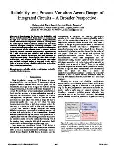
Soft Error Vulnerability Aware Process Variation Mitigation Xin Fu, Tao Li and José A. B. Fortes Department of ECE, University of Florida
[email protected],
[email protected],
[email protected]
Abstract As transistor process technology approaches the nanometer scale, process variation significantly affects the design and optimization of high performance microprocessors. Prior studies have shown that chip operating frequency and leakage power can have large variations due to fluctuations in transistor gate length and sub-threshold voltage. In this work, we study the impact of process variation on microarchitecture soft error robustness, an increasing reliability design challenge in the billion-transistor chip era. We explore two techniques that can effectively mitigate the effect of design parameter variation while significantly enhancing microarchitecture soft error reliability. Our first technique is entry-based. It tolerates the deleterious impact of variable latency techniques on soft error reliability by reducing the quantity and residency cycle of vulnerable bits in the microarchitecture structure at a fine granularity. Our second technique is structure-based. It applies body biasing schemes to dynamically adapt transistor subthreshold voltage (and hence device-level soft error robustness) to the program reliability characteristics at a coarse granularity. We also combine the two techniques which further produces improved results. Compared to existing process variation tolerant schemes, our proposed techniques achieve optimal trade-offs between reliability, performance, and power. To our knowledge, this paper presents the first study on characterizing and optimizing processor microarchitecture resilience to soft errors in light of process variation.
1. Introduction The continued scaling of CMOS process technology to the nanometer scale has resulted in process variations that lead to significant variability in chip performance and power [1, 2, 6, 7, 41]. For example, recent studies estimate that with advanced process technology, chip frequency loss will be as high as 30% [2]. A 20X increase in leakage power has also been reported [1]. Processor architects are now responsible for quantifying and mitigating the deleterious impact of parameter variations in their design. Process variation (PV) is primarily caused by difficulties controlling sub-wavelength lithography and channel doping. Among the design parameters, gate length (L) and threshold voltage (Vth) are two key parameters subject to large variation. Process variation consists of die-to-die (D2D) and within-die (WID) variations. Die-to-die
variation consists of parameter fluctuations across dies and wafers, whereas within-die variation refers to variations of design parameters within a single die. As technology scales, within-die variation, which is the primary focus of this study, has become more significant and is a growing threat to future microprocessor design [1, 2, 3, 6]. In the past, various techniques have been proposed to boost chip performance and/or save leakage power under the influence of process variation at both the circuit and microarchitecture levels. For example, Liang et al. [18] proposed variable latency register files (VL-RF) to improve chip frequency while tolerating long access latency in the register files. Fine-grained body biasing (FGBB) has been applied within a single chip to mitigate the Vth variation. In [19], Teodorescu et al. further proposed a dynamic FGBB (DFGBB) adaptation scheme to achieve an optimal frequency-leakage power operation for each chip. To our knowledge, existing work on analyzing and mitigating the impact of process variation on microprocessor design has been largely focused on performance and power domains. Another emerging challenge arising from processor design using nano-scale transistors is the rapidly increased on-chip soft error rate (SER) due to the smaller feature size, lower supply voltage, and larger integration scale. Soft errors, or single-event upsets (SEUs), are failures caused by high-energy neutron or alpha particle strikes in integrated circuits. These failures are called soft errors because they do not permanently damage the circuit but do destroy data. Since the soft error rate is inherently related to the device parameters (e.g. L and Vth) [16, 17, 39], as technology advances, the impact of process variation should be taken into consideration by architects in reliability evaluation. Furthermore, techniques aimed at mitigating the process variation should also consider their reliability impact. Nevertheless, at the microarchitecture level, there has been no prior work on (1) characterizing the impact of parameter variation on soft error robustness, and (2) optimizing soft error reliability in light of process variation. In this paper, we characterize the impact of process variation on the processor microarchitecture soft error vulnerability. We find that although the critical charge (a widely used metric to evaluate the raw SER) varies significantly under process variation at the bit level, it exhibits small variation at the entry level of microarchitecture structures. We examine the impact of two recently proposed process variation tolerant
techniques (e.g. VL-RF [18] and DFGBB [19]) on microarchitecture soft error reliability and find that both techniques increase the SER. We propose reliability-aware process variation tolerant mechanisms that are capable of achieving an optimal vulnerability-frequency-leakage operating point. To our knowledge, this is the first work to link process variation with microarchitecture soft error reliability and mitigate its impact while considering reliability, performance, and power factors. The contributions of this work are: • We perform a comprehensive study to characterize the impact of process variation (PV) on microarchitecture soft error reliability. We observe that critical charge at the bit level exhibits variation of 18.9%, yet only varies slightly (smaller than 3.5%) at the entry level of microarchitecture structures. We propose a new metric to quantify microarchitecture reliability in the presence of process variation. Our PV-aware architectural vulnerability factor (PV-AVF) extends the cycle-based AVF metric [20] by incorporating the effect of dynamic frequency variation due to PV and PV tolerant mechanisms. We observe that the previously proposed PV mitigation techniques (e.g. VL-RF, DFGBB) degrade microarchitecture soft error robustness. • We propose two techniques, i.e. Entry-Based Vulnerability Mitigation (Entry-BVM) and StructureBased Vulnerability Mitigation (Structure-BVM), that work at fine-grain (entry-based) and coarse-grain (structure-based) levels to perform reliability-aware PV mitigation and achieve optimal vulnerability, performance, and power trade-offs. We perform case studies on the issue queue (IQ) and our proposed techniques are applicable to other structures. Detailed simulation results show that the Entry-BVM improves IQ reliability under PV by 24% with 27% improvement on the trade-offs across all domains. The Structure-BVM reduces IQ vulnerability by 20% with 26% improvement on the trade-offs. The combination of the two proposed techniques reduces IQ SER by 40% and improves the trade-off by 46%. This paper is organized as follows. Section 2 describes our experimental methodology. Section 3 presents our characterization of the impact of PV on microarchitecture soft error susceptibility and analyzes the reliability effect of two recently proposed PV tolerant mechanisms. Section 4 proposes process variation mitigation techniques that are aware of soft error reliability. Section 5 evaluates the proposed techniques in terms of reliability, performance, and power. We discuss related work in Section 6 and conclude our work in Section 7.
2. Experimental Methodology This section presents a model of process variation and describes the methodology we use to estimate the impact
of PV on soft error robustness. In addition, a method to compute the microarchitecture-level soft error reliability is introduced.
2.1. Process Variation Modeling Process variation is a combination of random effects (e.g. random dopant fluctuations) and systematic effects (e.g. lithographic lens aberrations). Random variation refers to random fluctuations in parameters from die to die and device to device. Systematic variation, on the other hand, refers to the layout-dependent variation through which nearby devices share similar parameters. Devices exhibit spatial correlations within a given die. D2D variation mainly exhibits as a random variation, whereas WID variation is composed of both random and systematic variation. We model variations on L and Vth since they are the two major process variation sources [2]. L and Vth in each device can be represented as follows: L=Lnom + ΔLD 2 D + ΔLWID (Eq. 1), Vth =Vth nom + Δ VthD 2 D + Δ VthWID
where Lnom
and
Vth nom
(Eq. 2),
are the nominal value of gate length
and threshold voltage respectively. ΔLD 2 D and ΔVth represent the D2D variations. Devices in a single die share D2D
ΔV
th which are generally constant the same ΔLD 2 D and offsets. ΔLWID and ΔVth represent the WID variation which D2D
WID
can be further expressed as the additive effect of systematic and random variations. We focus our PV modeling on within-die variation since die-to-die variation can be modeled as an offset value to all the devices within the chip. 0,1 0,1 1,4
1,2 1,1
2,2 2,1
1,1
1,2
1,3
1,4
1,3
2,4
2,1 2,2 2,3 2,4 2,5 2,6 2,7 2,8 2,9 2,10 2,11 2,12 2,13 2,14 2,15 2,16
2,3
Figure 1. Multi-level quad-tree partitioning to model systematic variation
To model the random effects of WID variation, we generate random variables that follow a normal distribution. To model systematic variations, we use the multi-level quad-tree partitioning method proposed in [21], which has been widely used in prior work [4, 18, 22]. Figure 1 illustrates this method. A chip is covered by several layers and each layer has a number of quadrants. Each quadrant is assigned a random variable (following a normal distribution) and all devices in the same quadrant share the same value. The systematic variation of each device within the chip is equal to the sum of the random variables of the quadrants, through all the layers, to which it belongs. Nearby devices share more quadrants than far away devices. For example, as shown in Figure 1, devices
in quadrant (2,1) and (2,2) share the random variables in quadrant (0,1) and (1,1), but devices in quadrant (2,1) and (2,16) only share quadrant (0,1). This approach effectively captures the spatial correlation between devices. We chose an area of 32 6T SRAM cells as the granularity of the smallest quadrant, which is sufficient to capture systematic variation. The WID variation follows a normal distribution (random variables are generated through Monte-Carlo simulation) with a standard deviation
σ = σ rand 2 + σ sys 2
,
where σrand and σ sys represent the standard deviation for random and systematic variation respectively. In this study, we simulate processors developed using 45nm process technology and assume σ / μ = 12% and σ rand = σ sys = σ / 2
based on variability projections from [23]. We use the Alpha 21264 as our baseline machine. The layout is scaled down to 45nm from an Alpha 21264 chip floor-plan and 400 chips are generated for statistical analysis. Predictive Technology Models [24], the evolution of previous Berkeley Predictive Technology Models (BPTM), are used to provide the basic device parameters for HSPICE simulations.
2.2. Impact Vulnerability
on
Circuit-Level
Soft
Error
The circuit-level SER can be expressed by the following empirical model [25]: SER ∝ F ⋅ ( Ad , p + Ad , n ) ⋅ K ⋅ e
−
Q crit Qs
WordLine
Vbit_bar M2
Vbit
VDD
will be flipped after Q drops below VDD / 2 , and a soft error occurs. The estimation of critical charge can be expressed as follows: Tf
Q crit =
∫I
d
dt
(Eq. 4), where Tf is the flipping time and Id is the drain current induced by the particle. Device parameters (e.g. L, Vth) impact both Tf and Id, suggesting their effect on Qcrit. We insert a current source (shown in Eq. 5) into node Q to model the particle strike: Q τ ( e − t /τ α − e − t / β ) I in ( t ) = τα −τ β (Eq. 5), where Q is the charge deposited as a result of particle strike, τ α is the collection time constant of the junction, 0
and τ β is the ion-track establishment time constant. Figure 3 depicts the impact of PV on SRAM Qcrit. This figure plots two sets of our experimental results showing how voltages change when a SRAM with process variation (shown in Figure 3(a)) and without process variation (shown in Figure 3(b)) are attacked by the same particle at 100 picoseconds. {V(Q), V(QB)} refers to the voltages of Q and QB without PV and {V(Qpv), V(QBpv)} refers to the voltages of Q and QB with PV. As can be seen, V(Q) and V(QB) maintain the initial state and tolerate the strike while V(Qpv) and V(QBpv) reverse quickly after the strike, leading to a failure. Note that PV also has positive effect on critical charge since parameters can vary up and down around the mean value. Q Voltage at Q keeps as '1'
Particle strike Voltage (V)
(Eq.3), Where F is the total neutron flux within the whole energy spectrum, Ad,p and Ad,n are the p-type and n-type drain diffusion areas which are sensitive to particle strikes, K is a technology-independent fitting parameter, Qcrit is the critical charge, and Qs is the charge collection efficiency of the device. A soft error occurs if the collected charge Q exceeds the critical charge Qcrit of a circuit node. Eq.3 shows that the SER increases exponentially with reduction in Qcrit. In this study, we use the variability of critical charge under process variation to estimate the raw SER variation at the circuit level.
line is not asserted, transistors M5 and M6 disconnect the cell from the bit lines and the two cross-coupled inverters formed by M1~M4 reinforce one another, maintaining a stable state in the cell. There are only two stable states (each state corresponds to store ‘0’ or ‘1’) in the SRAM: Q=0 and QB=1 or Q=1 and QB=0. When energetic particles hit Q (assuming Q=1) and discharge it, M2 begins conducting and charges QB. The state of the cell
M3
Voltage at QB keeps as '0'
Particle strike QB
QB M5
Q M1
M6
Time (s)
M4
(a) without PV Qpv
Insert Current (A)
0.01 0.008 0.006
Voltage at QBpv increases to '1'
Particle strike
0.004 0.002 0.0
0.1
0.2
0.2
0.3
0.3
0.4
T ime ( ns)
Figure 2. Standard 6T SRAM schematics with current source inserted at Q
There are several types of storage cells (e.g. SRAM, Transmission Gate Flip-Flop, and dynamic latch) and the critical charge in each type is different. As an example, we present our analysis on a standard 6T SRAM in this subsection. Figure 2 shows the schematic. When the word
Voltage (V)
0
Voltage at Qpv drops to '0'
Particle strike QBpv
Time (s)
(a) in the presence of PV Figure 3. V(Q) and V(QB) of SRAM (in 45nm process technology) under a particle strike
We model the critical charge variability of different types of storage cells and combinational logic (e.g. chain of 6 inverters, 2-input NAND gate) using the SER- Qcrit model and HSPICE simulations similar to the one described above. The L and Vth of transistors are established using random variables from Monte-Carlo simulation. Figure 4 shows the chip-wide critical charge variation map obtained from our experiments (data are presented in units of fC). The results, which exhibit an average variation of 18.9% across the simulated chips, show that there is large variation in the critical charge under PV. Since SER is exponentially related to critical charge, one can expect an even larger variation in the SER in the presence of PV.
Figure 4. Critical charge variation map for a chip (data are presented in units of fC)
2.3. Microarchitecture-Level Vulnerability Analysis
Soft
Error
A key observation on the effect of soft error at the microarchitecture level is that a SEU may not affect a processor state that is required for correct program execution. The overall microarchitecture structure’s soft error rate without the impact of PV, as given in Eq. 6 [26], is determined by two factors: the FIT rate (Failures in Time, which is the raw SER at the circuit level), mainly determined by circuit design and process technology, and the architecture vulnerability factor (AVF)1. SER = FIT ⋅ AVF (Eq. 6) A hardware structure’s AVF refers to the probability that a transient fault within that hardware structure will result in incorrect program results. Therefore, the AVF, which can be used as a metric to estimate how vulnerable a hardware structure is to soft error during program execution, is determined by the processor state bits required for architecturally correct execution (ACE) [20]. At cycle level, the AVF of a hardware structure is the percentage of bits that are ACE within that structure. At program level, the AVF of a hardware structure is derived by averaging cycle-level AVF of the structure across program execution [20], as shown in Eq.7: AVF =
1
∑
# ACE bits per cycle
execution _ cycles
# B ⋅ Texecution _ cycles
(Eq. 7),
We integrate the timing vulnerability factor (TVF) into the FIT.
where #B is the number of bits in the structure. As can been seen, AVF is primarily determined by the quantity of ACE bits per cycle and their residency time within the structure. Note that Eq. 7 assumes that the frequency is constant. However, the frequency may vary throughout execution due to PV mitigation techniques (e.g. DFGBB boosts chip frequency [19]). To quantify the architecture vulnerability factor in light of process variation, we propose a PV-aware vulnerability metric AVFpv, which is expressed as follows:
∑
AVF pv =
# ACE bits per cycle f pv 1 #B⋅ ∑ execution _ cycles f pv
execution _ cycles
(Eq. 8), where fpv is the frequency under the influence of PV mitigation techniques. Since the FIT/bit (determined by the critical charge) can have large variations due to PV, it is not appropriate to use a random bit’s FIT to compute the entire microarchitecture structure’s FIT (Note that without PV, the FIT of a structure is the product of FIT/bit and the number of bits in the structure) and obtain the SER. An analysis cell should be introduced, which can be as small as a single bit or as large as the entire structure. Each bit within a cell is assumed to share the same FIT/bit and the overall structure’s SER under PV (SERpv) can be expressed as: SER pv =
∑
FITpv _ cell ⋅ AVFpv _ cell
(Eq. 9), where FITpv_cell and AVFpv_cell represent FIT and AVFpv of the finest analysis cell in the structure. Note that even though we assume each bit’s FIT within an analysis cell is identical, we still compute AVFpv at the bit level. # of cells
3. Microarchitecture-Level Soft Error Vulnerability Characterization under Process Variations In this section, we perform an extensive study estimate FIT variation across the analysis cells. addition, the impact of PV mitigation techniques microarchitecture-level soft error vulnerability presented.
to In on is
3.1. FIT Variation across the Analysis Cells In Section 2.2, we introduce a method to quantify critical charge variation at the bit level. At the microarchitecture level, data within a structure are usually accessed on a per-entry basis. Therefore, a characterization of the critical charge variation at the entry level (Qcrit_entry) can provide further insight for exploring reliability-aware PV optimizations. In this section, we present a Qcrit_entry variation analysis for the register file and the same characterization procedure has been applied to other microarchitecture structures. For a given microarchitecture structure, the analysis cell is set to be equal to the size of one entry of that microarchitecture structure. In our study,
Critical Charge (fC)
we opt to use the minimum critical charge as the Qcrit_entry. Since a low critical charge increases the FIT rate, by choosing the minimum critical charge we base our estimation on the bit that is the most critical in determining the upper bound SER of an entry within the microarchitecture structure. We obtain a Qcrit_entry distribution for each chip’s register file and present data from the chip with the largest Qcrit_entry variation. 21 19 17
23 21 19 17 15 13 11 9 7 0
15
16
32
48
VL-RF
80
64
Baseline
70
B it ID (To ta l 6 4 )
13
60
11 9 7 0
10
20
30
40
50
60
70
80
IQ AVF (%)
Critical Charge (fC)
23
but take two cycles in slow entries. These slow entries are not accounted for during register file frequency calibration. n% VL-RF defines the RF frequency based on the slowest read time of the fastest n% RF entries for each read port. The frequency is pre-defined by testing the read ports in each RF entry. In VL-RF, it is possible that a RF entry will have both slow and fast read ports. When a slow port is assigned to a read operation, one cycle stall is encountered in the pipeline that the port belongs to, and consequently, the issue width for the next cycle shrinks and IPC is reduced.
E n tr y ID (T o ta l 8 0 )
50 40 30 20 10
Figure 5. Qcrit_entry of each entry in the register file (80 entries, each entry contains 64 bits)
0
75
150
225 Time (ms)
300
375
Figure 7 (a). IQ AVF in baseline case and VL-RF technique on gcc over a period of 375ms
Critical charge at bit level 16 14
8 6
# of issue pipe stalls
4 2 0 6.5
8
9.5
11
12.5 14
15.5 17 18.5 20 21.5 23
Critical charge (fC)
Figure 6. Entry- and bit- level Qcrit distribution in the register file
Figure 5 shows each entry’s Qcrit_entry within the 80entry register file and a zoom-in view of the entry with the minimum Qcrit_entry by displaying each bit’s critical charge within that entry. Figure 6 plots both the entry-level and bit-level critical charge distribution within the register file. The standard deviation of the entry-level critical charge (3.5%) is much smaller than that at the bit level (25.9%). This is because a large portion of bit-level critical charge variation is smoothed out at the entry level (shown in Figure 5). We can conclude that Qcrit_entry only changes slightly within the structure under PV.
3.2. Microarchitecture Soft Error Vulnerability under Process Variation Mitigation Techniques In this section, we evaluate the impact of PV mitigation techniques on microarchitecture soft error vulnerability. 3.2.1 The Effect of Variable-Latency Register File (VLRF) The multi-ported Register File (RF) is a critical component in determining both the frequency and IPC of a processor. Delay in the register file is dominated by the SRAM access time. Frequency loss within the register file due to process variation can be reduced by applying variable-latency (VL) techniques. In [18], for each read port in the register file, entries are partitioned into fast and slow entries based on the SRAM read delay. Read operations can complete within one cycle in fast entries,
IQ AVF difference between VL-RF and baseline 80
1.6 # of stalls in issue stage
10
60
1.2
40 0.8 20 0.4
IQ AVF (%)
12 Bit count (total 64)
Entry count (total 80)
Critical charge at entry level 45 40 35 30 25 20 15 10 5 0
0
0
0
-20 0
75
150 225 Time (ms)
300
375
Figure 7 (b). The # of issue pipe stalls and IQ AVF difference between VL-RF and baseline case
[18] evaluated the effect of VL-RF on performance. In this paper, we perform a complementary evaluation of its impact on reliability. The issue queue (IQ) is a good starting point for such an investigation since shrinking the issue width directly affects the instruction issue within the IQ. It is important to note that since the bandwidths of other stages (e.g. fetch, renaming, etc) are not affected when a slow read port is selected, only the number of instructions exiting the IQ is reduced and the number of instructions entering the IQ remains the same. As a result, the IQ holds a larger number of instructions and the quantity of ACE bits within the IQ increases correspondingly. Moreover, the slow read operation on RF will cause back-to-back and dependent instructions to wait for an extra cycle, extending their residency cycles within the IQ. Compared to the baseline case that includes PV but not fast/slow RF entries, IQ AVF increases since both the quantity and residency time of ACE bits are increased. Figure 7(a) compares the IQ AVF of the baseline case to that of using the VL-RF technique on the benchmark gcc over a period of 375ms at 1ms granularity. Figure 7(b) plots the IQ AVF differences between the two and the average number of issue pipe stalls during the interval. As can be seen in Figure 7(a), the IQ AVF in VL-RF is substantially higher than that in the baseline case. As the number of issue pipeline stalls climbs to a high level, there
is a corresponding increase in the IQ AVF difference between VL-RF and the baseline case (shown in Figure 7(b)). This illustrates the degradation in soft error robustness that is introduced with VL-RF, and suggests that this degradation is largely a result of the pipeline stalls. In order to mitigate the IPC loss due to VL-RF, [18] proposed a port switching technique that switches from slow ports to fast ports when reading from the RF. This technique compensates for IPC loss by avoiding a large portion of reads from slow ports. This produces fewer pipeline stalls, and the high IQ AVF caused by VL-RF is also mitigated. However, port switching cannot eliminate the use of slow ports and therefore the IQ AVF is still higher than the baseline case. In Section 4.1, we propose a novel variable latency based PV tolerant technique that can significantly improve microarchitecture soft error robustness. 3.2.2 The Effect of Dynamic Fine-Grained Body Biasing (DFGBB) Critical Charge (fc)
25 20 15 10 5 0 -0.18
-0.02
0.14
0.30
ΔVth (v)
Figure 8. Critical charge vs. ΔVth in range of [-0.3v, 0.3v] in 6T SRAM
Body Biasing (BB) applies a voltage between the source or drain and substrate to adjust the threshold voltage. Forward body biasing (FBB) decreases the Vth, decreasing the delay of the transistors - but making them leakier. Contrarily, reverse body biasing (RBB) increases the Vth, creating less leaky but slower transistors. The impact of body biasing on storage cells’ SER has been studied in the past. [38] found that FBB has the ability to improve a flip-flop’s soft error robustness by 35% and RBB degrades the SER by 36% in 130nm process technology. To evaluate the effect of body biasing on an SRAM’s SER in 45nm technology, we compute the critical charge using HSPICE simulations by biasing Vth in the range of [-0.3v, 0.3v] in 6T SRAM with a resolution of 0.032v. Results are presented in Figure 8 ( ΔVth is equal to the subtraction of Vth after BB has been applied from the original Vth. FBB corresponds to positive ΔVth since it reduces Vth and RBB corresponds to negative ΔVth as it increases Vth). As can be seen, there is a linear relationship between critical charge and Vth, and critical charge reduces as Vth increases. Compared to the baseline case without Vth biasing, the critical charge increases 44% with a forward body biasing of 0.3v, and decreases 33% when a reverse body biasing of 0.3v is applied. Since the SER is
exponential to the critical charge, the impact of the varying Vth on the SER will be further amplified. To mitigate the impact of PV on performance under a pre-defined power budget, Static Fine-Grained Body Biasing (SFGBB) is applied during the chip calibration time. It partitions the chip into cells, and statically sets each cell’s body biasing value under the worst case (e.g. the cell is fully loaded in the worst case temperature). Recently, Teodorescu and Torrellas proposed Dynamic Fine-Grain Body Biasing (DFGBB) scheme [19], which allows bias voltages to adapt to dynamic conditions. Take a cell which is initially slow for example, SFGBB applies forward body biasing at the calibration time. With DFGBB, each cell’s body biasing value is set to be the SFGBB value when it is first powered-up. DFGBB dynamically reduces the forward body biasing or even apply reverse body biasing to save the leakage power when the cell is under-loaded. Conversely, when the cell is fully loaded, the temperature increases which results in a frequency loss, DFGBB increases forward body biasing value to improve the frequency. As can be seen, DFGBB is able to reduce the power overhead by adjusting the body biasing value of the cell to the dynamically changing workload. DFGBB, however, ignores the reliability domain characteristics during body biasing adaptations and results in reliability degradation. For example, when an L2 cache miss occurs and the pipeline stalls, cells such as the IQ and ROB buffer large numbers of instructions, leading to a high AVF. In this scenario, DFGBB will reduce the forward body biasing or even apply reverse body biasing, and as a result, degrade the soft error robustness because of the associated decrease in the critical charge. On the other hand, when the structure has a high throughput and the instructions’ residency time is short, the AVF is low. In this situation, DFGBB will increase the forward body biasing that is applied since the temperature is increased. This forward body biasing reduces the FIT (affected by critical charge) but the SER improvement is limited due to the already low AVF. To summarize, DFGBB does not effectively capitalize on opportunities to reduce a structure’s vulnerability. In Section 4.2, we propose a body biasing based PV mitigation technique considering reliability, performance, and power factors.
4. Reliability-Aware Mitigation
Process
Variation
As discussed in Section 3, previous PV mitigation techniques degrade microarchitecture soft error robustness. In this section, we propose reliability-aware PV tolerant schemes that are capable of (1) mitigating microarchitecture soft error vulnerability and (2) achieving an optimal trade-off between performance, reliability and power in the presence of PV.
4.1. Entry-Level Mitigation
Granularity
Vulnerability
We propose a technique that operates at a fine granularity to reduce IQ vulnerability based on VL-RF with port switching (VL-RF+PS). We call our technique Entry Based Vulnerability Mitigation (Entry-BVM). Note that port switching is not an essential requirement for our technique, but our method is adaptable to VL-RF. Our goal is to mitigate IQ AVF without loosing the performance improvement obtained by VL-RF+PS. Since high IQ AVF is a result of both a large quantity of ACE bits and the long residency cycles of ACE bits in the IQ, to reduce IQ AVF both of these factors should be considered. Instructions can be classified as ACE or un-ACE depending on whether their computation results affect the final program output. Most of the bits in an ACE instruction are identified as ACE, while only a small portion of the bits (e.g. the opcode) in an un-ACE instructions are ACE. Assigning ACE-ready instructions a higher issue priority than un-ACE instructions can reduce the residency time of ACE bits because these instructions will be removed from the IQ more quickly, reducing the number of resident ACE bits. Greater reliability benefit is gained when the issue width decreases due to slow RF reads. As the issue pipe becomes more competitive, granting an issue request to an ACE instruction can reduce its probability of waiting extra cycles within the IQ. As described in [20], an instruction cannot be characterized as ACE or un-ACE until its dependence chain has been determined. This can be difficult to accomplish at run time, but there are several methods available to characterize ACE instructions on the fly. A method that uses a SlicK table is proposed in [27] to identify ACE instructions by taking advantage of the time lag between the leading and trailing threads. This method, however, is not adaptable to our design. In [28], a critical table was proposed to quantify an instruction’s criticality. The rationale of this approach is that performance critical instructions usually have a large number of dependent instructions and their computation results are likely to be propagated to the program final output. Consequently, there is a large overlap between ACE and performance critical instructions. In our study, we apply the criticalitybased approach to dynamically identify vulnerable instructions: instructions with high criticality are assumed to be ACE instructions. Note that we still perform rigorous AVF computation [20] in our technique evaluation (Section 5). With VL-RF+PS, a large number of ACE bits in the IQ are created by the imbalanced bandwidth between the issue stage and the other pipeline stages. In [18], a stall signal is generated and sent to the issue stage when a slow RF read occurs. In Entry-BVM, this signal is also sent to other pipeline stages since the input/output imbalance should be avoided in all pipeline stages if possible. For
example, if the dispatch stage were the only stage to receive the stall signal, the decode buffer would have to tolerate the imbalance and the vulnerability would migrate from the IQ to the decode buffer. The only exception is the commit stage since reducing the commit width degrades the IPC. In Entry-BVM, RF entries with a larger number of fast ports are assigned a higher renaming priority, and by doing this, slow RF entries are avoided. This has a positive effect on IPC and helps to compensate for the performance loss caused by issue width reduction. Similar to VL-RF+PS, the per-port speed information for registers is loaded from a ROM which records all of the precollected port speed information for each RF entry. Therefore, it is straightforward to obtain the number of fast ports within the registers. To implement this approach, two bits describing the fast port quantity in the 4-port RF entry are added into the free list macro. These bits are read when selecting free physical registers for register renaming. FETCH
DECODE
RENAME
WAKEUP
SELECT 4
1
Int Register Renaming table
Fast RF rename first
Int Issue Queue
REG READ
EXECUTE
Stall Signal 3
ACE inst issue first
Int Register File
ALU
2 Vulnerability Check Table for Dynamic Vulnerability Identification
Figure 9. Entry-BVM architectural overview
Figure 9 presents an architectural overview of EntryBVM. Floating point structures are omitted due to space limitations, but are similar to the integer structures. Note that Entry-BVM is based upon VL-RF+PS. The detailed implementation of VL-RF+PS, such as the slow and fast RF entry pre-partitioning, VL-RF frequency predefinition, and the circuit support (e.g. latches, MUX) for port switching, is described in [18]. In the renaming stage, registers with a large number of fast ports will be given higher priority when selecting from the free physical register pool. The critical table is added to implement dynamic vulnerability identification. The table is updated when an instruction is renamed in order to record up-todate dependence chain information. For each instruction within the IQ, the table provides the number of dependent instructions in the pipeline. A larger number represents a higher performance criticality. Upon table lookup, instruction criticality is provided to the IQ. This is done in parallel with the instruction wakeup stage and does not introduce any delay into the pipeline. Instructions are recognized as ACE (“1”) or un-ACE (“0”) if their criticality is higher or lower than a given threshold. The request signal accompanied by the vulnerability (“1” or “0”) information is sent to the selection logic when the instruction becomes ready. The selection logic grants the request signal, taking into consideration the vulnerability information. In the register read stage, the stall signal will
4.2. Structure-Level Granularity Vulnerability Mitigation In order to fully exploit soft error robustness improvement opportunities while achieving optimal tradeoffs between vulnerability, performance and power, we propose coarse-grain, Structure Based Vulnerability Mitigation (Structure-BVM) techniques which use two metrics - AVFpv and IPC*fpv - to guide dynamic body biasing adaptations. Although IPC is a widely used performance metric, it is not suitable for measuring performance across chips with variable frequencies. In our scheme, IPC*fpv is used for performance evaluation. Similar to [19], Structure-BVM is implemented based on SFGBB where the body biasing value is statically set for the worst-case execution environment. The maximum forward body biasing applied to Structure-BVM is the body biasing value determined by SFGBB since the power consumption cannot exceed the upper bound power overhead. The AVF of a microarchitecture structure exhibits significant variation at runtime [29, 30] and it is possible to achieve a considerable SER improvement by reducing the raw FIT when AVF is high. Since both AVFpv and IPC*fpv are considered in Structure-BVM and do not always exhibit a strong correlation (i.e. high IPC does not always imply a high AVF, and vice versa), we propose the categorization of program execution into four types of phases based on AVFpv and IPC*fpv; namely high AVFpv + high IPC*fpv, high AVFpv + low IPC*fpv, low AVFpv + high IPC*fpv and low AVFpv + low IPC*fpv. The boundary of a phase is the mean value of AVFpv and IPC*fpv, which equally partitions the two combined parameters into four sets. Consequently, the number of times we apply FBB and RBB will be roughly equal, avoiding the substantial power overhead of over using FBB or the performance loss of over using RBB. The above two-dimensional partition allows us to explore desirable trade-offs across multiple domains (e.g. reliability, performance and power). For instance, a high AVFpv phase will require the application of forward body biasing to gain the highest degree of soft error robustness; and a higher AVFpv corresponds to a higher forward body biasing value. On the other hand, for a low AVFpv phase, we can apply reverse body biasing to save leakage power with negligible effect on SERpv; similarly a lower AVFpv corresponds to a higher reverse body biasing value. However, overall performance may be reduced significantly when reverse body biasing is applied during a phase of low AVFpv + high IPC*fpv. Because of this,
reverse body biasing will not be applied if the total performance cannot be maintained at a level comparable to the baseline case with process variation without any optimization. While in a phase of low AVFpv + low IPC*fpv, the use of reverse body biasing will be less constrained since its negative effect on performance is small. Figure 10 illustrates how forward body biasing and reverse body biasing are applied in each phase in our proposed scheme. IPC*f pv M ean_IPC*f pv
FBB
FBB
RBB
if no perfermance loss then RBB else no BB
Figure 10. BB in each phase 1. 2. 3. 4. 5. 6. 7. 8. 9. 10. 11. 12. 13. 14. 15. 16. 17. 18. 19. 20.
Every 1ms { AVFpv and IPC*fpv computing(); Max, Min and Mean values updating(); Perf_gain computing(); if AVFpv belongs to [Mean_AVFpv, Max_AVFpv] then { AVF_step = (Max_AVFpv – Mean_AVFpv)/FBB_steps; BB = Max_FBB*(AVFpv-Mean_AVFpv)/AVF_step; } else { AVF_step = (Mean_AVFpv – Min_AVFpv)/RBB_steps; BB = Max_RBB*(Mean_AVFpv-AVFpv)/AVF_step; if IPC*fpv > Mean_IPC*fpv and Perf_gain < 0 then BB = 0 } }
Figure 11. Structure-BVM Pseudo-code
We present the pseudo code of our technique in Figure 11. Body biasing is adjusted at an interval granularity with a length of 1ms. At the beginning of each interval, the AVFpv and IPC*fpv of the last interval are computed (the temperature effect on fpv is also considered in our study). Their maximum, mean and minimum values are updated correspondingly. The performance effect due to body biasing is evaluated, which consists of the product of the last interval’s IPC and the frequency difference with and without body biasing applied within the interval. The overall performance impact (perf_gain) is updated correspondingly. The AVFpv and IPC*fpv of the current interval are predicted to be the same as last interval, and the body biasing value for the current interval is determined by AVFpv. The total performance effect and IPC*fpv are used to check whether RBB should be applied. Since the body biasing value is discrete, we partition [mean AVFpv, maximum AVFpv] into smaller, equal ranges. The number of ranges is determined by FBB_steps, which is the total number of FBB steps, and each range corresponds to a FBB value. Similarly, [minimum AVFpv,
mean AVFpv] is partitioned and linked to RBB values. These ranges can be partitioned statically to avoid the overhead of the maximum, mean, and minimum AVFpv updates and dynamic range computations. Since AVFpv can only vary from 0% to 100%, the AVFpv range can be predetermined using information such as the number of body biasing steps that can be applied. Static range partitioning, however, does lose the ability to keep a balanced utilization between FBB and RBB (see Section 5 for a detailed evaluation). As can be seen, Structure-BVM requires online AVF estimation for the structure. The table introduced in Section 4.1 for ACE instruction identification is not applied in Structure-BVM, because every cell that requires AVF computation must access the table. This would introduce a large number of read ports and wires into the table, increasing the power and area overhead. [40] proposed online AVF estimation by performing fault injections during program execution and observing whether the errors result in failures. This requires extra hardware support and results in an area overhead. In this study, we use the methodology proposed in [26], which computes the number of ACE bits by observing the number of instructions read and written into the cell on every cycle, therefore, performs just-in-time vulnerability estimation. The dynamic vulnerability estimation is used to guide body biasing adaptation within the cell and accurate AVF computation is still performed for evaluation purposes. Fine-grain cells within the chip are generally partitioned at the microarchitecture structure level [8] and [19] demonstrates the feasibility of applying body biasing techniques at a per structure level. Note that FGBB is applied independently to each structure, and therefore our technique does not simply migrate vulnerability from one structure to another. To implement body biasing techniques, a bias generator is attached to the structure. It generates bidirectional but equivalent body biasing values for PMOS and NMOS transistors separately, because the same body biasing value has an opposite effect on the two types of transistors. The detailed circuit modifications can be found in [19].
5. Evaluation In this section, we describe our experimental methodology and evaluate the two proposed reliabilityaware PV mitigation techniques. Next, we examine the aggregated effects of the two proposed techniques. Finally, we discuss the area and power overhead.
5.1. Experimental Methodology To evaluate reliability at the microarchitecture level, we use the reliability-aware simulation framework SimSODA [31], which is built on top of a heavily modified and extended Sim-Alpha cycle-level simulator [32]. In addition, we port Wattch [33] into our simulation framework for dynamic power evaluation. The leakage
power is estimated using HotLeakage [34]. The power results are scaled based on technology projections from ITRS [35]. The HotSpot tool [36] is used to estimate chip temperature. We use a default Alpha 21264 machine configuration with 20-entry INT and 15-entry FP IQs, an 80-entry ROB, an 80-entry INT and 72-entry FP register file with 4-rd/2-wr ports, a 32KB L1 D-cache, a 32KB L1 I-cache, and a 2MB L2 cache. The processor pipeline bandwidth is set to four. We use SPEC CPU 2000 integer and floating point benchmarks in our evaluation. The Simpoint tool [37] is used to identify the most representative simulation interval for each benchmark. After that, each benchmark is fast-forwarded to its representative interval before detailed simulation takes place. We simulate 500 million instructions for each benchmark and present the average result across 400 chips. 80% VL-RF is chosen in [18] because it is built on 65nm technology, which has smaller process variation than 45nm technology. For the Entry-BVM technique, we implement 70% VL-RF and obtain a 10% frequency increase compared to the chip without VL-RF. A larger portion of slow RF entries has to be discounted for in order to gain a significant frequency improvement in 45nm. We set the body biasing range as [-0.3v, 0.3v], with a resolution of 32mv. The dynamic FIT computation is based on the linear interpolation shown in Figure 8. Besides mitigating microarchitecture vulnerability in the presence of process variation, our techniques also target achieving the optimal trade-off among reliability, performance and power. We propose a metric Vulnerability-Power/Performance (VPP), which can be SER pv ⋅ power
IPC ⋅ f pv expressed as , to evaluate the cross domain efficiency of the proposed techniques. A better technique will achieve a lower VPP.
5.2. Effectiveness of Entry-BVM We compare our Entry-BVM scheme to VL-RF and VL-RF+PS techniques. Figure 12 a-b shows the IQ SER and performance (IPC*fpv) across the studied benchmarks. Results are normalized to the baseline case without any optimization under the impact of process variation. As expected, VL-RF reduces IQ reliability significantly. For example, the IQ SER increases by 58% on gcc. As can be seen, VL-RF does not introduce a severe IQ reliability degradation on some benchmarks (e.g. equake, mcf). This is because there are a large number of L2 cache misses in those benchmarks which limit the quantity of ready instructions in the IQ for issue. There are still enough pipes for instructions’ issue even though the number of pipes decreases because of VL-RF. Consequently, the IQ AVF is slightly affected by VL-RF. As shown in Figure 12 (a), on average, VL-RF degrades the IQ SER by 18% compared to the baseline case. VL-RF+PS mitigates the negative effect of VL-RF to some degree, but still increases IQ SER by 8%. Entry-BVM exhibits a strong
ability to improve IQ soft error robustness. It not only mitigates the vulnerability increase caused by VL-RF techniques, but further reduces IQ SER by 24%. As Figure 12 (b) shows, the IPC*fpv of VL-RF+PS and Entry-BVM is almost equal, thus Entry-BVM is able to maintain the same performance improvement as VL-RF+PS. Figure 13 shows the trade-off metric VPP across the various techniques. The results are normalized to the baseline case. Entry-BVM produces a much lower VPP than other approaches. On average, the VPP of Entry-BVM is 50% and 28% lower than that of VL-RF and VL-RF+PS respectively. Since Entry-BVM controls the number of input/output instructions to each microarchitecture structure in the entire pipeline via broadcasting the stall signal, it does not migrate the vulnerability from the IQ to other microarchitecture structures. VL-RF
Normalized IQ SER
1.7
VL-RF + PS
Entry-BVM
1.4 1.1 0.8 0.5
gc c cr af ty e pe on rlb m k bz ip ga p vp r tw ol f m c m f gr id sw im fm a3 d m e fa sa ce w re up c w is e ap pl ga u lg am el m eq p ua ke lu ca s A VG
0.2
(a) Normalized IQ SER VL-RF
VL-RF + PS
Entry-BVM
DFGBB
1
Normalized IQ SER
Normalized IPC*fpv
1.1
to adapt to the dynamic AVFpv behavior and choose an optimal BB value. Structure-BVM with dynamic AVFpv range partitioning shows a strong ability to reduce IQ vulnerability. As a result, the IQ SER is 30% and 20% lower than that on DFGBB and the baseline case respectively. The normalized performance (IPC*fpv) results are shown in Figure 15. As can be seen, DFGBB suffers a considerable performance loss even though it maintains the frequency, while Structure-BVM with dynamic AVFpv range partition maintains or improves performance by 22%. This is because the per-interval performance constraint does not incur any negative effect from biasing the threshold voltage. Consequently, performance usually increases. Note that while StructureBVM has an intrinsic power constraint, both DFGBB and Structure-BVM have the ability to reduce the power overhead introduced by SFGBB. One can expect a greater power saving on DFGBB than on Structure-BVM, since Structure-BVM trades off a certain amount of power reduction in improving reliability and performance. Instead of analyzing the power consumption of these techniques, it is more interesting to evaluate the trade-off among the three domains. We present the normalized VPP in Figure 16. On average, the VPP of DFGBB is 40% higher than Structure-BVM with dynamic AVFpv range.
0.9 0.8 0.7
1 0.8 0.6 0.4
VL-RF
VL-RF + PS
Entry-BVM
1.6 1.4 1.2
gc c cr af ty e pe on rlb m k bz ip ga p vp r tw ol f m c m f gr id sw im fm a3 d m e fa sa ce w re up c w is e ap pl ga u lg e am l m eq p ua ke lu ca s A VG
DFGBB
1
static_Structure-BVM
dynamic_Structure-BVM
1.6 1.4 1.2 1 0.8 0.6 0.4 gc c cr af ty e pe on rlb m k bz ip ga p vp r tw ol f m c m f gr id sw im fm a3 d m es fa a ce w re up c w is e ap pl ga u lg e am l m eq p ua ke lu ca s A VG
Normalized VPP
2 1.8
Figure 14. Normalize IQ SER with BB related techniques Normalized IPC*fpv
(b) Normalized IPC*fpv Figure 12. Normalized IQ SER and IPC*fpv yielded by VL related techniques
dynamic_Structure-BVM
1.2
gc c cr af ty e pe on rlb m k bz ip ga p vp r tw ol f m c m f gr id sw im fm a3 d m e fa sa ce w re up c w is e ap pl ga u lg e am l m eq p ua ke lu ca s A VG
0.6
static_Structure-BVM
1.4
0.8
gc
c cr af ty e pe on rlb m k bz ip ga p vp r tw ol f m c m f gr id sw i fm m a3 d m e fa sa ce w re up c w is e ap pl ga u lg am el m eq p ua ke lu ca s A VG
0.6
Figure 15. Normalized IPC*fpv with BB related techniques DFGBB
We first compare our Structure-BVM schemes (using both dynamic and static AVFpv range partitioning) with DFGBB [19] on reliability. Figure 14 presents the IQ SER across the various techniques. Results are normalized to the baseline case. Because DFGBB does not effectively take advantage of FBB to improve soft error robustness, it does not decrease but instead increases the IQ SER by an average of 8% across the studied benchmarks. Compared to the baseline case, the static AVFpv range partition slightly affects IQ vulnerability because it lacks the ability
static_Structure-BVM
dynamic_Structure-BVM
2 1.8 1.6 1.4 1.2 1 0.8 0.6 0.4 gc c cr af ty e pe on rlb m k bz ip ga p vp r tw ol f m c m f gr id sw im fm a3 d m e fa sa ce w re up c w is e ap pl ga u lg e am l m eq p ua ke lu ca s A VG
5.3. Effectiveness of Structure-BVM
Normalized VPP
Figure 13. Normalize VPP on VL related techniques
Figure 16. Normalized VPP with BB related techniques
As shown in Figure 16, the benefit gained from Structure-BVM varies substantially across benchmarks. For example, a large IQ SER reduction is obtained on equake, while the IQ SER on swim is only slightly
changed when Structure-BVM is applied. With StructureBVM, intervals which have close-to-mean AVFpv will be assigned a close-to-zero BB value. If most of an application’s intervals have an AVFpv close to the mean value, the effectiveness of Structure-BVM is reduced. We select one representative chip and show the AVFpv IPC*fpv plot in Figure 17 for intervals on equake and swim respectively. Dotted lines mark the boundaries of the four phases, and an area is drawn with its center (with mean AVFpv and mean IPC*fpv) at the intersection of the boundaries. As is shown, a large number of intervals in swim are covered by the area whereas few intervals in equake are included within the area. 100 90 80 AVFpv (%)
70 60 50 40 30 20 10 0 0
1
2
3
4
5
6
IPC*fpv (10^9)
25
Mean IPC*fpv value AVFpv (%)
20 15 10 5
Mean AVFpv value
0
0
0.5
1
1.5
2
2.5
3
3.5
IPC*fpv (10^9)
Figure 17. AVFpv - IPC*fpv plot for intervals on equake (up) and swim (down) (Intervals within the drawn area are close to the mean value)
1 0.9 0.8 0.7 0.6 0.5 0.4 0.3 0.2 0.1 0 gc
c
cr af ty p e eo n rlb m k bz ip ga p vp r tw ol f m c m f gr id sw im fm a3 d m e fa sa ce w re up c w is e ap pl ga u lg am el m eq p ua ke lu ca s A VG
Normalized IQ SER
5.4. Combining Entry-BVM and Structure-BVM
1 0.9 0.8 0.7 0.6 0.5 0.4 0.3 0.2 0.1 0 gc cr c af ty e pe on rlb m k bz ip ga p vp r tw ol f m c m f gr id sw i fm m a3 d m e fa sa ce w re up c w is e ap pl ga u lg e am l m eq p ua ke lu ca s A VG
Normalized VPP
Figure 18 (a). Normalize IQ SER under Entry-BVM + Structure-BVM
Figure 18 (b). Normalized VPP under Entry-BVM + Structure-BVM
As the results have shown, both Entry-BVM and Structure-BVM exhibit a strong ability to improve a
structure’s soft error robustness. Since they focus on difference levels, they can be combined to further reduce the vulnerability and push the trade-off among the three studied domains closer to an optimal point. Figure 18 (a) and (b) show the normalized IQ SER and VPP under the aggregate effect of Entry-BVM + Structure-BVM across the benchmarks. Compared to the baseline case with process variation, the combined technique reduces IQ SER substantially by 40% while improving VPP by 46%.
5.4. Overhead of Entry-BVM and Structure-BVM It was found in [18] that VL-RF+PS adds a 2% area overhead and less than 5% power overhead. Entry-BVM adds a small amount of logic in register renaming and instruction selection on VL-RF+PS. A n ⋅ n bit table is added for dynamic vulnerability identification, where n is the number of ROB entries. We estimate the extra area overhead introduced by Entry-BVM to be less than 1% and with negligible power overhead. Previous studies have also estimated the overhead of body biasing techniques [8]. Generally, FGBB introduces a 2% area overhead and a 1% power overhead. The timing overhead of FGBB is negligible [19]. Structure-BVM updates several parameters (e.g. AVFpv, IPC*fpv) at the end of each interval, however the processor does not need to stop for these parameter updates. The previous BB can be applied until its re-evaluation is completed, so Structure-BVM introduces no timing overhead. The extra power consumed by the updates is small. There are few circuits and buffers added by Structure-BVM and the estimated extra area overhead is less than 1%.
6. Related Work There have been many studies on characterizing the impact of PV on performance and power. Borkar et al. [1] investigated the impact of PV on both circuit and microarchitecture levels. Bowman et al. [2] introduced maximum clock frequency (FMAX) to model the chip frequency under PV. Orshansky et al. [3] derived a model to estimate the performance degradation for a given circuit and process parameters in the presence of PV. Agarwal et al. [4] presented a statistical timing analysis technique that accounts for WID variations with spatial correlation. Statistical modeling and analysis of leakage power under PV were performed in [5, 6, 7]. There are limited works studying the impact of PV on SER. Ding et al. [10] investigated the impact of L and Vth variations on critical charge separately. Their work was performed at the circuit level and is limited to single storage cells with single parameter variation. Our study extends the SER variation characterization to the microarchitecture level and considers the combinational effect of L and Vth variations. Various PV mitigation techniques have been proposed in the past. Body biasing is widely applied to mitigate both D2D and WID variation [2] or achieve an optimal tradeoff between frequency and power [8]. [9] developed power
optimization techniques considering the PV effect based on the statistical analysis. [15] showed that PV can slow down the issue queue read/write operations and hurt the performance, it proposed instruction steering, operandand port-switching to improve the performance. Tiwari et al. [11] proposed Recycle, which applies cycle time stealing to microarchitecture pipeline stages for frequency improvement. Liang et al. [12] proposed a memory architecture based on novel 3T1D DRAM to tolerate PV. [13] applied two fine-grained tuning techniques- voltage interpolation and variable latency to reduce the frequency variation between chips, between cores on one chip and between units within one core. [14] used linear programming to find the best voltage and frequency levels for each core of the CMP in the presence of PV. However, these PV optimization schemes largely ignore microarchitecture soft error reliability. In this paper, we proposed novel techniques to mitigate the negative PV effect considering reliability, performance and power factors.
7. Conclusions Process variation and soft error rate are two major challenges that need to be addressed as process technology continues to scale down. Most PV related studies focus only on performance and power domains, and little work has been done to link PV to soft error vulnerability. However, an efficient PV mitigation technique should have the ability to take reliability, performance, and power into account. This paper presents the first study to optimize the reliability of PV mitigation techniques while considering all three domains. We characterize the critical charge variation at the bit and entry level in the presence of PV. We propose Entry-BVM and Structure-BVM to improve microarchitecture soft error reliability and its trade-offs with performance and power in light of PV. Simulation results show that Entry-BVM and StructureBVM can reduce IQ SER by 24% and 20% and achieve a trade-offs improvement of 27% and 26% respectively. The combined effect of the two techniques can achieve even higher IQ SER reduction (i.e. 40%) with 46% trade-offs improvement.
Acknowledgements This work is supported in part by NSF grants CNS0834288, CCF-0811611, CNS-0720476, by SRC grants 2008-HJ-1798, 2007-RJ-1651G, by Microsoft Research Trustworthy Computing, Safe and Scalable Multi-core Computing Awards and by three IBM Faculty Awards. José Fortes is also funded by the BellSouth Foundation.
References [1] S. Borkar, T. Karnik, S. Narendra, J. Tschanz, A. Keshavarzi, and V. De. Parameter variations and impact on circuits and microarchitecture. In Proceedings of DAC, 2003. [2] K. Bowman, S. Duvall, and J. Meindl. Impact of die-to-die and within-die parameter fluctuations on the maximum clock frequency distribution for gigascale integration, Journal of Solid-State Circuits, 2002.
[3] M. Orshansky, L. Milor, P. Chen, K. Keutzer, and C. Hu. Impact of spatial intrachip gate length variability on the performance of high-speed digital circuits. IEEE Transactions on Computer-Aided Designof Integrated Circuits and Systems, May 2002. [4] A. Agarwal, D. Blaauw, and V. Zolotov. Statistical timing analysis for intra-die process variations with spatial correlations. In Proceedings of ICCAD, 2003. [5] A. Srivastava, R. Bai, D. Blaauw, and D. Sylvester, Modeling and analysis of leakage power considering within-die process variations, In Proceedings of ISLPED, 2002. [6] H. Chang and S. S. Sapatnekar, Full-chip analysis of leakage power under process variations, including spatial correlations, In Proceedings of DAC, 2005. [7] R. Rao, A. Srivastava, D. Blaauw, and D. Sylvester, Statistical estimation of leakage current considering inter and intra-die process variations, In Proceedings of ISLPED, 2003. [8] J. Tschanz, J. Kao, and S. Narendra. Adaptive body bias for reducing impacts of dieto-die and within-die parameter variations on microprocessor frequency and leakage. In Journal of Solid-State Circuits, 2002. [9] A. Srivastava, D. Sylvester, and D. Blaauw, Statistical optimization of leakage power considering process variations using dual-Vth and sizing, In Proceedings of DAC, 2004. [10] Qian Ding, R. Luo, H. Wang, H. Yang and Yuan Xie, Modeling the impact of process variation on critical charge distribution, In Proceedings of SOCC, 2006. [11] A. Tiwari, S. R. Sarangi, and J. Torrellas. ReCycle: Pipeline Adaptation to Tolerate Process Variation, In Proceedings of ISCA, 2007. [12] X. Liang, R. Canal, G.Y. Wei, and D. Brooks. Process Variation Tolerant 3T1DBased Cache Architectures, In Proceedings of MICRO 2007. [13] X. Liang, G.Y. Wei, and D. Brooks, ReVIVaL: A Variation-Tolerant Architecture Using Voltage Interpolation and Variable Latency, In Proceedings of ISCA, 2008. [14] R. Teodorescu and J. Torrellas, Variation-Aware Application Scheduling and Power Management for Chip Multiprocessors, In Proceedings of ISCA, 2008. [15] N. Soundararajan, A. Yanamandra, C. Nicopoulos and N. Vijaykrishnan, Analysis and Solutions to Issue Queue Process Variation, In the Proceedings of DSN, 2008. [16] V. Degalahal, R. Ramanarayanan, N. Vijaykrishnan, Y. Xie and M, J, Irwin. The effect of threshold voltages on the soft error rate, In Proceedings of ISQED, 2004 [17] R. R. Rao, D. Blaauw, and D. Sylvester. Soft error reduction in combinational logic using gate resizing and flipflop selection, In Proceedings of ICCAD, 2006. [18] X. Liang and D. Brooks. Mitigating the impact of process variations on processor register files and execution units, In Proceedings of MICRO, 2006. [19] R. Teodorescu, J. Nakano, A. Tiwari, and J. Torrellas. Mitigating parameter variation with dynamic fine-grain body biasing, In Proceedings of MICRO, 2007. [20] S. S. Mukherjee, C. Weaver, J. Emer, S. K. Reinhardt, and T. Austin. A systematic methodology to compute the architectural vulnerability factors for a high-performance microprocessor, In Proceedings of MICRO, 2003. [21] A. Agarwal, D. Blaauw, S. Sundareswaran, V. Zolotov, M. Zhou, K. Gala, and R. Panda. Path-based statistical timing analysis considering inter and intra-die correlations, In Proceedings of TAU, 2002. [22] K. Meng, and R. Joseph. Process variation aware cache leakage management, In proceedings of ISLPED, 2006. [23] A. Kahng. How much variability can designers tolerate? Design & Test of Computers, 2003. [24] NIMO Group, Arizona State Univeristy. PTM homepage. http://www.eas.asu.edu/~ptm/. [25] P. Hamcha and C. Svensson, Impact of CMOS technology scaling on the atmospheric neutron soft error rate, IEEE Transactions on Nuclear Science, 2000. [26] N. Soundararajan, A. Parashar, A. Sivasubramaniam, Mechanisms for Bounding Vulnerabilities of Processor Structures, In Proceedings of ISCA, 2007. [27] A. Parashar, A. Sivasubramaniam, S. Curumurthi, SlicK: slice-based locality exploitation for efficient redundant multithreading, In Proceedings of ASPLOS, 2006. [28] S..T. Srinivasan, R.D. Ju, A.R. Lebeck, C. Wilkerson, Locality vs. Criticality, In Proceedings of ISCA, 2001. [29] X. Fu, J. Poe, T. Li, J. Fortes, Characterizing Microarchitecture Soft Error Vulnerability Phase Behavior, In Proceedings of MASCOTS, 2006. [30] K. R. Walcott, G. Humphreys, S. Gurumurthi, Dynamic Prediction of Architectural Vulnerability from Microarchitectural State, In Proceedings of ISCA, 2007. [31] Sim-SODA simulator, http://www.ideal.ece.ufl.edu/sim-soda [32] R. Desikan, D. Burger, S. W. Keckler, and T. Austin, Sim-alpha: A Validated, Execution-Driven Alpha 21264 Simulator, Technical Report, TR-01-23, Dept. of Computer Sciences, University of Texas at Austin, 2001. [33] D. Brooks, et al., Wattch: A framework for Architectural-Level Power Analysis and Optimizations, In Proceedings of ISCA, 2000. [34] Y. Zhang, D. Parikh, K. Sankaranarayanan, K. Skadron, and M. Stan. HotLeakage: A temperature-aware model of subthreshold and gate leakage for architects. Technical Report CS-2003-05, University of Virginia, 2003. [35] International Technology Roadmap for Semiconductors (2006 Update). [36] K. Skadron, M. R. Stan, W. Huang, S. Velusamy, K. Sankaranarayanan, and D. Tarjan. Temperature-aware microarchitecture. In Proceedings of ISCA, June 2003. [37] T. Sherwood, E. Perelman, G. Hamerly and B. Calder, Automatically Characterizing Large Scale Program Behavior, In Proceedings of ASPLOS, 2002. [38] T. Karnik, et al. Impact of body bias on alpha- and neutron-induced soft error rates of flip-flops, Symposium on VLSI Circuits Digest of Technical Papers, 2004 [39] C. Weaver, J. Emer, S. S. Mukherjee and S. K. Reinhardt, Techniques to reduce the soft error rate of a high performance microprocessor, In Proceedings of ISCA, 2004. [40] X. Li, S.V. Adve, P. Bose and J. A. Rivers, Online Estimation of Architectural Vulnerability Factor for Soft Errors, In the Proceedings of ISCA, 2008. [41] O. S. Unsal, J. Tschanz, K. A. Bowman, V. De, X. Vera, A. Gonzalez and O. Ergin, Impact of Parameter Variations on Circuits and Microarchitecture, IEEE Micro, 2006.