Software Radios will have an important role in future terminal and base station ... radio implementations, like power management, quality of service. (QoS), system .... platform is that it incorporates internal bus-like interfaces to FPGAs to.
Software Radio implementation of a DS-CDMA indoor subsystem based on FPGA devices X. Revés; A. Gelonch; F. Casadevall Universitat Politècnica de Catalunya, Dept. of Signal Theory and Communications Jordi Girona 1-3, 08034 Barcelona (Spain) {xreves, antoni, ferran}@xaloc.upc.es
ABSTRACT Software Radios will have an important role in future terminal and base station definition. Although the ideal software radio architecture is highly restricted by technology, at present it is possible to build complex systems completely customised and reconfigurable using the FPGA devices. They provide to the designer the possibility to modify the hardware functional qualities without giving up high performance or poorly use resources. To check how much important is this affirmation considering future wideband systems, a representative DSCDMA subsystem has been built over an FPGA platform that allows fast reconfiguration of internal system blocks.
the fact that the exchange of information between different blocks is simpler than interfacing different chips. Then FPGAs, understood as general devices where any digital process can be implemented, will assume one of the most important role into reconfigurable equipment in terminals and Base Stations. Because of this, FPGA-only-based platforms are used now to prototype radio systems with requirements similar to those of future 3G/4G standards just to analyse which are the best architectures to be used not only to improve area, speed and power consumption as typical parameters to be optimised in a digital system, but also, considering a widespread understanding of the Software Radio concept, where the system architecture must carry out tuning tasks from internal measures and partial or total updates taking into account the QoS that must be achieved in the transmission process.
I. INTRODUCTION The initial period of 3G deployment will require multimode terminals and base stations to provide a clean transition from 2G (or 2.5G) . This period of time will place constraints to the way that radio terminals are built. The Software Radio approach [1] can be an interesting solution to the problems that this evolution imposes. But software radios are not only interesting when dealing with multiband multimode terminals. Many issues can be envisaged to be adequate for software radio implementations, like power management, quality of service (QoS), system upgrade, etc. Widening the range of application of software defined radios adds complexity to the terminal itself but opens an important area where future generations can take advantage. The important theoretical features of software radio terminals clash with the available technology that has, at present, important limitations in terms of bandwidth and dynamic range, clock managing (for multi standard terminals) and high power requirements for high performance digital processing stages. Then, how available and affordable are the different technologies is a key point. In general implementations based on limited-function ASICs (Application-Specific Integrated Circuit) are cheaper than those based on digital signal processors (DSPs) or field programmable gate arrays (FPGA). But ASICs or parameterised hardware have their main drawback in the low level of flexibility that they offer. Instead, DSPs and FPGAs offer flexible methods of modifying their functions. It is generally accepted that DSPs and FPGAs are adequate for different tasks within the transmit/receive chains, being assigned to FPGAs relatively high sample rate filters, correlators, convolvers, FFTs, etc. and being assigned to DSPs algorithms with sequential nature at lower sample rates. Even though FPGAs have still lack of some tools compared to DSPs, what complicates system design, they represent an evolution because of the low power, size and price and the high adaptability to the target design [2]. The previously stated FPGA’s features can be easily extended incorporating, if required, an standard or tuned CPU core allowing an easier reprograming of its tasks. All those functional characteristics, implemented internally in an FPGA based system, are optimised by 0-7803-7244-1/01/$10.00 ©2001 IEEE
In this paper we will deal about implementation of digital stages of an indoor DS-CDMA system focusing on particular architectures well suited for FPGA devices, providing significant figures about resource utilisation. The main goal resides in identifying adequate solutions for each constituent part of the system, on the basis of the predefined architecture of an FPGA, in order to minimise the resource allocation.
II. GENERAL DESCRIPTION A. System Architecture The DS-CDMA [3] indoor system presented here, which works at the 2.4GHz frequency band, has an star architecture where all the terminals interact with its own base station that has the transmission, reception and control capabilities, as user control, channel assignment, code distribution, power control, etc. Each base station can bear up to 64 different channels of 32kbits/s simultaneously assigned to a maximum of 16 different users depending on the QoS required. About the user terminals, there were considered three different kinds of traffic. The first one should be able to manage voice information, using DPCM (Differential Pulse Code Modulation) at 32kbits/sec with 30 msec of maximum delay. For the second one a data flow at 9.6 kbits/sec and delay below 30 msec was assumed. The third traffic types should be able to manage traffic generated by video source using standard H261, with data rates up to 2Mbits/sec. In these cases the bit rate can be adapted from 32kbits/sec to 256kbits/sec in 32kbits/sec steps and delays not exceeding the 100 msec. The CDMA radio link will use traffic channels (TCH) to carry data, voice and video. These channels will be complemented with associated control channels (ACCH) for power control, channel information, status of communication, etc. Other signalling channels used are the pilot channel (PICH), to allow correct synchronism of the mobile to the network, the broadcast paging channel (BPCH), for paging, access to the network or handover, and the random access channel (RACH), to allow the mobile asking a traffic channel.
The parts of this system implemented up to present using an FPGA approach range from the physical channels to intermediate frequency. Due to the fact that the processing gain is high enough, (Spreading Factor of 128), no coding or interleaving has been considered. The
service that the FPGA-based layer provides is a simple raw service of transport of data over the radio channel.
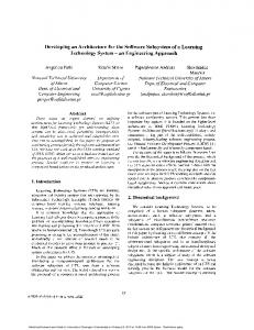
FPGA TX: Base Station (16 users) PICH BPCH
Pre RAKE
?
+ wj
HB FIR
I/Q
I/Q
FIR RRC
HB FIR
N users
MF FIR
4 CHIP SYNC. FRAME SYNC.
MF FIR
4
CHANNEL UNMAP
?
+
FPGA RX: Mobile
FIR RRC
CDMA DEMOD.
Channel Mapping
wi
FED
NCO
CHANNEL ESTIMATOR
Walsh & PN
Figure 1: Down Link Transmitter and Receiver
Shaping Filter (FIR)
Matched Filter (FIR)
I/Q + NCO
I/Q
Shaping Filter (FIR)
Shaping Filter (FIR)
Synchronism Acquisition & Tracking
CDMA Demodulator Diversity Select
Another Receiver
Channel Dec./Control
GOLD
FPGA RX: Base Station (1 user)
DeMUX
MUX
Channel Enc./Control
FPGA TX: Mobile
Figure 2: UpLink Transmitter and Receiver
B. Down Link Structure
C. Up Link Structure
Down Link (see Figure 1) is mainly based on an orthogonal multiplexing of information and control channels using pseudonoise sequences. The sequences used to multiplex channels are called Walsh or Hadamard sequences and those used to isolate adjacent cells are called GOLD sequences. Each user has a maximum of 4 QPSKCDMA channels each of them at 64kbits/s separated by different Walsh sequences at 1024Mchips/s. This provides a maximum of 256kbis/s per user which is the limit assumed in the system.
In this case a simple QPSK scheme was used for transmission where the maximum speed for both, the inphase and quadrature channels, was established in 128 kb/s. This data rate was spread using GOLD sequences up to 4096 kchips/s, obtaining a processing gain of 32 when transmitting at the maximum speed (256 kb/s total). To simplify the design an asynchronous access was implemented, then a synchronism stage in the base station receiver must be implemented. In the Figure 2 the FPGA sections of the Up Link transmitter and receiver schemes can be observed.
In transmission two separated antennas are used to transmit twice the same signal with a determined delay between them longer than the CDMA chip resolution. In the receiver side a RAKE structure can take advantage of this transmission diversity. To simplify the receiver, a pre-RAKE [4] structure is included in the transmitter (base station) for each user which is adjusted using the channel estimation values obtained by the mobile terminal.
III. IMPLEMENTATION A. Block Optimisation Figure 1 and Figure 2 give a general view of the blocks implemented using the FPGA approach for up and down links of the base station and mobile terminal respectively. In each transmitter the information bits are given to the FPGA which generates a QPSK modulation
centred at 8192kHz and sampled at 32768kHz. Inversely, in the receiver the bits are obtained after synchronisation, frequency adjust, channel estimation, etc.
10 bits, 4096 ksps Z-1
Z-1
Z-1
Z-1
Z-1
MUX
Ctrl. Coefficient RAM 16 x 10 bits
Ctrl. Coefficient RAM 16 x 10 bits
10 x 10 P. Multip.
?
S1
S0 0 S1 0
Z-1
MUX
Acc. Out (16384 kHz)
S0
Z-1
Other examples in the transmission/reception chains can be found. After general simplifications, efficiently mapping the block onto FPGA consists mainly on identifying how the algorithm can be translated to the internal structures. The use of internal RAM/ROM and fast adders provides a good mechanism to implement typical signal processing tasks but some times require an algorithm reshaping or even a special control.
+
SN
On the basis of the previously stated simplifications, the FPGA implementation can have different shapes, where considerations about number of bits, number of coefficients, etc. are very important. The first filtering process mentioned can efficiently be implemented as shown in the Figure 3 where only two multipliers with their inputs multiplexed are used to compute the output. In the case of the second filtering process, the transposed FIR structure shown in the Figure 4 fits well to our purposes (and in general in most FPGA FIR implementations). Here the multipliers are implemented as distributed arithmetic multipliers taking advantage that the coefficients of the filter are constants. In both filtering cases FPGA internal RAM and fast internal adders are the key that allow an efficient implementation of the blocks.
SN 0
After cos/sin product (32762 kHz) Figure 3: FIR filter with multiplexed multipliers
B. Reconfigurable Platform As can be observed some blocks in the down link will be similar to those in the up link. But when each block is optimised to reduce the resources required to implement it, reusing the block is not possible. Nevertheless, what is important is to identify which structure better fits to that type of block. What can certainly be reused is the way a function is implemented in every case. Then the concrete implementation can be adjusted in an automatic way. Consider, for instance, two different filtering stages of the down link. First, in transmission, the FIR filter is used to generate a pulse with root raised cosine shape. To this filter only one of every eight input samples is non-zero (4096kHz input zero padded and filtered to get 32768kHz output). The property can be used to reduce the number of multipliers and consequently reduce the amount of logic. Another filtering stage would be the half band filter used in the down link receiver before decimating by 2 (HB FIR). The samples entered to this filter are nonzero and then simplifications can only be done considering the decimation process and through the selection of an adequate filter with, for instance, zero-valued coefficients in every odd sample. Of course until here the simplifications are not only useful for FPGAbased implementations but also for any other kind of implementation.
In
C0
C1
CN-1
Out
X[8:6] X[5:3] X[2:0]
Ci=2123 3b
ROM 8 x 14
14b
+
X[9]
MUX 4-1x3
2-3 22b
+/-
Control Figure 4: Transposed FIR form and multiplier example
The hardware platform used to check the validity of the system is not tuned for this specific design. It is a pre-designed platform with enough flexibility to accommodate different applications. This platform is called SHaRe (Reconfigurable Hardware System) [6] which provides up to 8 user programmable FPGAs interconnected in a flexible way with access to additional resources like RAM, ROM, FIFOs and programmable clocks. Each one of the FPGAs can be (re)programmed individually at any time by simply performing write cycles to a memory address over the host bus (VME bus). This allows distributing blocks along different FPGAs to perform partial and discrete (re)configurations of the system, similarly as it would be with a partially configurable FPGA. One of the design features of the platform is that it incorporates internal bus-like interfaces to FPGAs to accommodate typical CPU accesses moreover of the general purpose interfaces to easily join different blocks. This structure fits with the previously stated idea of inserting CPU cores into FPGAs and linking them to the rest of blocks in a “seamless” manner. The main processor over the VME bus, controlling the whole system, is an Sparc CPU running Solaris. This host processor provides connection to an IP network thus obtaining a higher functionality of the system. The control of the application running over several SHaRe boards is made by means of an information gathering system that captures data from internal blocks and sends them to the host processor which analyse this information to obtain relevant figures about the system behaviour (see Figure 5). For this purpose, the platform bridges the high bandwidth internal simple synchronous bus, that interconnects all the FPGAs, to the external asynchronous VME standard interface. This mechanism allows to redefine the system taking into account the measurements done in real time. In such a case one or more of the FPGAs can be reprogrammed with another configuration to overcome the detected problems or to improve the system performance. Of course the introduction of mechanisms to obtain information from the system internals increments the amount of resources used but this increment can be maintained easily to values around 5-10 % of the system needs. After processing the information obtained and deciding the modifications to be done, two different approaches can be followed to adjust and update the system. One would be through the presence of parameters inside the hardware design that implies the use of registers or look up tables. The other would be modifying directly part of the
VME Bridge
FPGA
Sparc CPU Host VME bus
FPGA IBUS
Interconnect
system taking advantage of the inherent FPGA reconfigurability. Doing system blocs configurable through parameters is not, in general, an optimum solution because it adds overhead in resource allocation and does not offer any advantage in respect of ASIC design option, except the easy update of the whole system block. By other hand, modifying part of the system assumes a new hardware design and synthesis followed by a compilation process that may require a relative long time (compared with hundreds of milliseconds) depending on the design constraints. Until present, this process is complex enough, specially the design stage, to require human skills to be carried out and because of that the process cannot become a completely automatic procedure.
Net
FPGA
SHaRe Figure 5 Simplified platform organisation
board. Also the base station for one user receiver and 16 transmitters fit over a single board, but every new base station receiver requires a new board. With this distribution chosen the maximum number of resources required over a single board is about 9000 LEs that can be obtained completing a SHaRe board with the smallest devices it can bear to achieve the total of 9216 LEs. Although the numbers fit, it is not possible to adjust the design to that level and some room must be considered to install accessories, controls and even leave some resources free to easy the process of mapping of the blocks over the devices. All the boards involved in the design together with the main system controller, a Sparc diskless board for VME bus, are joined over a VME bus to allow a correct configuration and management of the application. In general the blocks have been implemented exchanging area for speed. Reducing area at the cost of an increment of frequency clock does not save power consumption. Power consumption is minimised only when the mapping of a function over FPGA resources is optimally done. Power demanded by the FPGA devices depend highly on the physical properties of them but more advanced the technology used less the power required is. Of course, the flexibility provided by FPGAs over ASICs is paid as an increase of power consumption when the FPGA option is selected. By other hand, the amount of LEs stated here is relatively low compared to the availability of them in commercial FPGAs, so a different structure with higher sampling rates can be considered simply increasing area. Note that in the digital implementation of a radio receiver only the very first filtering stages after sampling have high rates. As soon as the channel of interest has been selected the sampling rate is reduced and/or transformed to be adequate for the required demodulation.
C. Resource utilisation The system roughly described above, although represents a simplification with respect to commercial products, is an example that incorporates all the functions that imply a higher signal processing demand. That is, intermediate frequency processing (this is mainly filtering) and synchronisation algorithms [4]. The blocks that perform these tasks must use resources optimally to both reduce the amount of resources required and also to reduce the power consumption of the devices. This has been one of the main goals of the design. The information here provided of resource allocation is expressed in terms of Logic Elements (LE). One LE is defined as the composition of one 4-input look up table (LUT), equivalent to a RAM of one bit wide an 16 addresses of depth, and one flip-flop. It should be noted that figures given are approximated because are extracted from CAD tools reports where several blocks are mixed and/or other support functions are considered. In Table 1 and Table 2 the LE utilisation for the mobile terminal and base station is summarised. The values concern only to the specific part named. The figures show that the complete terminal system would fit into an state-of-the-art FPGA with about 7000 LEs. This was a huge FPGA some years ago, but today this amount of LEs can be found into relatively small FPGAs like a Xilinx Virtex XCV400 [7]. The base station part for a single user would need less than 9000 LEs which are also available into that FPGA. The increase of resource utilisation for more users (16 in this case) is not linear because most of the transmitter is reused, as it can be observed in the Figure 1 where IF stages are not repeated for each user. In any case, about 100000 LEs should be employed to construct this part of the base station. As stated before, the platform used, called SHaRe, has 8 userprogrammable FPGAs with a count of up to 50176 LEs, 2 Mbytes of SRAM distributed along the devices, up to 512 Kbytes of FIFOs and up to 512 Kbytes of ROM. The mobile terminal fits over a single
Table 1. LEs required to implement the terminal Mobile Terminal Block Description Terminal TX spreading and root raised cosine filters Terminal TX frequency adjust NCO and IF translation Terminal RX I/Q down conversion with half band filter Terminal RX frequency adjust (NCO + FED) Terminal RX matched filters Terminal RX chip, bit and frame synchronism Terminal RX channel estimation and CDMA demodulation Total Mobile Terminal
LEs 400 620 1060 830 1450 1520 500 6380
Table 2. LEs required to implement the basestation Base Station Block Description LEs Base station TX 16 users spreading, pre-RAKE 1140 and PICH + BPCH Base station TX 16 users I/Q shaping filter and 1090 IF translation Base station RX 1 user I/Q down conversion 4390* and matched filters Base station RX 1* user chip synchronism and 1180* tracking Base station RX 1* user CDMA demodulation 500* Total Base Station 16 users 99350 * Multiply by 16 to compute the total base station LE requirements
IV. CONCLUSIONS There are several ways to implement a re-configurable radio terminal but one that offers a wide application flexibility, ranging from high computational intensive tasks to algorithmically complex but relatively low speed tasks, and at the same time flexibility to modify its behaviour, is the one based on FPGAs. Their increasing capacity and speed, together with the progressive reduction of power consumption make of them a good candidate to occupy relevant positions in future radio terminals designed under the Software Radio design methodology. A DS-CDMA system taking advantage of the structural properties of FPGAs has been designed to check their adaptation to that kind of application and to explore the pros and cons when designing specific parts. Like in many digital systems here appears a trade-off between speed and logic resources used: higher is the speed required, higher are the resources required to implement the functions. It has been observed that commercial FPGAs offer the range of resources needed to build a system whit these features. Designing with the FPGA internal pre-defined structures tends to modify the way the different blocks are implemented to efficiently use resources. This, in general, makes impact on the complexity of solution because typical signal processing structures cannot be directly translated. Finding the right mechanism will improve final design in terms of die and power consumption. All that has an interesting application when considering restrictions related to fully digital radio terminals because a better adaptation to FPGA structure will allow to implement more computationally intensive tasks. Because of this, it is important to identify clearly the blocks which require a more accurate tuning and get a set of possible solutions that may fit in many different applications. Also it is important to investigate which are the more interesting architectures for FPGA arrays plus complements (Memory, I/O, programmable clocks, etc.) to extend its flexibility and reusability. To take advantage of the inherent reconfigurability of FPGAs and to analyse the actual system behaviour and apply changes over its configuration a simple method to retrieve information from the application has been built. Nevertheless, it has been found that modifying the FPGA-based radio terminal (or some of its components) is not a simple task. Then has been stated that the data capture, system block analysis and redesign, compilation and deployment processes must become fully automatic in order to achieve the whole Software Radio concept. New and powerful tools for the system block analysis and redesign of FPGA based platforms are required to complete the previous chain and take advantage of the reconfigurability that such devices offer.
REFERENCES [1] C. Taylor, “Using Software Radio in 3rd Generation Communications System”, ACTS Mobile Communications Summit, Aalborg, Denmark, Oct. 1997. [2] M. Cummings, S. Haruyama. "FPGA in the Software Radio". IEEE Communications Magazine. February 1999. [3] F. Adachi, M. Sawahashi, H. Suda, “Wideband DS-CDMA for Next-Generation Mobile Communications Systems”, IEEE Communications Magazine, September 1998.
[4] K. Chapman, P. Hardy, A. Miller, M. George, “CDMA Matched Filter Implementation in Virtex Devices”, Xilinx XAPP212(v1.0), March 2000. [5] R. Esmailzadeh, M. Nakagawa, “Pre-RAKE Diversity Combination for Direct Sequence Spread Spectrum Mobile Communications Systems”, IEICE Transactions on Communications, vol. E76-B, no. 8, pp. 1008-1015, August 1993.
[6] X. Revés, A. Gelonch, F. Casadevall, “Reconfigurable Hardware Platform for Software Radio Applications (SHaRe) in Mobile Communications Environments.” Proc. ACTS Mobile Communication Summit, Sorrento, Italy, June 1999. [7] XILINX Virtex™ 2.5 V Field Programmable Gate Arrays. 2000.
Acknowledgement: This work has been supported by CYCIT (Spanish National Science Council) under grant TIC98-0684.