ISSN 1392 – 1215
ELECTRONICS AND ELECTRICAL ENGINEERING ELEKTRONIKA IR ELEKTROTECHNIKA
2010. No. 4(100)
SYSTEM ENGINEERING, COMPUTER TECHNOLOGY
T 120
SISTEMŲ INŽINERIJA, KOMPIUTERINĖS TECHNOLOGIJOS
Orders Priorities Settings Criteria for Multifunctional Registers Al.Valachi, M. Timis, B. Aignatoaie 1
Technical University “Gh.Asachi” Iasi, Automatic Control and Computer Science Faculty, Computer Science & Engineering Department, e-mails:
[email protected],
[email protected],
[email protected]
S. Tarcau
Special Department of Telecommunications – Bucharest - CK – clock input, active on positive edge signal
Introduction
The thruth table of MFR is illustrated in Table 1:
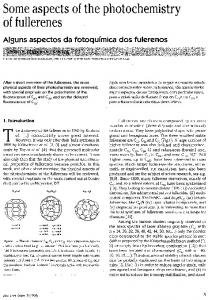
Already are known methods for synthesis of FSM [1], complex digital automata with wired sequencers systems [2], [3], [4], using the multifunctional registers (MFR). In this paper, the authors propose an original method for designing and implementing a MFR register. Let’s consider a such digital register structure like in Fig. 1:
Hold Reset Parall –el Load Shift Right Shift Left Count Down Count Up
SR
d[ p −1: 0]
U/D
Mode
DL
p
L/ R
Table 1. The MFR thruth table
MFR
PE
SH CE CK
DR Q[ p −1: 0]
SR PE SH CE L / R U / D CK
Q[ p − 1 : 0]n +1
x
Q[ p − 1 : 0]n 00…0
x
↑
d [ p − 1 : 0]n
0
x
↑
DRQ p−1 ...Q2 Q1
x
1
x
↑
Q p − 2Q p −3...Q0 DL
0
1
x
0
↑
[Qn − 1] mod 2 p
0
1
x
1
↑
[Qn + 1] mod 2 p
1 1 0 x
0 x
0 x
x x
1
0
x
x
x
1
1
1
x
1
1
1
1
1
1
1
x x
x
Taking account the signals inputs priority levels, the equations of Di are, (1), (2):
p
Fig. 1. MFR register
Di = SR ( PE ⋅ di + PE ( SH ( L / R ⋅ Qi +1 + L / R ⋅ Qi −1 ) +
Input command signals:
SH (CE (U / D ⋅ (Qi ⊕ ϕi ) + U / D ⋅ (Qi ⊕ ψ i )) +
SR , asynchronous reset (High Priority Level) - PE , Parallel Enable
+ CE ⋅ Qi ))),
-
when
(1)
1 ≤ i ≤ p − 2,
here ϕi – represents the function of the “i” bit from the binary down counter; ψ i – represents the function of the “i” bit from the binary up counter:
- SH, logical shift - CE, count enable (low priority level)
Data: - d [ p − 1 : 0] , input data in parallel load mode - DR, DL, serial input data, right shift, left shift Conditional input data signals: - L / R - fixed shifted direction ( L / R = 0 – right shift,
i −1 ϕi = ∏ Qk , k =0 i −1 ψ i = ∏ Qk , k =0 ϕ = ϕ ⋅ Q , i −1 i −1 i ψ i = ψ i −1 ⋅ Qi −1 , ϕ 0 = ψ 0 = 1.
L / R = 1 – left shift) - U / D – fixed binary count direction ( U / D = 0 – decrement, U / D = 1 – increment) 87
(2)
The equation of this multiplexer is
The reader can consider the (1) relation for D0 and
D p −1 , for the shift operations with DL and DR data
OUTMUX = i1s + i0 s.
signals. A possible implementation is considered in Fig. 2. ψi
Qi
ψ i −1
1
t p (ϕi ) = t p (ψ i ) = i ⋅ t p (08) = 20i[ns ] , t p (86) = 30ns . (5) It is used D flip–flop circuits, of type SN74LS74A, with the following parameters:
Qi
tb = MAX [t pLH (Q), t pHL (Q)] = 40ns ,
1
t s −u ( D) = 20ns ,
s
0
t
1
0
s
T1 = t s − u ( D) + tb + t p (ϕi ,ψ i ) + t p (86) + 4t p ( MUX ) = di
t
1
PE
= t s −u ( D) + tb + it p (08) + t p (86) + 4t p ( MUX ).
s
Di
CBB D
Qi
(8)
In the case of system implemented with 4 binary ranks (i = 4) and replacing in equation (5) values from equation (4) is obtained
0
SR Qi
(7)
here ts–u – the set–up time. We denote by x , x – the minimum value, respectively the maximum value of the (x) magnitude. In Fig. 4 is illustrated a time diagram for the implementation from Fig. 2 (it was proposed the most unfavorable mode, "COUNT"). From condition of ensuring a minimum (ts–u) is obtained
s
SH
(6)
here tb – the switching time.
0
t
L/ R
(4)
the propagation times from DATA INPUT to OUTMUX
Qi −1
0
1
CE
Qi +1
ϕi −1
MUX1
t
Qi −1
08
t pLH ( MUX ) = t pHL ( MUX ) = t p ( MUX ) = 15ns ,
Qi
I0
I1
s
ϕi
86
86
U/D
We extract from the same component data book, [6], the following time parameters:
Qi −1
08
(3)
T1 = 230ns ,
Di
( f1 ≅ 4,35MHz ) .
(9)
CK
Fig. 2. Implementation of CLS from Table 1
The calculation of the minimum period (maximum frequency) of the clock (alternative 1 – according to the implementation of Fig. 2). Consider the multiplexer implemented with “buffers with three states” (SN74LS126A), [6], as in Fig. 3. 1/6(SN74LS04)
i0
i1
s E
E
Fig. 4. The signal diagram for the most unfavorable case of the implementation from Fig. 3
1/2(SN74LS126A)
The calculation of the minimum period (maximum frequency) of the clock (alternative 2). The alternative 2 of the synthesis / implementation will correspond to another order of priorities, for example: SR (High
OUT MUX
Fig. 3. Implementation with MUX 2x1
88
Using the same idea as in previous paragraph (2), it is obtained the minimal value of the clock (11)
Level), CE , SH , PE (Low Level). The table in Table. 2 represents the truth table for this case.
T2 = t s _ u ( D) + tb + t p (ψ i , ϕi ) + t p (86) +
Table 2. The truth table (alternative 2)
SR CE SH PE L / R U / D
Mode Hold Reset Cound Down Count Up Shift Right Shift Left Par. Load
1 0 0 x
0 x
1 x
x x
Q[ p − 1 : 0]n +1
CK
x x
+ 2t p ( MUX ) = 200n sec( f 2 = 5MHz ).
Q[ p − 1 : 0]n 00…0
x x
1
1
x
x
x
0
↑
[Qn − 1] mod 2
1
1
x
x
x
1
↑
[Qn + 1] mod 2 p
1
0
1
x
0
x
↑
DRQ p−1 ...Q2 Q1
1
0
1
x
1
x
↑
Q p − 2Q p −3...Q0 DL
1
0
0
0
x
x
↑
d [ p − 1 : 0]n
Considering a 4 bit binary number (i=4), the implementation was done with the same circuit types, [6]. It is obtained with the same hardware cost, with only modification of priorities orders for command signals, the minimal clock period was reduced from 230nsec to 200nsec or, the relative speed of the system was increased by 13 %
p
∆T % =
The logical relation for the Di data input of the D type circuits, according to the new order of priorities from equation (7), is implemented as in Fig. 7.
D = SR (CE (U / D ⋅ (Q ⊕ ϕ ) + U / D, i i i (Qi ⊕ψ i )) + CE ( SH ( L / R ⋅ Qi +1 + L / R ⋅ Qi −1 ) + + SH ( PE ⋅ d i + PE ⋅ Qi ))).
1
Qi +1 PE
Qi −1
(10)
0
s
1
References
0
ψi
s 86
Qi
t
86
1. Valachi A., Timis M., Danubianu M. Some Contributions to Synthesis and Implementation of Multifunctional Registers // Proceedings of the 2nd WSEAS International Conference on Multivariate Analysis and its Application in Science and Engineering. – Istanbul, Turkey. – May 30–June 1, 2009. – WSEAS Press. – P. 146–149. 2. Roth C. H. Fundamentals of Logic Design. – West Publishing Company, 1999. – P. 120 – 125. 3. Valachi A., Silion R., Timis M. – Improvement of FSM Synthesis using MSI and LSI Circuits // Advances in Electrical and Computer Engineering. Academy of Techincal Sciences of Romania, “Stefan cel Mare” University of Suceava, 2005. – Vol 5(12), No. 1/23. – P. 34–38. 4. Valachi A., Chis–Ster M. States Coding Program for Wired Sequencers Designed with Shift Registers. 4th International Symposium on Automatic Control and Computer Science, SACCS’93. – Iasi, 29–30 Oct. 1993. – P. 10–18. 5. Onofrei V., Valachi A. Systematic Synthesis of Wired Sequencers Using Counters and Registers, MICROCAD’1999. – Miskolc, Hungary. – Fast and LS TTL Data, Motorola Inc., 1992. – P. 215–240.
ϕi Qi
SH
1
0
1
U/D
s
0
s
t
CE
1
0
s
SR
Qi Qi
CBB D
Di
(12)
From the minimal delay propagation of MFR synchronised clock signal, we have the conclusion that it depends by the command choosed priorities. From the previous example, the most advantageous situation (maximal frequency) is when the maximal priority (after reset) is assigned to input command signal with minimal propagation time (Qi => Di ) . From the (8) and (11) relations, can be observed that when the MFR, (i), range number is increased, the relative values for speed ∆T % decreases. As a conclusion, on a greater number of binary positions, the commands priorities order is no semnificative.
t
L/ R
∆T ⋅ 100 ≅ 13%. T1
Conclusions
di
Qi
(11)
Di CK
Fig. 5. The implementation according with table from Table 2
Received 2009 12 12 Al. Valachi, M. Timis, B. Aignatoaie, S. Tarcau. Orders Priorities Settings Criteria for Multifunctional Registers // Electronics and Electrical Engineering. – Kaunas: Technologija, 2010. – No. 4(100). – P. 87–90. This paper presents the further on researches which were done in [1], that is synthesis of digital systems using MFR (Multifunctional Register) with commands inputs signals synchronised with clock and scheduled priority setting signals. The authors proposed a new
89
method for setting the priority orders of the input command signals, thus the synchronization clock have the maximum frequency upper limit settings. Ill. 5, bibl. 5, tabl. 2 (in English; abstracts in English, Russian and Lithuanian). Ал. Валачи, М. Тимис, Б. Эйгнэтоаи, С. Тарцау. Критерии параметров настройки приоритетов распоряжений для многофункциональных регистров // Электроника и электротехника. – Каунас: Технология, 2010. – № 4(100). – C. 87–90. Описываются дальнейшая исследования синтеза цифровых систем на основе многофункциональных регистр с учетом команд входных сигналов, синхронизированными с часами и намеченными сигналами урегулирования приоритета. Предложили новый метод для урегулирования первоочередных заказов команды входных сигналов. Ил. 5, библ. 5, табл. 2 (на английском языке; рефераты на английском, русском и литовском яз.). Al. Valachi, M. Timis, S. Tarcau, B. Aignatoaie. Parametrų kriterijų prioritetų nustatymas daugiafunkciame registre // Elektronika ir elektrotechnika. – Kaunas: Technologija, 2010. – Nr. 4(100). – P. 87–90. Pateikti atlikto tyrimo duomenys [1]. Skaitmeninėse sistemose naudojami daugiafunkciai registrai, kai įėjimo signalai sinchronizuojami su taktinių impulsų generatoriumi ir nustatytų prioritetų signalais. Pasiūlytas naujas metodas įvesties signalų prioritetų tvarkai nustatyti, sinchronizuojant didesniu taktinių impulsų dažniu už nustatytą ribinį. Il. 5, bibl. 5, lent. 2 (anglų kalba; santraukos anglų, rusų ir lietuvių k.).
90