... "Pipeline Iterative Arithmetic Arrays", IEEE Trans. on. Computers, pp. 317-322, March 1975. [4]. R. Jump and S. Ahura, "Effective Pipeline of Digital Systems",.
Some Experiments about Wave Pipelining on FPGAs Eduardo I. Boemo, Sergio López-Buedo, and Juan M. Meneses Abstract— Wave pipelining offers a unique combination of high speed, low latency and moderate power consumption. The construction of wave pipelines is benefited by the use of gates and buffers with dataindependent delays and the knowledge of the interconnection delays. These two features are present in several SRAM-based FPGAs: look-up tables allow the designer to mask delays of different gates and combinational functions, and the timing characteristics of each wire segment are a priori known. This work describes a set of experiments about wave pipelining on FPGAs. The results show that a 13-LUT logic depth circuit mapped on an XC4005PC84-6 runs as high as 85 MHz (single phase clocking) or 80 MHz (intentionally skewed clocking), exhibiting a latency of 95 ns. This high throughput/latency ratio is unattainable using classic pipelining. Index Terms— arithmetic, high performance, low-power design, performance tradeoffs. I. INTRODUCTION PIPELINING is one of the most powerful methods in highspeed digital design. The evolution and main concepts of this technique can be reviewed in [1]-[7]. In short, pipelining allows the designer to increase the throughput N times by dividing the circuit in N stages running concurrently. However, a concrete fine-grain implementation exhibits a more modest value of speedup, usually between N/2 and N/3, in spite of the technology utilized or the skill of the designers. In actual highspeed pipelines, the number of gates corresponding to extra registers is several times the original gate count of the circuit; the clock period is mainly limited by the setup and propagation delays of the registers; and the latency is significantly increased. As a consequence, the increment of speed in a classic pipeline follows a law of diminishing returns: each additional logic depth reduction implies that the number of registers is almost duplicated to obtain a small speedup. Probably, the first technologist that experienced the empirical obstacles of pipelining was Henry Ford. He divided the Model-T motor assembly into 48 operations and just obtained a speedup by a factor of 3, meanwhile the montage of the magneto was split into 29 parts, allowing the time to be reduced only from 20’ to 13’10” [8]. The above limitations are also present in FPGA implementations: in a high-speed pipeline, the fraction of the stage delay corresponding to wiring and registering can be as This work was supported by the CICYT of Spain under contract TIC95-0971. Eduardo I. Boemo and Sergio López-Buedo are with Laboratorio de Microelectrónica, E.T.S. Informática, Universidad Autónoma de Madrid, Ctra. de Colmenar Km. 15, 28049 Madrid, Spain. Juan M. Meneses is with Grupo de Arquitecturas Digitales, E.T.S.I. Telecomunicación, Universidad Politécnica de Madrid, 28040 Madrid, Spain.
Fig. 1. Clock period composition as function of the pipelining degree in an 8-bit Guild multiplier
much as the 80% of the clock period, even taking into account the fact that the routability is benefited from a low pin/CLB ratio (most of the CLBs are employed only for registering). As a result, just an small fraction of the period is used to transform the data. This situation is illustrated in Fig.1. The chart shows the clock period composition corresponding to a set of 8-bit Guild multipliers [9], pipelined with different logic depth [5] (this topology, also analyzed in [2], [3], is depicted in Section III). They were implemented in an XC3090PC84-100 [10] using default placement-routing options. Registers are included in pipelines to guarantee a separation between different data, so that the fastest bits of a new datum do not reach the slower bits of the previous one. However, the same result can be obtained if all paths of the circuit have the same delay. This alternative leads to the wave pipeline technique (WP) or maximum rate circuits. The principles of WP were enunciated in [11] and analyzed in [12], but reached renewed interest after Flynn re-introduced the technique in [13]. The WP effect is based on the equalization of all paths in order to allow several waves of data to travel along the circuit with a separation several times smaller than the maximum combinational delay. In this case, the minimum clock period is not limited by the longest path, but by the difference between the maximum and minimum path delays, plus the clock skew, the rise/fall time, and the setup/hold time of the I/O registers [14]. The avoidance of intermediate registers allows the WP to maintain the latency of the original circuit. Recent applications of WP are diverse: digital filters [15], adders [16], memories [17], multipliers [18], [19], and other arithmetic modules [20]. All these circuits have been implemented using special ECL or CMOS gates designed to achieve fixed propagation delays. In this paper, the application of the WP technique in commercial LUT-based FPGAs is explored. In the next section, the main concepts and drawbacks of WP are reviewed. In Section III the experimental results are summarized. II. WAVE PIPELINES AND FPGAs The use of a single-phase clock on WP gives rise to an important drawback: a set of frequency bands where the circuit does not work. This phenomenon occurs every time the operation mode (that is, the number of waves that run together inside the circuit) is changed. Moreover, each new operation band is narrower than the previous one. As a consequence, parameters that affect propagation delay such as power supply
voltage, process variations, or temperature establish a limit in the practical number of waves. Detailed studies in single-phase WP synchronization can be found in [21]-[23]. The intentionally skewed clock strategy [21] was proposed by Gray, Liu and Cavin as an alternative to overcome the above problem. In this scheme, the output data is registered with a new edge, that lags behind the input clock a time equal to the longest datapath delay plus the setup time. This guarantees that the results will be correctly captured: a clock edge will always follow the arrival of every wave. This method leads to more robust WP circuits as well as facilitating the multiple-stage WP synchronization. However, it violates the synchronous design principle by introducing a new clock signal. FPGAs exhibit several characteristics suitable for wave pipelining: LUTs hide the delay of different logic functions, and also have been designed with similar rise and fall times to improve simulation accuracy [24]; the architecture exhibits a high regularity that leads to delay equalization; the knowledge a priori of each FPGA element delay (wire segments, LUTs, and other interconnection resources) makes the equalization task possible; powerful layout editors exist; and finally, the fast design cycle and reprogramability of this technology allows prototypes to be built, measured and adjusted, without significant cost. The use of the WP technique in FPGAs could seem inappropriate: since registers and clock distribution elements are included in the chips, they are "free" components and their use does not produce an area penalty, in contrast to other VLSI technologies. However, two peculiarities of WPs justify an exploration of this technique in FPGAs: the high throughput/latency ratio attainable, and the potential power reduction, considering that the equalization not only eliminates registers and clock lines, but also diminishes spurious activity. In addition, an unexpected WP effect can be produced in an FPGA if the circuit has nearly the same number of LUTs in all paths. This situation could lead the designer to an erroneous perception of the speed achieved and limitations of the prototype. The implementation of WPs requires exact delay values rather than the min-max specifications of VLSI foundries. Nevertheless, it is possible to make use of commercial technologies by applying a strategy called categorical matching [16]. It allows the path unbalance caused by the different grades of modeling accuracy of each circuit component (gates, wires, vias, etc.) to be minimized. Using this approach, all data in a FPGA-based WP must pass through the same number of LUTs, in the same way that all data passes through the same number of registers in a conventional pipeline. Moreover, all paths should be composed of the same number of other FPGA elements [10]: "pips", "magicboxes", “long lines” and so on, as far as possible. The experiments presented in this work are focused on single-stage WPs. In this case, the longest path is not modified; just the delay of the shorter ones are increased to achieve the balance. Thus, the minimum latency characteristic of the WP technique can be fully exploited. Considering that WP is just another way of trading speed for additional area and design time (as well as exhibiting lower reliability than conventional pipelines), its potential benefits and drawbacks must be evaluated for each technology. In this way, the main goal of this paper has been to determine if wave pipelining can constitute a useful technique in the area of fast prototyping.
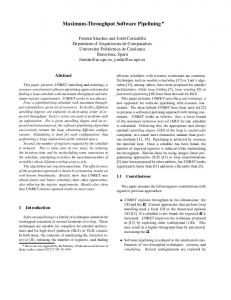
Fig. 2. 7-bit Guild multiplier. Equitemporal lines shown.
III. EXPERIMENTAL RESULTS The WP effect on FPGAs was accidentally observed by the authors of this paper during an exploration of the dependence between glitches, logic depth and power consumption in conventional pipelines. During these experiments [26], [27], a fine-grain pipeline multiplier (one LUT between registers) was manually partitioned and placed on an XC3090PC84-100. The routing was done automatically with the default parameters of the tools. After finishing the circuit, all the registers were eliminated using the Xilinx layout editor [25], but their associate LUT in each CLB was maintained (the direct input pin “di” was not used). In this way, a combinational circuit like the original pipeline but with the same number of LUTs (instead of registers) in all paths was obtained. As a result, not only a low-power but also a high-speed prototype was obtained. The Xilinx static timing analyzer showed a delay of 168.6 ns in the longest path, a value that corresponds to a bandwidth close to 6 MHz; however a throughput of 27 MHz was measured. Moreover, an unstable higher band from 34 to 35.6 MHz was also detected and several vectors were correctly multiplied even at 43 MHz. The experiments shows the feasibility of wave pipelining in FPGAs (a possibility that was also mentioned by F. Klass in the 1994 Stanford seminar EE385B) but also led to an XC3000-based pipeline paradox: registers constitute the scaffolding to construct a high-speed block; but if they are removed after the implementation process, the circuit still holds part of its throughput. In this paper, a complete methodology for the construction of WP on the XC4000 series [10] is presented. In all cases, Guild multipliers have been selected as a case-study. This circuit consists of an array of n2 cells composed of an AND gate plus a full-adder. Each of them have 4 inputs and 2 outputs and can be fitted into one CLB. The 7-bit version is shown in Fig.2. Departing from a common equalized datapath, two WP prototypes were constructed and measured using a Xilinx XC4005PC84-6 chip: the first with intentionally skewed clock, and the second with single-phase synchronization. All the layout procedure (partitioning, placement and routing) was performed manually using the Xilinx layout editor [25]. The
4.0
power consumption [W]
equalization strategy was based on the transformation of spatial regularity into delay equalization. First, each array cell was mapped into one CLB. Then, they were placed as similarly as possible to the original topology, in order to take advantage of the uniformity in both the circuit array and the FPGA structure. This method automatically led to a coarse delay balance, but constrained the word length to 7 bits. During the routing process, the main source of unbalance was caused by the different combination of global and local lines in the paths. This problem was solved by assigning the horizontal global wires to long lines. To compensate the delay of long lines, all the local lines were routed through two magicboxes, using a regular pattern of selected segments of around 3ns that was repeated along the array. In this way, a highly equalized layout was created, with a constant 13-LUT logic depth in all paths. The total occupation was 182 CLBs. The maximum unbalance between all the I/O paths, determined using the Xilinx timing analyzer, resulted in less than 2.1 ns, whereas the longest path exhibited a delay of 135.3 ns. Without the WP effect, this value would limit the throughput to below 8 MHz. Unlike conventional pipeline prototypes, in this case most of the path delay (59 %) corresponds to LUTs, a fact that is the key to the low latency of the circuits. The final layout is depicted in Fig. 4. In spite of the transformations accomplished, the similarity to the Guild topology of Fig. 2 is evident. The color of the original picture has been modified in order to show the CLB functions: processing (dark gray), delaying (light gray), and unused (white). From this layout, the two WP versions with different clocking schemes were constructed. The use of FPGAs offered a unique opportunity to perform an accurate comparison between the synchronization schemes: both WP circuits have exactly the same layout, pads, chip sample, PCB, and output loads. For the intentionally skewed clock prototype, the first column of CLBs was used to lag the clock, creating a new path whose delay matched the datapath one. The clock wiring process was performed in two phases, taking full advantage of the reconfiguration features of FPGAs. The first adjustment was made leaving the outputs unregistered, and measuring the relative position of clock edges and data waves using a highspeed oscilloscope. Then, fine tuning was done by increasing or reducing the skewed clock wiring in steps of around 1 ns, until an optimal combination of bandwidth and tolerance to Vcc fluctuations was obtained. After that, the output registers were enabled again by modifying each IOB employing the layout editor. The main problem found was the different rise and fall times of the interconnection resources, which spoiled the delayed clock duty cycle. The best result corresponded to a 14LUT clock path that minimized the weight of the routing delay. Finally, the clock delay chain was ended in a dedicated clock buffer in order to drive the output registers. It was also connected to an output pad to trigger the logic analyzer used to test the prototype. The synchronization path made use of eight extra CLBs. The transformations of the skewed-clock circuit to get the second WP with single-phase clocking were straightforward. The same layout was employed, but the column of CLBs to delay the clock was eliminated. Instead of them, one of the eight FPGA dedicated clock lines was used to control all the I/O registers. All measurements were made using 216 random vectors as well as a set of 16 operands that produce the toggle of almost all the output pins. The second type of data facilitated the
single-phase wave pipeline
3.5 3.0 skewed-clock wave pipeline
2.5 2.0 1.5 1.0
conventional pipeline (logic depth = 1 LUT)
0.5 0.0 0
10
20
30
40
50
60
70
80
90
clock frequency [MHz] Fig. 3: Power consumption versus frequency
detection of phenomena like double-clocking and zero-clocking [28]. The prototypes operated as fast as fine grain pipelines, but using 28 registers instead of 278. Considering the nature of FPGAs, this reduction is not significant in terms of chip size, but definitely affects the latency achieved. The highest operational frequency band (measured) for the single-phase clocked design was between 83 MHz to 85 MHz, a value similar to the obtained using conventional pipelining in the same chip sample. The intentionally skewed clock prototype exhibited a continuous range of operation up to 80 MHz. The circuits ran more than 10 times faster than the value predicted by the timing analyzer tool, whereas the factor between simulation results and the actual frequency of operation was measured for the same chip as 1.3 for non-equalized pipelines. The actual I/O delay resulted in 95 ns. It was measured in a version of the layout with the output registers removed. A maximum of 8 waves running inside the circuit without interference was determined by simultaneously sampling the input vectors and the output results. Therefore, the latency of the prototype is 9 clock cycles if the output registers are included. Considering that, for n=7 bits, the Guild topology has 13 cells in the longest path, and each of them requires one CLB, a fine-grain classic pipeline must have 13 stages to run over 80 MHz. However, the circuit would have a latency of 14 clock cycles. Pipelining every two cells could reduce the latency to 8 clock cycles, but reaching 80 MHz would imply a non-realistic timing budget for the chip selected. Thus, wave pipelining offers the FPGA end-user a unique high-speed low-latency combination. In terms of area, the equalization cost is high taking into account that a hand-made classic pipeline could be fitted in less CLBs (a 13-stage, 7-bit, Guild array requires 278 registers). However, the final number of CLBs in the wave version is a consequence of two choices: regularity and categorical matching. Both strategies simplify the equalization task but require additional logic. In principle, the use of extra routing to balance LUT delays could reduce the number of CLBs occupied even less than the quantity needed by the equivalent classic pipeline. However, an equalization without categorical matching would require a previous characterization of all chip elements to be performed. The analysis of WP in terms of power consumption demonstrates the relationship between low spurious activity and
path balance. For instance, sampling the output at 400 MHz, a maximum of 40 intermediate values between two consecutive results were measured in an equivalent non-equalized combinational array: ten times the number observed in a balanced version with the same logic depth. Thus, the experiments confirm that speed and power consumption are correlated at the implementation level: both conventional and wave pipelining increase the speed and reduce the power simultaneously. However, the wave prototypes consumed a little more than fine-grain pipeline arrays (Fig. 3). The main disadvantage of WP is its strong dependence on power supply voltage variations, especially in the single-phase version. For example, at 84 MHz (the middle of the last frequency band), changes in power supply below 4.88 V or above 5.13 V produced erroneous outputs. On the contrary, the intentionally skewed clock WP was less sensitive to power supply variations. At 80 MHz, it withstood Vcc variations from 4.56 V to 5.5 V (upper voltage was limited to 5.5 V to avoid an excessive power consumption). This tolerance was similar to that observed in equivalent classic pipelines. Previous circuits have been full-manually implemented (partitioning, placement and routing). However, the WP effect was also observed in automatic place and route implementations, whenever the arrays have the same number of LUTs in all paths (this possibility was suggested to the authors by an anonymous reviewer of the FPGA’96 Symposium). This fact can be explained considering that, if the logic depth is high, the path delays are dominated by the LUTs. Although some wires may have a large delay, the sum of the interconnection delays will always be lower than the sum of the LUT ones, considering that an array exhibits a Pareto-Levy distribution of wiring delays [27]. Thus, in some cases, the WP effect can be spontaneously produced in an FPGA. In that situation, the designer must be aware of this possibility in order to correctly interpret the nature of the better performance obtained. To illustrate the magnitude of this problem, a 7-bit combinational Guild multiplier with registered I/O was manually partitioned so that it had 13 LUTs in all its paths. This circuit was automatically placed and routed, using the default options of the tool. The main results were as follows: the longest path delay was 120.9 ns, and the shortest one was 109.4 ns. The circuit worked up to 64 MHz (measured), with five waves inside it: more than seven times the speed predicted by the timing analyzer tool. The highest operation band was very narrow: just 1 MHz. IV. CONCLUSIONS AND FUTURE WORK The feasibility of constructing WPs using LUTs has been demonstrated, and their distinctive characteristic of low-latency, high-throughput and reasonable power consumption (slightly higher than the conventional pipelining one) has been obtained using commercial chips and tools. Additionally, it has been confirmed that the wave pipelining effect can even be achieved using an automatic place and route, as long as the circuit has nearly the same number of LUTs in all paths. Two synchronization alternatives have been explored. Single-phase clocking allows the designer to embed a WP block as part of a synchronous system, but its main disadvantage is the power supply and temperature dependence. Where endurance against environmental variations is a must, an intentionally skewed clocking allows the WP to tolerate similar
power supply variations as the classic pipelines. From the fast prototyping perspective, WPs offer the designer the only alternative for getting high speed (similar to that of fine-grain conventional pipelines), and low latency (similar to that of the combinational version of a given topology). This can help the gap with other relatively faster VLSI technologies to be reduced, when FPGAs are used for chip emulation. In that case, the higher sensitivity of singlephase WPs to temperature, power supply and run-to-run variations is not significant, considering that just one laboratory prototype will be needed. However, the designer must take into account the principal obstacle of single-phase WP: the narrow ranges of valid clock frequencies and the complexity of their prediction from data book information. Designers interested in verifying the feasibility of WP in other FPGA technologies can perform a simple preliminary experiment. First, a set of LUTs must be cascaded in order to implement an 1-bit wide path crossing the chip. Each LUT must be configured as an inverter. After that, using an oscilloscope, the input-output delay can be measured by introducing a lowfrequency square wave. Then, the input frequency must be gradually increased, until its shape at the output pad appears highly distorted. This effect is caused by difference between the rise and fall times of the elements that compose the path. As a consequence, the last frequency value indicates the bandwidth of a perfectly equalized WP in that chip. As a final remark, the efficiency of wave pipelining in FPGAs could be improved by the manufacturer if extra buffers with a delay similar to the LUT were included in future chips. A set of these elements uniformly distributed along the chip would allow the designer to equalize some paths without consuming extra LUTs. This would not only make the circuit faster, but would also reduce the spurious activity, and therefore the power consumption. REFERENCES [1]
L. Cotten, "Circuit Implementation of High-Speed Pipeline Systems", Proc. Fall Joint Computer Conference, pp. 489-504, 1965. [2] T. Hallin and M. Flynn, "Pipeline of Arithmetic Functions", IEEE Trans. on Computer, pp. 880-886, August 1972. [3] J. Deverell, "Pipeline Iterative Arithmetic Arrays", IEEE Trans. on Computers, pp. 317-322, March 1975. [4] R. Jump and S. Ahura, "Effective Pipeline of Digital Systems", IEEE Trans. on Computers, Vol. C-27, No. 9, pp. 855-865, September 1978. [5] C. Hauck, C. Bamji and J. Allen, "The Systematic Exploration of Pipelined Array Multiplier Performance", Proc. ICASSP 85, pp. 1461-1464, New York: IEEE Press, 1985. [6] M. Hatamian and G. Cash, "A 70-MHz 8-bit x 8 bit Parallel Pipelined Multiplier in 2.5-um CMOS", IEEE Journal of SolidState Circuits, Vol. SC-21, No.4, pp. 505-513, August 1986. [7] T. Noll, D. Schmitt, H. Klar and G. Enders, "A Pipelined 330-MHz Multiplier", IEEE Journal of Solid-State Circuits, Vol. SC-21, No. 3, pp. 411-416, June 1986. [8] G. Burrel (Editor), "Crónica de la Técnica", Barcelona: Plaza & Janes Publishers, 1989, pp. 524-525. [9] H. Guild, "Fully Iterative Fast Array for Binary Multiplication and Addition", Electronic Letters, pp. 263, Vol. 5, No. 12, June 1969. [10] Xilinx Inc., "The Programmable Gate Array Data Book", 3rd Edition, San Jose: 1994.
Fig. 4: XC4005 wave pipeline array multiplier layout (intentionally skewed clock version). [11]
S. Anderson, J. Earle, R. Goldschmidt and D. Powers, "The IBM system/360 model 91 floating point execution unit", IBM Journal Res. Development, Vol. 11, pp. 34-53, January 1967. [12] L. Cotten, "Maximum-rate pipeline systems", Proc. Sprint Joint Computer Conference, pp. 581-586, 1969. [13] D. Wong, G. De Micheli and M. Flynn. "Designing HighPerformance Digital Circuits Using Wave Pipelining", VLSI 89, G. Musgrave and U. Lauther (Eds.), pp. 241-252, Elsevier Science Publishers B.V. North Holland, 1990. [14] D. Wong, "Techniques for Designing High-Performance Digital Circuits Using Wave Pipelining", Tech. Rep. No. CLS-TR-92-508, Stanford University, February 1992. [15] W. Burleson, C. Lee and E. Tan, "A 150 MHz Wave Pipelined Adaptive Digital Filter in 2µ CMOS", VLSI Signal Proc. VII, pp. 296-305, Ed.: J. Rabaey, New York: IEEE Press, 1994. [16] W. Liu, T. Gray, D. Fan, W. Farlow and T. Hughes, "A 250-MHz Wave Pipelined Adder in 2-µm CMOS", IEEE Journal of Solid-State Circuits, Vol. 29, No. 9, pp. 1117-1127, September 1994. [17] K. Nowka and M. Flynn, "Wave Pipelining of High Performance CMOS Static RAM", Tech.Rep. No. CLS-TR-94-615, Stanford University, January 1994. [18] D. Ghosh and S. Nandy, "Design and Realization of HighPerformance Wave-Pipelined 8x8 Multiplier in CMOS Technology", IEEE Trans. on VLSI Systems, Vol. 3, No. 1, pp. 3648, March 1995. [19] F. Klass and M. Flynn, "A 16x16-bit Static CMOS Wave-Pipelined
[20]
[21] [22]
[23]
[24] [25] [26]
[27]
[28]
Multiplier", Proc. ISCAS 94, pp. 143-146, IEEE Press 1994. M. Flynn, K. Nowka, G. Bewick, E. Schwarz and N. Quach, "The SNAP Project: Towards Sub-Nanosecond Arithmetic", Proc. 12th Symposium on Computer Arithmetic, pp. 75-82, IEEE Press 1995. C. Gray, W. Liu and R. Cavin, "Wave Pipelining: Theory and CMOS Implementation", Kluwer Academic Publishers, 1994. C. Chang, E. Davidson and K. Sakallah, “Maximum Rate SinglePhase Clocking of a Closed Pipeline including Wave Pipelining, Stopability and Startability”, IEEE Trans. on CAD of IC and Systems, Vol. 14, No. 12, pp. 1526-1545, December 1995. W. Lam, R. Brayton, A. Sangiovanni-Vicentinelli, “Valid Clock Frequencies and Their Computation in Wavepipelined Circuits”, IEEE Trans. on CAD of IC and Systems, Vol. 15, No. 7, pp. 791807, July 1996. “The Tilde De-Mystified”, in The Programmable Logic Array Data Book, Second Edition, Xilinx Inc., 1994, pp. 9.3. Xilinx Inc., “XACT Reference Manual”, San Jose: 1995. E. Boemo, S. Lopez-Buedo, G. Gonzalez de Rivera, and J. Meneses, "On the Usefulness of Pipelining and Wave Pipelining as LowPower Design Technique", Proc. PATMOS´95 Fifth Int. Workshop, pp. 252-263, Oldenburg: OFFIS, October 1995. E. Boemo, “Contribución al Diseño de Arrays VLSI con Paralelismo de Grano Fino”, Ph.D. Thesis, School of Telecommunication Engineering, Technical University of Madrid, January 1996. http://www.ii.uam.es/~ivan/papers.htm. J. Fishburn, "Clock Skew Optimization", IEEE Trans. on Computers, Vol. 39, No. 7, pp. 945-951, July 1990.