40
IEEE TRANSACTIONS ON NANOTECHNOLOGY, VOL. 4, NO. 1, JANUARY 2005
Spin Injection in Spin FETs Using a Step-Doping Profile Min Shen, Student Member, IEEE, Semion Saikin, and Ming-Cheng Cheng, Senior Member, IEEE
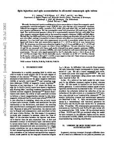
Abstract—We investigate the effect of a step-doping profile on the spin injection from a ferromagnetic metal contact into a semiconductor quantum well in spin field-effect transistors using a Monte Carlo model. The considered scheme uses a heavily doped layer at the metal–semiconductor interface to vary the Schottky barrier shape and enhance the tunneling current. It is found that spin flux (spin current density) is enhanced proportionally to the total current, and the variation of current spin polarization does not exceed 20%. Index Terms—Injection, Schottky barrier, spin, spin field-effect transistor (FET), spintronics. Fig. 1. Spin-FET structure. The n layer at the Fe/GaAs interface is used to vary the shape of the Schottky barrier. w is the width of the high doping layer.
I. INTRODUCTION
U
TILIZATION of the electron spin as an information carrier in conventional semiconductor electronic devices results in a promising idea for semiconductor spintronics [1]–[4]. Different types of spin field-effet transistors (FETs) [5]–[7] and bipolar spin-transistors [8]–[10] have been proposed. However, study of these devices is still at the early stage of development. One of the most challenging problems of semiconductor spintronics is to produce spin-polarized currents in nonmagnetic semiconductor structures. The conventional model of the spin injection from a ferromagnetic contact [11] utilized in metal spintronics [1] is complicated by strong conductance mismatch between the metal and semiconductor [12]. Injection through a tunneling barrier at the ferromagnetic metal/semiconductor interface has been suggested to resolve this problem [13]. Promising results of spin injection through different types of barriers have been reported recently [14]–[16]. In this paper, we study the effect of a step-doping layer at the interface on spin injection through a Schottky barrier into a semiconductor quantum well (QW). The design of spintronic devices requires an appropriate shape of the Schottky barrier to achieve high spin injection. This can be realized by careful selection of material properties Manuscript received May 14, 2004; revised July 5, 2004. This work was supported in part by the National Security Agency and Advanced Research and Development Activity under Army Research Office Contract DAAD-19-02-1-0035 and in part by the National Science Foundation under Grant DMR-0121146. This paper is based on work presented at the 2004 IEEE NTC Quantum Device Technology Workshop. M. Shen and M.-C. Cheng are with the Center for Quantum Device Technology and the Department of Electrical and Computer Engineering, Clarkson University, Potsdam, NY 13699 USA (e-mail:
[email protected];
[email protected]). S. Saikin is with the Center for Quantum Device Technology and the Department of Electrical and Computer Engineering, Clarkson University, Potsdam, NY 13699 USA and also with the Physics Department, Kazan State University, Kazan 420008, Russia (e-mail:
[email protected]). Digital Object Identifier 10.1109/TNANO.2004.840150
and variation of the doping profile to effectively control the spin-polarized current. For spin injection through a Schottky barrier, it was reported that the depletion region is detrimental due to a strong and fast space-varying electric field [17]. However, this effect can be minimized by one of the schemes using barrier engineering [18], which is to use a high doping layer at the metal/semiconductor interface [16]. Efficient spin injection through a tailored Schottky barrier into a bulk semiconductor has been reported in [15] and [16]. In order to reveal and understand the effect of the step doping on spin injection, we apply the previously developed Monte Carlo scheme [19], which was used to study the spin injection through a Schottky barrier with a fixed doping profile. In this paper, we discuss the effect of barrier shape variation introduced by an additional heavily doped layer with m at the metal/semiconductor interface, as shown in the spin-FET structure given in Fig. 1, similar to the spin FET proposed by Datta and Das [5]. Ferromagnetic metal, Fe, is used as the source contact, and the device channel is a QW of Al Ga As/GaAs/Al Ga As heterostructure. Heavily m . doped bulk GaAs is used in the drain with This study focuses on the effect of the high doping layer at the metal/semiconductor interface on the spin injection. Collection of electrons in the drain is assumed to be spin-independent. II. MODEL The Monte Carlo model, described in [19], takes into account thermionic emission and the tunneling mechanism from metal to semiconductor and from semiconductor to metal. The barrier height is assumed to be 0.72 eV [20] and bias-independent. The QW depth is approximately 0.35 eV,1 and the QW width is 10 nm. 1[Online]. bandstr.html
1536-125X/$20.00 © 2005 IEEE
Available:
www.ioffe.rssi.ru/SVA/NSM/Semicond/AlGaAs/
SHEN et al.: SPIN INJECTION IN SPIN FETS USING STEP-DOPING PROFILE
41
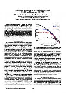
Both Rashba [21] and Dresselhaus [22] effects are included in the spin orbit interaction, which are described by (1) and (2) respectively. and are Rashba and Dresselhaus spin-orbit coupling coefficients, respectively. For GaAs, we use the calculated eV [23], while eV is comvalue, parable with the measured value [24]. In (1) and (2), the coordinate system coincides with the principal crystal axes. The single-electron density matrix is used to describe spin evolution. The evolution of spin density matrix is performed as (3) Fig. 2. Schottky barrier profiles for different widths of the heavily doped layer.
where (4) To describe the spin injection, we use spin current density (or spin flux) defined as (5)
where is the -component velocity of the th is the Pauli matrix. Effect of the spin-orbit splitelectron and ting on the wave vector is assumed to be negligible. In the spin-independent case, the - relation then reduces to the conventional one. If only the linear spin orbit interaction in momentum is included in (1) and (2), it is similar to the - relation [25]. If the cubic terms in the Dresselhaus interaction are taken into account in (2), this approximation ignores the broadening of the single-electron wave packet. For spin-polarized currents (but not for pure spin currents [26], [27]), the normalized current spin polarization
(6) can be introduced, where is the -component of the total current density. In general, this characteristic of current spin polarization differs from the particle spin polarization used in [28] and [29]. We found it to be useful for studying spin dynamics. In the following text, we discuss the spin-polarized current along the external electric field applied in the direction. Therefore, the notations for spin current density, total current density, and current spin polarization are simplified as , , , respectively. For absolute values, we use and and . Because a total spin in the system with spin-orbit interaction is not conserved, spin current and spin current polarization are coordinate-dependent.
Fig. 3. Electron concentrations for different widths of the heavily doped layer.
III. SIMULATION RESULTS AND DISCUSSION Simulations are performed at room temperature in the struc0, 15, 25, 45, and 95 nm at the ture given in Fig. 1 with 0.1 V. The barrier profiles and elecsource–drain voltage tron concentrations for five different widths of the high doping layer, determined from the self-consistent solution of Poisson equation and electron motion, are shown in Figs. 2 and 3. This naturally incorporates effects of inhomogeneous doping on spin dynamics [30]. Inclusion of the heavily doped layer at the contact interface narrows the barrier width. However, the decrease 30 nm. It in the barrier width with becomes saturated at should be mentioned that Fig. 2 shows the conduction band pro200 nm, while the channel files only in the region of 0 700 nm, as displayed in Fig. 1. Though in the extends to channel the conduction band profiles vary with , as shown in Fig. 2, these band energies derived from different values of eventually converge to the same value at the n drain.
42
IEEE TRANSACTIONS ON NANOTECHNOLOGY, VOL. 4, NO. 1, JANUARY 2005
Fig. 4. Distribution of the injection rate versus energy for different widths of the heavily doped layer.
Fig. 4 shows the influence of the change in the barrier profile on the energy distribution of the injected electrons. The distribution at the higher energy edge is controlled by the barrier height (i.e., dominated by the thermionic emission), while the distribution at the lower energy edge is influenced by the tunneling efficiency. The area under the distribution reflects the injection strength. According to Fig. 4, introduction of the interface step-doping layer increases the injection strength. In addition, the threshold energy level for the evident injection rapidly decreases with the layer width , as increase from 0.1 V, the threshold en0. At the considered bias, ergy reach however a minimum level near 0.1 eV for 25 nm. Fig. 2 shows that the conduction band energy decreases rapidly with near the Schottky contact, especially . The grid size m used in the simfor ulation does not provide enough spatial resolution near the contact. It is believed that the insufficient spatial resolution leads to a tunneling probability which approximately increases exponentially with energy and compensates the exponentially decreasing Maxwellian distribution function of electrons in the metal. As a result, a nearly constant energy distribution of the injection rate is observed within the energy range where the spatial resolution is insufficient. Fig. 5(a) and (b) shows three components of the spin flux for the spin injection in the structure without the interface stepdoping layer . Injected electrons are 100% spin polarized in the and orientations. Both linear and nonlinear spin orbit interactions, given in (1) and (2), are included. This case is used as the reference to study effects of the barrier profile on spin dynamics. The current spin polarizations defined in (6) are illustrated in Fig. 6(a) and (b), corresponding to the cases presented in Fig. 5(a) and (b), respectively. Results accounting for only linear spin orbit interaction are also displayed in Fig. 6(a) and (b) as solid lines. In this case, the small difference in the spin-polarization profiles along the channel for different polarizations of injected electrons results from the anisotropy of spin relaxation rates in semiconductor heterostructures [28], [31]. Although in
Fig. 5. Three components of spin flux with spin-polarized injection (a) in the x orientation and (b) in the y orientation.
most studies of spin FETs only the linear spin-orbit terms are included, Fig. 6 shows that, in the considered structure, current spin polarization is strongly influenced by the nonlinear Dresselhaus term. The current spin component in the channel direction decays on a length scale of 0.1 m when the nonlinear term is included, though the component of the current spin polarization relaxes appreciably more slowly. We attribute this strong anisotropy of spin dynamics to the velocity distribution of the injected electrons rather than the interplay of the Rashba and Dresselhaus coefficients. Our following discussion regarding the width of the stepdoping effect will be focused on the injection spin polarization in the direction in which spin polarization is conserved in a much longer length scale. The interface doping tailors the barrier profile that induces the following effects: 1) change in the tunneling probability and thus tunneling current; 2) modification of the energy distribution of the injected particles, which influences spin dynamics in the channel; 3) change in the initial distribution of spin polarization in the case of non-100% spin-polarized injection. Attempts are made to analyze these three effects separately. Fig. 7 shows the ratio of the injected current density in the channel in the case with a step-doping layer to that with no step doping (the reference case shown in Fig. 5) as a function of the layer width. The absolute value of the maximum variation for the current spin polarization induced by the various widths of
SHEN et al.: SPIN INJECTION IN SPIN FETS USING STEP-DOPING PROFILE
43
Fig. 8. Shifted variation of the current spin polarization in the channel direction.
Fig. 6. Current spin polarization with spin-polarized injection (a) in the x orientation and (b) in the y orientation.
doping layer width due to the enhancement of total current density. The current density (therefore the spin current density) is for 25 nm, as shown in exponentially dependent on Fig. 7. The ratio is saturated for 30 nm, which is consistent with the saturation of the barrier thinning shown in Fig. 3. The above discussion is based on a 100% polarization for the injected electrons. Realistically, electrons are injected from the that is ferromagnetic contact with a certain polarization dependent on electron energy , material parameters, and interface quality. It can be derived based on first principle calculations [32]. For simplicity, to check the effect of the initial polarization on the spin dynamics in the device, we approximate by the ratio of densities of states between the majority and minority spins in the metal contact [19]. Fig. 8 presents the deviation of the absolute percentage variation for the current spin polarization due to the non-100% spin-polarized injection with respect to the reference case (100% spin polarization). In both 15 nm. The injection efficiency with respect to the cases, , and the variation reference case shifted to along the device channel is about 8%. This indicates that effects , and the barrier profile on spin of the initial polarization polarized current are nearly separable. There are other parameters, such as the step-doping density and the barrier height, that can be adjusted to improve the results. This will be studied in the near future. IV. CONCLUSION
Fig. 7. Ratio of total injected current density in the channel direction for the case with the high doping layer to the reference case (no doping layer) versus the layer width. The absolute value of the maximum variation of the current spin polarization (caused by the doped layer of various widths) with respect to the reference case is shown in the inset.
the step-doping layer with respect to the reference case is shown in the inset, where
changes from 2.5% up to 20% of the total polarization along the channel. The effect of different widths of the step-doping layer on the current polarization actually does not exceed 20%. However, the spin current strongly depends on the
We study the effect of different widths of the step-doping layer at the metal–semiconductor interface on the spin injection in spin FETs. The Monte Carlo simulation results indicate that the higher order spin-orbit term plays an important role in spin injection transport. It is found that spin flux (spin current density) is enhanced exponentially by an increase in the width of the step doping at the contact–semiconductor interface for 25 nm and becomes saturated for 30 nm. The influence of the width variation of the high step-doping layer on the current spin polarization actually does not exceed 20%. ACKNOWLEDGMENT The authors would like to thank Prof. V. Privman for valuable discussions.
44
IEEE TRANSACTIONS ON NANOTECHNOLOGY, VOL. 4, NO. 1, JANUARY 2005
REFERENCES [1] S. A. Wolf, D. D. Awschalom, R. A. Buhrman, J. M. Daughton, S. von Molnar, M. L. Roukes, A. Y. Chtchelkanova, and D. M. Treger, “Spintronics: A spin-based electronics vision for the future,” Science, vol. 294, pp. 1488–1495, 2001. [2] I. Zutic, J. Fabian, and S. D. Sarma, “Spintronics: Fundamentals and applications,” Rev. Modern Phys., vol. 76, pp. 323–410, 2004. [3] D. D. Awschalom, M. E. Flatte, and N. Samarth, “Spintronics,” Sci. Amer., vol. 286, no. 6, pp. 66–73, 2002. [4] H. Akinaga and H. Ohno, “Semiconductor spintronics,” IEEE Trans. Nanotechnol., vol. 1, pp. 19–31, Jan. 2002. [5] S. Datta and B. Das, “Electronic analog of the electro-optic modulator,” Appl. Phys. Lett., vol. 56, pp. 665–667, 1990. [6] J. Schliemann, J. C. Egues, and D. Loss, “Non-ballistic spin-field-effect transistor,” Phys. Rev. Lett., vol. 90, 2003. [7] J. C. Egues, G. Burkard, and D. Loss, “Datta-Das transistor with enhanced spin control,” Appl. Phys. Lett., vol. 82, pp. 2658–2660, 2003. [8] J. Fabian, I. Zutic, and S. D. Sarma, “Theory of spin-polarized bipolar transport in magnetic p-n junctions,” Phys. Rev. B, Condens. Matter, vol. 66, 2002, art. no. 165301. [9] M. E. Flatte, Z. G. Yu, E. Johnson-Halperin, and D. D. Awschalom, “Theory of semiconductor magnetic bipolar transistors,” Appl. Phys. Lett., vol. 82, pp. 4740–4742, 2003. [10] J. Fabian, I. Zutic, and S. D. Sarma, “Magnetic bipolar transistor,” Appl. Phys. Lett., vol. 84, pp. 85–87, 2004. [11] P. R. Hammar, B. R. Bennett, M. J. Yang, and M. Johnson, “Observation of spin injection at a ferromagnet-semiconductor interface,” Phys. Rev. Lett., vol. 83, pp. 203–206, 1999. [12] G. Schmidt, D. Ferrand, L. W. Molenkamp, A. T. Filip, and B. J. van Wees, “Fundamental obstacle for electrical spin injection from a ferromagnetic metal into a diffusive semiconductor,” Phys. Rev. B, Condens. Matter, vol. 62, pp. R4790–R4793, 2000. [13] E. I. Rashba, “Theory of electrical spin injection: Tunnel contacts as a solution of the conductivity mismatch problem,” Phys. Rev. B, Condens. Matter, vol. 62, pp. R16267–R16270, 2000. [14] K. H. Ploog, “Spin injection ferromagnet-semiconductor heterostructures at room temperature,” J. Appl. Phys., vol. 91, pp. 7256–7260, 2002. [15] V. F. Motsnyi, J. De Boeck, J. Das, W. Van Roy, G. Borghs, E. Goovaerts, and V. I. Safarov, “Electrical spin injection in a ferromagnet/ tunnel barrier/semiconductor heterostructure,” Appl. Phys. Lett., vol. 81, pp. 265–267, 2002. [16] A. T. Hanbicki, O. M. J. van’t Erve, R. Magno, G. Kioseoglou, C. H. Li, B. T. Jonker, G. Itskos, R. Mallory, M. Yasar, and A. Petrou, “Analysis of the transport process providing spin injection through an Fe/AlGaAs Schottky barrier,” App. Phys. Lett., vol. 82, pp. 4092–4094, 2003. [17] J. D. Albrecht and D. L. Smith, “Electron spin injection at a Schottky contact,” Phys. Rev. B, Condens. Matter, vol. 66, 2002, art. no. 113303. [18] S. Sassen, B. Witzigmann, C. Wolk, and H. Brugger, “Barrier height engineering on GaAs THz Schottky diodes by means of high-low doping, InGaAs- and InGaP-layers,” IEEE Trans. Electron Devices, vol. 47, pp. 24–32, 2000. [19] M. Shen, S. Saikin, and M.-C. Cheng, “Monte Carlo modeling of spin injection through the Schottky barrier and spin transport in a semiconductor quantum well,” J. Appl. Phys., vol. 96, pp. 4319–4325, 2004. [20] J. R. Waldrop, “Schottky barrier height of ideal metal contacts to GaAs,” Appl. Phys. Lett., vol. 44, pp. 1002–1004, 1984. [21] Y. Bychkov and E. I. Rashba, “Oscillatory effects and the magnetic susceptibility of carriers in inversion layers,” J. Phys. C, Solid State Phys., vol. 17, pp. 6039–6045, 1984. [22] G. Dresselhaus, “Spin-orbit coupling effects in Zinc Blende structures,” Phys. Rev., vol. 100, pp. 580–586, 1955. [23] M. Cardona, N. E. Christensen, and G. Fasol, “Relativistic band structure and spin-orbit splitting of Zinc-Blende-type semiconductors,” Phys. Rev. B, Condens. Matter, vol. 38, pp. 1806–1827, 1988. [24] J. B. Miller, D. M. Zumbühl, C. M. Marcus, Y. B. Lyanda-Geller, D. Goldhaber-Gordon, K. Campman, and A. C. Gossard, “Gate-controlled spin-orbit quantum interference effects in lateral transport,” Phys. Rev. Lett., vol. 90, 2003, art. no. 076807. [25] B. S. Pramanik, S. Bandyopadhyay, and M. Cahay, “Decay of spin-polarized hot carrier current in a quasione-dimensional spin-valve structure,” Appl. Phys. Lett., vol. 84, pp. 266–268, 2004. [26] S. Murakami, N. Nagaosa, and S.-C. Zhang, “Dissipationless quantum spin current at room temperature,” Science, vol. 301, pp. 1348–1351, 2003. [27] J. Sinova, D. Culcer, Q. Niu, N. A. Sinitsyn, T. Jungwirth, and A. H. MacDonald, “Universal intrinsic spin Hall effect,” Phys. Rev. Lett., vol. 92, 2004, art. no. 126603. [28] S. Pramanik, S. Bandyopadhyay, and M. Cahay, “Spin dephasing in quantum wires,” Phys. Rev. B, Condens. Matter, vol. 68, 2003, art. no. 075313.
[29] S. Saikin, M. Shen, M.-C. Cheng, and V. Privman, “Semiclassical Monte Carlo model for in-plane transport of spin-polarized electrons in III–V heterostructures,” J. Appl. Phys., vol. 94, pp. 1769–1775, 2003. [30] Y. V. Pershin and V. Privman, “Focusing of spin polarization in semiconductors by inhomogeneous doping,” Phys. Rev. Lett., vol. 90, 2003, art. no. 256602. [31] K. M. I. Dyakonov and V. Y. Kachorovskii, “Spin relaxation of two-dimensional electrons in noncentrosymmertic semiconductors,” Sov. Phys. Semicond., vol. 20, pp. 110–112, 1986. [32] X.-G. Zhang and W. H. Butler, “Band structure, evanescent states, and transport in spin tunnel junctions,” J. Phys., vol. 15, pp. R1603–R1639, 2003.
Min Shen (S’04) was born in Shanghai, China. He received the B.S. degree in electrical engineering and the M.S. degree in fluid mechanics from Shanghai University of Technology (now Shanghai University), Shanghai, China, in 1982 and 1987, respectively. He is currently working toward the Ph.D. degree in electrical engineering at Clarkson University, Potsdam, NY. From 1982 to 1984, he was a Lecturer with the Shanghai Polytechnic School of Electronic Instruments, Shanghai, China. From 1987 to 1998, he was with the Institute of Applied Mathematics and Mechanics, Shanghai University. From 1998 to 2000, he was a Visiting Scholar with the Advanced Material Research Institute, University of New Orleans, New Orleans, LA. From 2000 to 2001, he was with Celestica International, Inc., Toronto, ON, Canada. He joined Clarkson University, Potsdam, NY, as a Research Assistant in 2002. His research interests include modeling and simulation of nanoscale electronic and spintronic devices, transient heat flow models of SOI devices, heat and mass transfer in engineering processes, and computational fluid dynamics. Mr. Shen coauthored the paper that received the Best Paper Award from the 2003 IEEE Conference on Electron Devices and Solid-State Circuits (EDSSC).
Semion Saikin was born in Kazan, Russia. He received the M.S. degree in physics and the Ph.D. degree in theoretical physics from the Kazan State University, Kazan, Russia, in 1995 and 1998, respectively. Since 1999, he has been an Assistant Professor with the Theoretical Physics Department, Kazan State University. On leave of absence from Kazan State University since 2001, he has been a Research Associate with the Center for Quantum Device Technology, affiliated with the Department of Electrical and Computer Engineering, Clarkson University, Potsdam, NY. His research interests center on the field of solid-state physics with an emphasis on application to modern device technology, including microscopic structure of crystals and evolution of open quantum systems for quantum computation and spintronics application.
Ming-Cheng Cheng (M’90–SM’04) was born in Kaohsiung, Taiwan. He received the B.S. degree in electrophysics from the National Chiao-Tung University, Taiwan, in 1980 and the M.S. degree in systems engineering and the Ph.D. degree in electrical engineering from the Polytechnic University, Brooklyn, NY, in 1986 and 1990, respectively. From 1982 to 1984, he was as an Electronic Engineer with International Telephone and Telegraph (ITT), Taiwan. After receiving the Ph.D. degree, he was with Department of Electrical Engineering, University of New Orleans, New Orleans, LA, from 1990 to 2000. Since 2000, he has been an Associate Professor with the Department of Electrical and Computer Engineering, Clarkson University, Potsdam, NY. He has been involved in transport models for advanced semiconductor devices, optimization of microelectronic devices, and heat flow models for SOI devices and interconnects. His current research interests are in general concerned with simulation and physical modeling of next-generation solid-state devices, including quantum spintronic devices, and compact modeling of heat flow in SOI structures. Dr. Cheng received the Best Paper Award from the 2003 IEEE Conference on Electron Devices and Solid-State Circuits (EDSSC). He is also the recipient of the National Science Foundation Research Initiation Award in 1995 from the Solid State and Microstructures Engineering Program.