Jeffrey W. Elam,. 4. N. J. Zaluzec,. 5. P.F.. Nealey. 1,2. 1. Institute for Molecular Engineering, University of Chicago, Chicago, USA. 2. Materials Science Division ...
611 doi:10.1017/S1431927615003852
Paper No. 0306
Microsc. Microanal. 21 (Suppl 3), 2015 © Microscopy Society of America 2015
Staining Block Copolymers using Sequential Infiltration Synthesis for High Contrast Imaging and STEM tomography T. Segal-Peretz,1,2 J. Winterstein,3 M. Biswas,4 J.A. Liddle,3 Jeffrey W. Elam,4 N. J. Zaluzec,5 P.F. Nealey1,2 1
Institute for Molecular Engineering, University of Chicago, Chicago, USA Materials Science Division, Argonne National Laboratory, Argonne, USA 3 Center for Nanoscale Science and Technology, National Institute of Standards and Technology, Gaithersburg, USA 4 Energy Systems Division, Argonne National Laboratory, Argonne, USA 5 Electron Microscopy Center, NST Division , Argonne National Laboratory, Argonne, USA 2
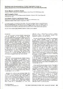
Block copolymers (BCP) are considered promising materials for advanced lithography in the sub-20 nm regime, as well as versatile building blocks for a variety of applications ranging from solar cells to membranes. Since the performance and functionally of BCP films is related to their three dimensional (3D) structure, it is desired to characterize the 3D structure using Transmission Electron Microscopy (TEM) and TEM tomography. A key challenge for TEM imaging of most BCPs is their poor contrast. Therefore, BCPs are routinely stained with conventional staining agents such as OsO4 and I2 to increase their scattering contrast. This staining process can lead to undesired swelling and artifacts.1 Figure 1 shows a comparison of annular dark field (ADF) scanning transmission electron microscopy (STEM) imaging of cylinder-forming and lamellae-forming poly(styrene-block-methyl methacrylate) (PS-b-PMMA) BCP films prior to any staining, and after staining with Al2O3 using sequential infiltration synthesis (SIS). SIS is an emerging technique for growing inorganic materials in polymer and block copolymer films using an atomic layer deposition tool.2 The inorganic material is grown in a block-selective manner within the polar domains of the BCP. During the SIS process, one of the precursors (trimethyl-aluminum) selectively interact with the polar moieties (carbonyl groups), resulting in Al2O3 growth that occurs predominantly in the PMMA domains, as can be seen in the x-ray energy dispersive spectropy (XEDS) STEM mapping of lamellae-forming PS-PMMA film (Figure 2). The introduction of Al2O3 significantly enhances the high-angle scattering from the polar domains, and enables high contrast imaging in ADF-STEM mode (Figures 1 and 2). The enhanced contrast of SIS-treated films under ADF-STEM conditions enables 3D characterization of PS-b-PMMA BCP films using STEM tomography. By tuning the SIS conditions, the Al2O3 can serve as a staining agent with high fidelity to the BCP domains, enabling detailed investigation of the 3D structure. For example, ADF-STEM tomography of cylinder-forming PS-b-PMMA film with perpendicular orientation (Figure 3), revealed the morphology of individual domains across the film’s depth, defects in the self-assembled film, and grain boundaries. Typical dislocation defects are observed at the grain boundaries of the film. While most of the dislocations persist the entire film’s depth, splitting dislocation, were also observed (Figures 3d and 3e), where a single cylinder splits into two cylinders towards the bottom of the film. Combining SIS and ADF-STEM tomography opens a window for studying the 3D structure of BCPs with high precision, leading to better understanding of their behavior. References: [1] Staniewicz L. et al., J. Phys.: Conference Series (2010), 012077 [2] Peng Q., Tsemg Y. C. and Elam J. W., Adv. Mater. 22 (2010), 5129.
Microsc. Microanal. 21 (Suppl 3), 2015
612
[3] This work was supported by U.S. Department of Energy, Office of Science, Office of Basic Energy Sciences, under Contract No. DE-AC02-06CH11357.
Figure 1: STEM images of as prepared film (a),(b), and after three cycles of Al2O3 SIS (c),(d), of cylinder-forming PS-PMMA (a),(c), and lamellae-forming PS-PMMA (b)(d). Film thicknesses are 50 nm and 80 nm, respectively.
Figure 2: XEDS-STEM mapping of lamellaeforming PS-PMMA. (a) ADF-STEM image of lamellae-forming PS-PMMA after three cycles of Al2O3 SIS; (b),(c) are the corresponding elemental mapping of aluminum, and oxygen K x-ray lines, respectively. Scale bars are 50 nm.
Figure 3: ADF-STEM tomography of cylinderforming PS-PMMA films treated with three cycles of Al2O3 SIS: (a) xy slice (parallel to the substrate) of the reconstructed volume taken from the middle of the film. (b) Visualization of the 3D reconstructed volume; film thickness is 50 nm. For clarity PMMA domains are colored in blue while PS domains are transparent. (c) 1.1 nm thick yz digitally sliced cross section of the reconstructed volume taken at the dashed yellow line in (a). (d),(e) yz cross section, and visualization of a splitting dislocation defect formed at grain boundaries of the film shown in (c).