Jan 1, 1987 - J. R. Hayes and A. F. J. Levi, IEEE J. Quantum Electron. QE-22, 1744(1986). M. Heiblum, M. I. Nathan, D. C. Thomas, and C. M. Knoedler, Phys.
SUPERLATTICE TUNNELING DETECTORS OPERATING AT λ = 10 µm, BASED ON QUANTUM WELL INTERSUBBAND ABSORPTION B. Levine, K. Choi, C. Bethea, J. Walker, R. Malik
To cite this version: B. Levine, K. Choi, C. Bethea, J. Walker, R. Malik. SUPERLATTICE TUNNELING DETECTORS OPERATING AT λ = 10 µm, BASED ON QUANTUM WELL INTERSUBBAND ABSORPTION. Journal de Physique Colloques, 1987, 48 (C5), pp.C5-611-C5-614. .
HAL Id: jpa-00226716 https://hal.archives-ouvertes.fr/jpa-00226716 Submitted on 1 Jan 1987
HAL is a multi-disciplinary open access archive for the deposit and dissemination of scientific research documents, whether they are published or not. The documents may come from teaching and research institutions in France or abroad, or from public or private research centers.
L’archive ouverte pluridisciplinaire HAL, est destinée au dépôt et à la diffusion de documents scientifiques de niveau recherche, publiés ou non, émanant des établissements d’enseignement et de recherche français ou étrangers, des laboratoires publics ou privés.
JOURNAL DE PHYSIQUE Colloque C5, suppl6ment au noll, Tome 48, novembre 1987
SUPERLATTICE TUNNELING DETECTORS OPERATING AT QUANTUM WELL INTERSUBBAND ABSORPTION B.F. LEVINE, K.K.
CHOI, C.G.
X
= 10 pm,
BASED ON
BETHEA, J. WALKER and R.J. MALIK
A T and X Bell Laboratories, Murray Hill, NJ 07974, U.S.A.
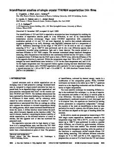
We demonstrate a novel 10.3 p m superlattice infrared detector based o n doped q u a n t u m wells of GaAs/AlGaAs. Intersubband resonance radiation excites an electron from t h e ground s t a t e into the first excited s t a t e , where it rapidly tunnels o u t producing a photocurrent. W e achieve a narrow bandwidth (10%) photosensitivity with a responsivity a s large as 1.9 A / W and an estimated speed of 30 ps. ~ e c e n t l ~we ' have demonstrated t h e first 10pm infrared detector based on a superlattice of doped GaAs/AlGaAs q u a n t u m wells. T h e motivation for this work is t h a t t h e fabrication of 10pm infrared detectors from 111-V materials would allow advantageous use of their more highly developed growth and processing technologies, as compared with 11-VI ~ o m ~ o u n d s ~F-u~r t.h e r more, device parameters (e.g. band gap, operating temperature, bandwidth , and speed) can be tailored in ways t h a t are difficult t o do with either 11-VI's o r extrinsic S i detectors. W e report here t h e demonstration of a novel high-speed infrared detector based on intersubband absorption and sequential resonant tunneling in doped Gaks/AI,Gal-,As quantum welt superlattices. W e achieved a responsivity as large a s 1.9 AJW a t A = 10.3 p m , a narrow bandwidth response of A X/X = lo%, and estimate t h e speed t o be z 30 ps. From our experiments we have d e t e r ~ i n e d t h a t the mean free p a t h of t h e photogenerated h o t electrons through t h e superlattice is 4500 A. In order t o understand the operation of this detector it is useful t o first discuss tunneling5-' and intersubband absorptiong-'' in doped superlattices T h e infiared radiation is in a superlattice of doped absorbed via t h e q u a n t u m well intersubband resonanceg-'' Ga.4s/AIxGal-,As quantum wells and t h e photoexcited electrons rapidly tunnel o u t of t h e well, thereby producing a photocurrent. W e have studied in detail8 t h e transport characteristics of these weakly coupled GaAs-GaAIAs multiquantum wells and concluded t h a t t h e stair-like potential profile as shown in Fig. ( l a )
Fig. 1 (a) Sequential resonant tunneling in high field domain (right-hand side): tunneling through ground s t a t e (left-hand side). (b) Photoconductivity produced by absorption of intersubband radiation followed by tunneling o u t of well.
Article published online by EDP Sciences and available at http://dx.doi.org/10.1051/jphyscol:19875131
JOURNAL DE PHYSIQUE
C5-612
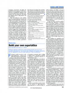
is the stable configuration when t h e applied bia voltage CV,)is less t h a n m(E2-El), where m is the number of periods of in t h e structure, and El and E2 are t h e energies of t h e ground and t h e first excited s t a t e s in t h e wells respectively. A t low temperatures without infrared radiation, electric conduction is via sequential resonant tunneling either between t h e ground s t a t e s of each well or between t h e ground s t a t e s and t h e first excited s t a t e s of,the adjacent wells, depending on t h e is incident on t h e sample, voltage drop across t h e period. When infrared energy equal electrons are excited t o t h e first excited s t a t e , producing hot electrons after tunneling o u t of t h e wells (see Fig. (lb). Sin& t h e mobility of t h e hot electrons is different from those in t h e wells, a change of conductance is expected. W e named this device a STAIR detector (an acronym for Superlattice Tunneling and Absorption by Intersubband Resonance detector and also because of the stair-like band configuration). In order t o t e s t t h e dependence of the photeexcited tunneling on t h e height and thicktunneling barriers two samples were grown and measured. Sample A conness of t h e A1,Gal-,As sist$d of a 50 period sliperlattice of 65 A GaAs wells (doped 1 . 4 ~ 1 0 ' ~ c r n - ~an$ 95A Ale 2sGao75AS barriers, sandwiched between highly doped contact layers; sample B had 7 0 A quantum wells and 140 A A l o , 3 6 G ~ . s 4 A Sbarriers. These thicknesses and compositions were chosen t o produce only two s t a t e s in the well with an energy spacing close t o 1 0 p m . In crder t o measure the resonance energy and oscillator strength we ~ e r f o r m e dFourier transform interferometer absorption measurementsg-lo with t h e crystal a t Brewster's angle Ob=73', since t h e polarization selection rule of this transition requires t h e optical electric field t o have a component perpen dicular t o the superlattice. T h e absorption of sample A (Fig. 2) is peaked a t 920'cm-' with a full width a t half-maximum of ~ v = 9 7 c m - l corresponding t o an excited s t a t e lifetime of T2= (ii~v)-1=1.1x10⁻¹³s(110fs). T h e peak absorbance A = -log (transmission) = 2 . 2 ~ 1 0 - ~ corresponds t o an oscillator s t r e r ~ g t h ~of- ~f=0.6 ~ in good agreement with o u r theoretical value f=0.8. In order t o measure t h e infrared photoconductivity a detector was fabricated by etching a 5 0 p m - d i a m mesa and making Ohmic contact t o t h e top and bottom nt -GaAs layers. In addition, a 45' angle was polished on t h e substrate (see insert in Fig. 2) to allow t h e infrared light t o back illuminate t h e detector a t a 45' angle of incidence.
to$^^-^^
T h i s allows for a large optical field normal t o the superlattice. T h e strongly resonant character of the photocurrent (Fig. 2) is in close agreement with the measured absorption spectrum: Furthermore, a s expected, t h e photosignal was determined t o be highly polarized with t h e optical transition dipole moment aligned normal t o t h e superlattice. T h e responsivity R of Sample A increased with bias, reaching a maximum value of R=0.5 A/W a t a bias of 2.6V, corresponding t o a quantum efficiency of 6%. By fitting this d a t a (shown in Fig. 3)
R(OTUSR(SITIVE LENGTH
f (PERIQOSI
PHOTON ENERGY [cm"l
Fig. 3 Solid points are measured responsivity Fig. 2 Curve is measured absorption spectrum for Sample A; solid points are photocurrent vs. photon energy (normalized t o the peak absorbance); insert shows device geometry
R vs. the photosensitive length 1 of t h e high field domain for Sample A; t h e curve is theory including t h e hot electron mean free path L.
with a theoretical calculation1 which includes t h e responsivity dependence o n t h e photoexcited tunneling probability a n a t h e m$an free path L we can determine both of these quantities. T h e result is p=60% and L=2500 A. This value for L is much longer t h a n a ballistic mean free path12~13due t o the rapid potential drop produced by the resonant alignment of El and E2. If we a t t e m p t t o increase t h e responsivity further in Sample A by increasing t h e bias V, the d a r k current rapidly increases. However, due t o the thicker tunneling banners in Sample B, t h e dark current is several orders of magnitude lower for t h e same bias and hence t h e voltage can then be increased further, thereby increasing the photoexcited tunneling probability and photocurrent. A t Va=9V, we achieve a high responsivity of R=l.SA/W, (which is $early four times larger than for Sample A) and a long hot electron mean free p a t h of L= 4500A, a t Va=3.4V (nearly twice as large as Sample A). F o r biases larger than 3.4V, t h e mean free p a t h , L, rapidly increases s o t h a t t h e effective photoconductive transport distance, becomes the total superlattice thickness. W e have developed a detailed theory of t h e intersubband absorption, photoexcited tunneling and hot electron transport through these multiquantum well superlattices. A s shown in Fig. 4 o u r calculations are in good agreement with experiment over 3 orders of magnitude in responsivity. F r o m this d a t a we can also estimate the electron velocity and hence estimate the response speed t o be very fast (30 psec). In conclusion we have demonstrated a new concept in long wavelength infrared detec= tors, a n d achieved a high responsivity R=l.SA/W, an advantageous narrow bandwidth (A lo%), : and a very high estimated response speed (30 psec).
Fig. 4 T h e voltage dependence of t h e dark current and t h e responsivity of Sample B. T h e dashed curve is the theoretical fitting t o the responsivity.
REFERENCES [I] B. F. Levine, K . K. Choi, C. G. Bethea, J. Walker and R. J. Malik, Appl. Phys. L e t t 50, 1092(1987). [2] J. S . Smith, L. C . Chiu, S. Margalit, A. Yariv, and A. Y. Cho, J. Vac, Sci. Technol. B 1, 37 6(1983)
(31 D. D. Coon and R. P. G. Karunasiri, Appl. Phys. Lett. 45, 649(1984). 141 F. Capasso, K. Mohammed, a n d A. Y. Cho, IEEE J. Quantum Electron. QE-22, 1853(1986). 151 L. Esaki and L. L. Chang, Phys. Rev. Lett. 33, 495(1974)
C5-614
JOURNAL DE PHYSIQUE
Y. ICawamura, K. W a k i t a , H. Asahi, and I