Switching teraherz waves with gate-controlled active graphene metamaterials Seung Hoon Lee1*, Muhan Choi2*, Teun-Teun Kim1*, Seungwoo Lee1, Ming Liu3, Xiaobo Yin3, Hong Kyw Choi2, Seung S. Lee1, Choon-Gi Choi2, Sung-Yool Choi4, Xiang Zhang3,5 & Bumki Min1 1
Department of Mechanical Engineering, Korea Advanced Institute of Science and
Technology (KAIST), Daejeon 305-751, Republic of Korea 2
Creative Research Center for Graphene Electronics, Electronics and
Telecommunications Research Institute (ETRI), Daejeon 305-700, Republic of Korea 3
Nanoscale Science and Engineering Center, 3112 Etcheverry Hall, University of
California, Berkeley, California 94720, USA 4
Department of Electrical Engineering, Korea Advanced Institute of Science and
Technology (KAIST), Daejeon 305-751, Republic of Korea 5
Material Science Division, Lawrence Berkeley National Laboratory, 1 Cyclotron Road,
Berkeley, California 94720, USA *
These authors contribute equally to this work.
The extraordinary electronic properties of graphene, such as its continuously gatevariable ambipolar field effect and the resulting steep change in resistivity, provided the main thrusts for the rapid advance of graphene electronics1.
The gate-
controllable electronic properties of graphene provide a route to efficiently 1
manipulate the interaction of low-energy photons with massless Dirac fermions, which has recently sparked keen interest in graphene plasmonics2-10. However, the electro-optic tuning capability of unpatterned graphene alone is still not strong enough for practical optoelectronic applications due to its nonresonant Drude-like behaviour.
Here, we experimentally demonstrate that substantial gate-induced
persistent switching and linear modulation of terahertz waves can be achieved in a two-dimensional artificial material, referred to as a metamaterial11,12, into which an atomically thin, gated two-dimensional graphene layer is integrated. The gatecontrollable light-matter interaction in the graphene layer can be greatly enhanced by the strong resonances and the corresponding field enhancement in the metamaterial13. Although the thickness of the embedded single-layer graphene is more than ‘six’ orders of magnitude smaller than the wavelength (< λ/1,000,000), the one-atom-thick layer, in conjunction with the metamaterial, can modulate both the amplitude of the transmitted wave by up to 90 per cent and its phase by more than 40 degrees at room temperature. More interestingly, the gate-controlled active graphene metamaterials show hysteretic behaviour in the transmission of terahertz waves, especially when fabricated with multilayer graphene, which is indicative of persistent photonic memory effects. The controllable light-matter interaction, as well as the memory effect in the active graphene metamaterials, present immense potential for a myriad of important applications, particularly in active control of terahertz waves in the extreme subwavelength-scale, such as fast terahertz modulators, tunable transformation-optics devices, electrically controllable photonic memory, and reconfigurable terahertz devices. 2
Terahertz frequencies are situated in the far-infrared spectra of electromagnetic radiation that inherit the richness of photonics and electronics, as well as their weaknesses14,15. The development of electrically tunable terahertz semiconductor devices, preferably operating at room temperature, is hindered by the limitation on the change of free carrier density, which leads to inefficient responses to terahertz radiation16,17. Within the last decade, considerable effort has been devoted to efficiently modulating terahertz waves, with approaches including utilization of a semiconductor two-dimensional electron gas (2DEG) system16 and a hybridized metamaterial with a charge carrier injection scheme, such as a Schottky diode18,19 or a high electron mobility transistor (HEMT)20. However, these previous attempts were based on conductivity changes by charge carrier injection on bulk substrates, and their electron carrier density is limited to a value of ~1 1012 cm-2. As a possible alternate route, graphene, a truly two-dimensional atomic system, can be employed to circumvent this limit as it allows dramatic modification of the Fermi level and the corresponding charge carrier density by simple electric gating. This charge carrier handling capability, within the limit of dielectric breakdown, is an order of magnitude larger (~1013 cm-2) than that of conventional 2DEG systems16,20. Furthermore, the small effective mass of charge carriers in graphene makes it possible to fully maximize the light-matter interaction in the extreme subwavelengthscale. Defects in graphene-based devices, such as grain boundaries, adsorbed H2O molecules, and other impurities acting as charge trap sites on dielectric substrates or on a graphene sheet, cause hysteresis in electronic transport21. This bistable behaviour has 3
opened up a new path to implement graphene-based electronic memory devices using electrochemical modification22, graphene oxide23, or ferroelectric materials24. On the other hand, a hysteretic change in the optical conductivity of graphene, induced by charge carrier retention or delayed response in reaching equilibrium, will provide potential
photonic
memory
applications,
similar
to
phase-change
memory
metamaterials25. Here, we present an electrically controllable light-matter interaction in a hybrid material/metamaterial system consisting of artificially constructed meta-atoms and truly two-dimensional carbon atoms. The extraordinary electrical and optical properties of graphene, when enhanced by the strong resonance of meta-atoms, lead to light-matter interaction of an unprecedented degree such that persistent switching and linear modulation of terahertz wave transmission are realized in the extreme subwavelengthscale (< λ/1,000,000). The structure of a fully integrated, gate-controlled, active terahertz graphene metamaterial is depicted schematically in Fig. 1a. Functionally, the device is a combination of an array of meta-atoms, an atomically thin graphene layer transferred conformally onto the metamaterial layer, and an array of metallic wire gate electrodes (For details on fabrication of the device, see Methods Summary).
In order not to
complicate the underlying physics of the planar metamaterial layer without loss of generality, meta-atoms composed of a hexagonal metallic frame or asymmetric double split rings (aDSR) exhibiting Fano-like resonance are periodically arranged (Fig. 1b). Large-area graphene grown by a chemical vapour deposition (CVD) process26 is transferred onto the meta-atom layer (see Supplementary Information for the 4
characterization of single-layer and multilayer graphene). For gate-controllable doping of the graphene, three electrodes are incorporated into the metamaterial device, two of which are attached on both the top and bottom polyimide spacers surrounding the graphene/meta-atom layer (Fig. 1b), while the other electrode is directly connected to the graphene layer (ground). The top and bottom electrodes are carefully designed to apply a static electric field near the periphery of the graphene layer, while allowing incident terahertz radiation to be transmitted without being perturbed by these electrodes. For this purpose, these electrodes are constructed with a thin metallic wire array, where the gap between adjacent wires is in the deep subwavelength-scale (~λ/150) in order to fully utilize the extraordinary optical transmission (EOT)27 of terahertz waves (see Supplementary Information for details of the EOT electrodes). By applying the gate voltage to one of the EOT electrodes, the Fermi level of the graphene, and hence the carrier density can be dynamically controlled with a corresponding change of conductivity. This modified optical conductivity is translated into the variation of the complex permittivity of the atomically thin graphene layer, which in turn results in changes to the transmitted terahertz wave through the metamaterial. An optical micrograph of the fabricated graphene metamaterial attached to a printed circuit board (PCB) is shown in Fig. 1c.
As shown in Fig. 1d, the fabricated active graphene
metamaterial is large-area (15 × 15 mm2), flexible, and free-standing without the thick base substrate that is generally required for semiconductor-based terahertz modulators. Terahertz time-domain spectroscopy (THz-TDS) was employed to measure amplitude and phase changes in terahertz waves transmitted through the gate-controlled 5
active graphene metamaterial with variations in the applied gate voltage Vg.
The
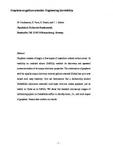
experimentally measured transmission spectra of the single-layer graphene (SLG) metamaterial (with hexagonal meta-atoms) clearly show the gate voltage dependent resonant features (Fig. 2a): (1) the resonant frequency (f0) is red-shifted with increasing |ΔV|, where |ΔV| = |VCNP –Vg| and VCNP is the charge neutral gate voltage. This red-shift is mainly due to the increase in the sheet conductivity of graphene; (2) the width of resonance is broadened with increasing |ΔV|, which is caused by additional Joule losses from the metallic graphene layer; (3) the on-resonance transmission, T(f0), increases in proportion to |ΔV|1/2 in the SLG metamaterial as a result of weaker terahertz wave coupling to the resonance of meta-atoms with increasing conductivity in the graphene layer (Fig. 2g); and (4) the off-resonance transmission is supressed with increasing |ΔV| due to the gate-induced broadband electro-absorption in the graphene layer. The VCNP of the device under test is estimated to be ~350 V from the measured trace of transmission minima (dashed line in Fig. 2a). In order to quantify the active tuning capability more clearly, relative changes in transmission, -ΔT/TCNP (where ΔT=T-TCNP), are plotted as a function of Vg, as shown in Fig. 2b. At the maximum ΔV = 850 V, the measured ΔT/TCNP reaches approximately -90 % when the frequency approaches f0 in SLG metamaterial. In the case of a multilayer graphene (MLG) metamaterial, the measured ΔT/TCNP exceeds -140 % with a relatively small ΔV = 120 V (see Supplementary Information for the MLG metamaterials). It is noteworthy that this huge modulation is realized solely by the inclusion of a graphene layer of infinitesimal thickness (< λ/1,000,000 for SLG) into the metamaterial of deep subwavelength-scale thickness (~λ/100). The relative change in transmission per unit thickness was measured to be 6
34 %/μm, which exceeds that of all previously reported 2DEG-based terahertz modulators. Moreover, a large degree of broadband modulation (more than 10 %/μm) at the off-resonance frequencies (0.1–0.6 and 1.2–2.5 THz) is possible. Figure 2c shows the measured phase change Δ in SLG metamaterials as a function of Vg. The maximum value of Δ exceeds 40 degrees at 0.65 THz (Δ ~ 70 degrees for the MLG graphene metamaterial, see Supplementary Information). This substantial gate-controlled phase modulation of terahertz waves can be further increased by reducing the gap between the hexagonal meta-atoms and/or by stacking multiple layers of deep subwavelength-scale graphene metamaterial13. For a quantitative comparison with experimentally observed phenomena, the transmission spectra of active graphene metamaterials were calculated by a finite element analysis. In order to model the atomically thin graphene layer in electromagnetic wave simulations, the complex conductivity of graphene estimated via Kubo’s formula was converted to a dielectric constant for a very thin effective layer7. The conductivity of graphene (σg = σinter + σintra) at terahertz frequencies is dominated by the contribution from the intraband transition and can be cast in a Drude-like form. The applied gate voltage leads to a carrier density change and consequently shifts the Fermi level (EF) according to the following formula (for SLG): EF = sign(ΔV)ħvF(απ|ΔV|)1/2, where vF ≈ 1 × 10⁶ ms-1 is the Fermi velocity and α ≈ 5.12 × 109 cm-2V-1 is the EOT gate capacitance in the electron charge, respectively. Inserting these values into Kubo’s formula, the transmission (Fig. 2d), the relative change in transmission (Fig. 2e), and phase change (Fig. 2f) were calculated as a function of gate voltage changes. All of the gate voltage dependent 7
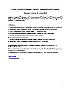
resonant features were excellently reproduced in the simulations with a single fitting parameter for scattering time τ = 15 fs, as shown in Fig. 2g. The fitted scattering time is comparable to that previously reported for thermally grown graphene28. It is worth noting that the nonlinear relative change in transmission can hardly be fitted with the multilayer approximation29, which provides additional evidence on the embedded singlelayer graphene (single-layer graphene characterization is given in the Supplementary Information). Detailed dynamics of charge carrier transport can be clearly visualized with the numerical simulation. At CNP, the conductivity of the graphene layer is still small enough so as not to perturb the LC resonance of hexagonal meta-atoms. With increasing |ΔV|, the graphene becomes more conductive such that fewer charge carriers accumulate at the edge of the meta-atoms as charge carriers can leak into adjacent metaatoms through conductive graphene channels, as shown in the field simulation depicted in Fig. 2h, i. To investigate gate-controlled behaviours in an artificial multi-resonance system hybridized with single-layer graphene, asymmetric double split rings (aDSR)30 are utilized as a unit cell of meta-atoms. Figure 3 shows the gate-dependent transmission for aDSR graphene metamaterial. With broken symmetry in aDSR meta-atoms (asymmetric factors of θ1 = 15 ° and θ2 = 10 ° are defined in Fig. 3e), a sharp Fano-like resonance (‘trapped mode’, marked as I in Fig. 3c) is observed in the low-frequency side of the fundamental electric ‘dipole mode’ resonance (marked as II in Fig. 3c). The simulated current densities for these two distinct modes in aDSR are depicted by the arrows in the left panel inside Figs. 3e, f. Compared to the electric dipole mode (in-phase current 8
oscillation), the trapped mode resonance (out-of-phase current oscillation) exhibits a higher quality factor due to weak free-space coupling and low radiation losses. At the trapped mode resonance, the absorption of the metamaterial reaches a maximum value of 40 %, the main contribution arising from substrate and metallic losses (the intrinsic terahertz absorption in the graphene layer is substantially lower at CNP10). As we increased the gate voltages, absorption increased substantially, except in the vicinity of the Fano-like resonance, by carrier-induced electro-absorption in the single-layer graphene (lower panel of Fig. 3c). Hence, the gate-dependent transmission changes showed different behaviours for these two modes, as exhibited in Fig. 3d. The onresonance transmission of the trapped mode showed little change (-ΔT/TCNP < 5 %) with gate voltages, whereas for the electric dipole mode, the changes are substantial, amounting to about 40 %. Such broadband tunable absorption means that the graphene metamaterial could be used as a platform to attain a perfect absorber by patterning and/or stacking graphene layers. In addition to promising amplitude and phase modulation predictable on the basis of the carrier dynamics of ideal graphene, active graphene metamaterial exhibits a considerable amount of gate-controlled optical hysteresis. The controllable hysteretic behaviours in the realistic graphene on a substrate21-24, when combined with the metamaterial, can alternatively be utilized as a route toward the development of an electrically controllable photonic memory. The photonic memory effect in our device can be mainly attributed to charge trapping phenomena at the grain boundaries or defect sites in a large-area CVD-grown graphene layer as well as adsorption of H2O molecules 9
on the polyimide substrate.
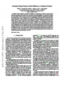
Figure 4a shows such hysteretic behaviour in the
transmission at a fixed frequency for a cyclic change of the gate voltage (for active graphene metamaterial with hexagonal meta-atoms). For this measurement, the gate voltage was swept at a rate of 50 V/min. Figure 4b shows a flip-flop operation in transmission (top panel) and a time-trace of measured resonant frequency (middle panel). Here, the ‘write (set)’ and ‘erase (reset)’ inputs were implemented by applying a short pulse signal of the gate voltage (pulse width = 1 second, lower panel). The peak gate voltage of pulses was set to -300 V (write) and 300 V (erase), respectively. The state of the transmission and/or resonant frequency of the SLG metamaterial was read at zero gate voltage (Vg = 0 V, dashed line in Fig. 4a). It is worthwhile to note that the measured retention time of the active graphene metamaterial was proportional to both the magnitude and the pulse width of the applied gate voltage (see Supplementary Information for the results in MLG metamaterial, for which the retention time is larger). With the given gate voltage pulses (±300 V for 1 sec), the retention time is estimated to be around 20 min, which is comparable to the value of CVD-grown SLG ferroelectric memory24 (Fig. 4b). For longer memory retention times, oxidative graphene would be superior to an intrinsic graphene layer due to oxygen-related, stable memristive phenomena21,22. In conclusion, we experimentally demonstrated an electrically controllable lightmatter interaction in a gate-controlled active graphene metamaterial.
The exotic
electrical and optical properties of graphene, when enhanced by the strong resonance of meta-atoms, lead to a very strong light-matter interaction in a manner that allows 10
persistent switching and linear modulation of low energy photons in the extreme subwavelength-scale (~λ/1,000,000).
Surprisingly, low energy photons were fully
controlled while being transmitted through gate-controlled, one-atom-thick, single-layer graphene integrated with strongly coupled meta-atoms. By stacking the deep subwavelength-scale planar graphene metamaterial, further enhancement of the lightmatter interaction is expected. Benefitting from the controllable light-matter interaction, the gate-controlled active graphene metamaterials are expected to provide a myriad of important applications, particularly in the dynamic control of terahertz waves, tunable transformation-optics devices, and photonic memory devices.
11
Method Summary Fabrication processes for the gate-controlled active graphene metamaterial All metallic parts of the graphene metamaterial were made of 100-nm-thick gold with a 10nm-thick chromium adhesion layer. Graphene was grown by CVD in order to cover the entire area of the metamaterial (15 × 15 mm2). A bare silicon wafer was used as a sacrificial substrate. In order to construct the active graphene metamaterial on the sacrificial substrate, a polyimide solution (PI-2610, HD MicroSystems) was spin-coated and fully cured using a two-step baking process, resulting in a final polyimide thickness of 1 μm. In order to define the bottom EOT electrode on the prepared polyimide layer, UV photolithography and electron-beam evaporation were followed by a metal lift-off technique. Repeating the same polyimide stacking processes as employed for the first layer, the metallic meta-atoms are then insulated from the bottom electrode. The metallic meta-atoms were patterned using the same processes as for the bottom electrode. Then, the graphene (SLG on Cu foil, MLG on Ni/SiO2/Si substrate) was transferred and conformally attached to the array of meta-atoms. After the graphene layer had been transferred onto the meta-atoms, a ground electrode was defined on the graphene layer using a shadow mask. For the symmetry of graphene metamaterials in the direction of the terahertz wave propagation, a polyimide layer and a top EOT electrode (optional) were stacked. After opening the electrical contact via O2 plasma etching, the freestanding and flexible active graphene metamaterials were peeled off of the silicon substrate. Finally, the active graphene metamaterials were soldered to a drilled PCB substrate.
12
References 1 2 3 4 5 6 7 8 9 10 11 12 13 14 15 16 17 18 19
Geim, A. K. & Novoselov, K. S. The rise of graphene. Nat Mater 6, 183-191 (2007). Wang, F. et al. Gate-variable optical transitions in graphene. Science 320, 206209 (2008). Bonaccorso, F., Sun, Z., Hasan, T. & Ferrari, A. C. Graphene photonics and optoelectronics. Nat Photonics 4, 611-622 (2010). Ju, L. et al. Graphene plasmonics for tunable terahertz metamaterials. Nat Nanotechnol 6, 630-634 (2011). Koppens, F. H. L., Chang, D. E. & de Abajo, F. J. G. Graphene Plasmonics: A Platform for Strong Light-Matter Interactions. Nano Lett 11, 3370-3377 (2011). Liu, M. et al. A graphene-based broadband optical modulator. Nature 474, 64-67 (2011). Vakil, A. & Engheta, N. Transformation Optics Using Graphene. Science 332, 1291-1294 (2011). Echtermeyer, T. J. et al. Strong plasmonic enhancement of photovoltage in graphene. Nat Commun 2, 458 (2011). Papasimakis, N. et al. Graphene in a photonic metamaterial. Opt. Express 18, 8353-8359 (2010). Maeng, I. et al. Gate-Controlled Nonlinear Conductivity of Dirac Fermion in Graphene Field-Effect Transistors Measured by Terahertz Time-Domain Spectroscopy. Nano Lett 12, 551-555 (2012). Pendry, J. B., Holden, A. J., Robbins, D. J. & Stewart, W. J. Magnetism from conductors and enhanced nonlinear phenomena. IEEE Transactions on Microwave Theory and Techniques 47, 2075-2084 (1999). Smith, D. R., Padilla, W. J., Vier, D. C., Nemat-Nasser, S. C. & Schultz, S. Composite Medium with Simultaneously Negative Permeability and Permittivity. Phys Rev Lett 84, 4184-4187 (2000). Choi, M. et al. A terahertz metamaterial with unnaturally high refractive index. Nature 470, 369-373 (2011). Ferguson, B. & Zhang, X.-C. Materials for terahertz science and technology. Nat Mater 1, 26-33 (2002). Hu, T., Padilla, W. J., Xin, Z. & Averitt, R. D. Recent Progress in Electromagnetic Metamaterial Devices for Terahertz Applications. IEEE Journal of Selected Topics in Quantum Electronics 17, 92-101 (2011). Kleine-Ostmann, T., Dawson, P., Pierz, K., Hein, G. & Koch, M. Roomtemperature operation of an electrically driven terahertz modulator. Appl Phys Lett 84, 3555-3557 (2004). Sensale-Rodriguez, B. et al. Unique prospects for graphene-based terahertz modulators. Appl Phys Lett 99, 113104 (2011). Chen, H. T. et al. Active terahertz metamaterial devices. Nature 444, 597-600 (2006). Chen, H.-T. et al. A metamaterial solid-state terahertz phase modulator. Nat Photon 3, 148-151 (2009). 13
20 21 22 23 24 25 26 27 28 29 30
Shrekenhamer, D. et al. High speed terahertz modulation from metamaterials with embedded high electron mobility transistors. Opt Express 19, 9968-9975 (2011). Wang, H. M., Wu, Y. H., Cong, C. X., Shang, J. Z. & Yu, T. Hysteresis of Electronic Transport in Graphene Transistors. Acs Nano 4, 7221-7228 (2010). Echtermeyer, T. J. et al. Nonvolatile Switching in Graphene Field-Effect Devices. IEEE Electron Device Letters 29, 952-954 (2008). Jeong, H. Y. et al. Graphene Oxide Thin Films for Flexible Nonvolatile Memory Applications. Nano Lett 10, 4381-4386 (2010). Song, E. B. et al. Robust bi-stable memory operation in single-layer graphene ferroelectric memory. Appl Phys Lett 99, 042109-042103 (2011). Driscoll, T. et al. Memory Metamaterials. Science 325, 1518-1521 (2009). Kim, K. S. et al. Large-scale pattern growth of graphene films for stretchable transparent electrodes. Nature 457, 706-710 (2009). Martín-Moreno, L. et al. Theory of Extraordinary Optical Transmission through Subwavelength Hole Arrays. Phys Rev Lett 86, 1114-1117 (2001). Dawlaty, J. M. et al. Measurement of the optical absorption spectra of epitaxial graphene from terahertz to visible. Appl Phys Lett 93, 131905-131903 (2008). Yu, Y.-J. et al. Tuning the Graphene Work Function by Electric Field Effect. Nano Lett 9, 3430-3434 (2009). Fedotov, V. A., Rose, M., Prosvirnin, S. L., Papasimakis, N. & Zheludev, N. I. Sharp Trapped-Mode Resonances in Planar Metamaterials with a Broken Structural Symmetry. Phys Rev Lett 99, 147401 (2007).
We thank B. H. Hong for the discussion on the application of graphene, Y.-J. Yu for the discussion on carrier transport in graphene, J. H. Han for the characterization of graphene, and H. Choi for proofreading the manuscript. This work was supported by the National Research Foundation of Korea (NRF) grant funded by the Korea government (MEST) (No. 2008-0062235, 2009-0069459, 2010-0012058, 2011-0020186, and 2011-0028151). S. S. L acknowledges the support by the NRF of Korea grant funded by the MEST (No. 2010-0027050). S.-Y. C acknowledges the GFR Program (2011-0031640) sponsored by the MEST. C.-G. C acknowledges the Nano R&D Program (2011-0019169) through the NRF of Korea funded by the MEST and the Creative Research Program of the ETRI (11YF1110). X. Z acknowledges the support from US NSF Nano-scale Science and Engineering Center (NSEC) for Scalable and Integrated Nanomanufacturing (SINAM) at UC Berkeley (Grant No.CMMI-0751621) Correspondence and requests for materials should be addressed to B. M. (
[email protected]). 14
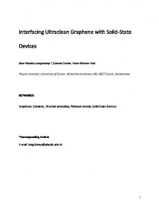
Figure 1 Schematic view and device images of gate-controlled active graphene metamaterials. a, Schematic rendering of a gate-controlled active graphene metamaterial composed of a single atomic layer of graphene deposited on a layer of hexagonal metallic meta-atoms (a unit cell of L = 60 μm, g = 5 μm, and total device thickness d = 4.2 μm) and top/bottom extraordinary transmission (EOT) electrodes (periodicity = 6 μm, metal width = 4 μm) embedded in a dielectric material of 4.22 μm thickness. The polarization of the incident THz wave is perpendicular to the line electrode, as indicated by the arrows. b, Optical micrograph of the fabricated gate-controlled active graphene metamaterial without the top electrode giving a clear view of the hexagonal meta-atoms. c, Fully integrated gate-controlled active graphene metamaterial attached to a drilled printed circuit board (PCB) for THz-TDS measurement (B: connected to bottom EOT electrode, G: connected to graphene layer). Inset: Magnified view of the gate-controlled active graphene metamaterial. d, Optical image of the fabricated large-area metamaterial wound around a glass rod, showing its high degree of flexibility. Figure 2. Gate-controlled amplitude and phase changes of terahertz waves transmitted through the hexagonal graphene metamaterials
Measured
spectra of a, transmission (T), b, relative change in transmission (-∆T/TCNP), c, phase change (∆ϕ) plotted as a function of gate voltages. d, e, f, Simulated results with a single layer graphene (SLG) approximation are plotted, corresponding to a, b, and c, respectively. A fitting parameter for scattering time
is set to 15 fs. g, The relative change in transmission at a resonance frequency of 0.86 THz is plotted. Scatters and lines are for the experimental and simulation data, respectively. The measured nonlinear trend in transmission change is 15
excellently fitted by the SLG approximation. h, Saturated electric field (at 0.86 THz) within a unit cell for the graphene metamaterial with (lower panel) and without applying gate voltage (upper panel). i, Current density (at 0.86 THz) in the meta-atom (left panel) and the graphene layer (right panel) with increasing gate voltages. Figure 3. Gate-controlled amplitude change of terahertz waves transmitted through the asymmetric double split ring (aDSR) graphene metamaterials a, Measured relative change in transmission of the aDSR graphene metamaterials is plotted as a function of gate voltage. b, Simulated results obtained with the SLG approximation show good agreement with experimental observation.
c,
Two distinct resonances are marked I (trapped mode) and II (dipole mode) with different tuning behaviours. As the gate voltage increased, transmission at the dipole mode resonance is significantly increased; however, the trapped mode transmission showed little change, where the origin is from a small change in the absorption for the trapped mode (lower panel).
d, Relative changes in
transmission for the two modes are plotted along with the simulations. e, Gatedependent current density for the trapped mode is shown with the arrows in a unit cell of aDSR meta-atom (left panel) and graphene layer (right panel). f, Corresponding current density for the dipole mode. Figure 4. Electrically-controlled photonic memory operation with the gatecontrolled active graphene metamaterials
a, Hysteresis behaviour of on-
resonance transmission for a cyclic change of the gate voltage (with a sweeping rate of 50 V/min). b, Binary memory operation in the transmission (top panel), a measured time-trace of resonant frequency (middle panel), and gating pulse 16
signal (pulse width = 1 sec, lower panel). The observed memory retention time is estimated to be around 20 min.
17
Lee, Figure 1
18
Lee, Figure 2
19
Lee, Figure 3
20
Lee, Figure 4
21
Supplementary Information for “Switching terahertz waves with gate-controlled active graphene metamaterials” Seung Hoon Lee, Muhan Choi, Teun-Teun Kim, Seungwoo Lee, Ming Liu, Xiaobo Yin, Hong Kyw Choi, Seung S. Lee, Choon-Gi Choi, Sung-Yool Choi, Xiang Zhang & Bumki Min
Here, we present the preparation and characterization of graphene, the design of extraordinary optical transmission (EOT) gate electrodes, the experimental/numerical data on active multilayer graphene (MLG) metamaterials, and the results of control experiments on samples without graphene.
I.
Preparation and characterization of graphene A.
CVD growth of SLG and MLG and their transfer method
B.
Characterization of CVD-grown graphene
II.
Design of EOT gate electrodes
III.
Terahertz wave transmission properties of active MLG metamaterials
IV.
A.
Amplitude modulation
B.
Phase modulation
C.
Hysteretic behaviours
Measurement of control samples without graphene layer
1
Figu ure S1 | Sc chematics of o the gate e-controlled d active graphene me etamaterialls and their optical images a, Schemattic view on n fabricatio on of the active graphene meta amaterial (P PI: polyimid de, td: total device thicckness). b, Optical miicrographs of the fabricated hexa agonal meta a-atoms c, A Asymmetricc double split ring meta-atoms.
2
I.
Preparation and characterization of graphene A. CVD growth of SLG and MLG and their transfer method
For the fabrication of samples, we used commercially available single-layer graphene (SLG) from Graphene Square Inc., and multilayer graphene (MLG) grown by in-house thermal chemical vapour deposition (CVD). For MLG growth, 300-nm-thick nickel was deposited as a catalyst layer on a SiO2/Si substrate by an electron-beam evaporator. Prepared Ni/SiO2/Si substrate was loaded in a quartz tube furnace, then heated up to 1,000 °C under vacuum condition (30 mTorr) with a constant H2 flow (10 sccm). MLG was grown by flowing gas mixtures (CH4:H2 / 30:10 sccm) for 3 min and MLG on the substrate was dismounted from the furnace and cooled down to room temperature (25 °C) at a cooling rate of 5 °C/min under Ar gas flow of 1,000 sccm. In order to transfer the CVD-grown SLG and MLG to a polyimide substrate, a polydimethylsiloxane (PDMS) film was used to minimize undesired cracks and solventinduced effects. The thermally grown SLG (MLG) on the Cu foil (Ni/SiO2/Si substrate) was peeled off from the substrate after 8-hour etching in a 0.1 mol% ammonium persulfate (3-hour etching in a 12.5 mol% iron chloride) solution. After a two-step rinsing process with DI water, the graphene layer was successfully transferred and conformally attached to the prepared polyimide layer, on which the meta-atoms were patterned.
B. Characterization of CVD-grown graphene Raman spectroscopy was used with a 532 nm excitation laser for the characterization of graphene layers. The SLG and MLG, grown in the same batch for samples used in the main manuscript, were transferred onto a 300-nm-thick SiO2 substrate. Based on 2D/G intensity ratios and the full width at half maximum (FWHM), the number of graphene layers was estimated. As shown in Fig. S2a, the location and FWHM of 2D peak is 2,686 cm-1 and 30 cm-1, respectively. For MLG (Figs. S2b-d), the number of layer varies spatially
3
med by transsmission ellectron and is estimateed to be appproximatelyy 1 to 10, as confirm TEM). A crross-sectionaal TEM imaage of the fa fabricated MLG M metam material micrrographs (T show ws that therre are severaal discontinuuities with defects d sitess, such as gaps g and wriinkles, whicch can be attributed tto the one of the dom minant causses of electtrically conttrolled phottonic memoory effects.
Figu ure S2 | Ch haracterizattion of CVD D-grown grraphene by y Raman sp pectroscop py and tran nsmission e electron microscopy (TEM). a, Raman R specctrum of SL LG shows th hat the 2D p peak is loca ated at 2,686 cm-1 and the full widtth at half ma aximum (FW WHM) is about 30 cm-11. b, Rama an spectrum m of MLG sh hows that th he FWMH o of 2D peak is larger th han 45 cm-11. c, A cross-sectiona al TEM imag ge of the a active MLG metamateriial. Betwee en the polyyimide layer and meta allic meta-a atoms, laye ered graphe ene is clea arly identifie ed. d, Average intensity profile accross the grraphene layyer marked b by red arrow ws.
4
e electrode es II. Design off EOT gate material was designed too apply a unniform The gate electroode for the active graphhene metam w maintaaining a larrge transmisssion of terrahertz electric field inn the grapheene layer while ment, an arraay of deep ssubwavelenngth-scale m metallic wavves. In orderr to satisfy thhis requirem wirees, referred to as an EO OT electrodee, was optim mized. Figuure S3a show ws the schem matics (inseet) of the EOT electrrode dimennsion with numericallyy calculatedd transmission at terahhertz frequeencies (0 - 2 THz). T The EOT eleectrodes forr the sample were fabrricated withh the perioddicity (a) off 6 μm and the gap widdth (a - w) of 2 μm. A Although thhe gap widtth of the w wire array iis in the ddeep subwavvelength-sccale (~λ/1500 at 1 THzz), the simuulated transmission is ffound to be over 89 peer cent in the frequencyy band of innterest. Thiss large trannsmission can be explained on thhe basis off well-know wn phenomeena of extraaordinary optical o transmission1.
Figure S33b shows thhe calculateed and meaasured
transmission thrrough the acctive grapheene metamaaterial with E EOT electroodes.
Figu ure S3 | EO OT electrod des for the gate-contrrolled active graphene e metamate erials. a, S Schematic re endering of EOT electrrodes along with simula ated transm mission specctra for wire e widths of 3 3, 4, and 5 m. b, Pola arization dep pendent transmission tthrough the active grap phene metamaterials in ntegrated wiith EOT elecctrodes.
5
nsmission n propertie es of activ ve MLG me etamateria als III. Terahertzz wave tran A A. Amplitu ude modu ulation
Figu ure S4 | Amplitude A modulation n of terahe ertz waves s with the gate-conttrolled activ ve MLG m metamateria al. a, Meassured transm mission spe ectra as a ffunction of ∆V ∆ (=
VCNP –Vg) from m 0 to 120 V V. With inccreasing ga ate voltage, the resonant frequenccy was red--shifted and d broadened d by Joule losses in th he graphene layer. Relative chan nge in transmisstion, --∆T/TCNP exceeded -140 % at 12 20 V. b, Fo or compariso on, the simulated transmission off the active graphene m metamateria als are plotte ed as a funcction of the Fermi leve el in a graph hene layer (H Here, we asssumed the intraband sscattering tim me of 25 fs)).
6
B B. Phase modulatio m n
Figu ure S5 | Ph hase modu ulation of terahertz w waves with h the gate--controlled d MLG mettamaterials.
a, Meassured phasse change of teraherttz waves th hrough the MLG
meta amaterials as a functio on of ∆V. Maximum p phase chan nge exceeded /3 radia ans at
∆V = 120 V. The effectiive refractivve indices were estim mated from the S-para ameter extra action meth hod and we ere shown iin the lower panels. T The gate-controlled refrractive inde ex was varie ed from 4 to 9 with in ncreasing g gate voltage e at resonant frequenccy. b, Simulated phasse change of o terahertzz waves thro ough the acctive graphe ene metam material of Fermi energy levell. c, Simula ated wavefrronts of terrahertz wavve are as a function o show wn as a fun nction of Ferrmi level at a frequencyy of 0.64 TH Hz. Phase d delays are clearly c obse erved with increases in n the Fermi level. l
7
C C. Hystere etic behaviours
Figu ure S6 | Ga ate-depende ent optical hysteresis s of MLG m metamateria als. a, Hystteresis curvve of the ga ate-controlle ed active graphene metamaterial (VCNP ≈ 20 0 V, gate vvoltage swe eeping rate o of ~3 V/min, transmissiion changess following tthe path ind dicated by arrows). gate voltage e sweeping rate and memory The hysteresis curve was dependent upon the g retention time.
b, For ssmall gate voltage ch hange nearr CNP (from m -50 to 5 50 V),
m att 1 THz was varied lin nearly with llittle hystere esis. c, Forr large transmission measured e voltage ch hange betwe een -80 to 8 80 V, a hyste eretic behavviour was cllearly obserrved. gate
8
Figu ure S7 | Measured M rretention time t of the e MLG me etamaterials.
a, Mea asured
retention time a as a function n of gate vo oltage. An in nitial on-resonance tran nsmission (0 0.148) plying gate voltage to 0.307 at 15 50 V. Afterr 1 min dop ping at at 0 V is shifted when app ous gate vo oltages, the transmissio on was reco overed to the initial valu ues. Within n small vario gate e voltage a at 30 V, the resonancce recoveryy time wass fast enough as not to be mea asured using g our THz-T TDS setup. b, Doping time depen ndent recove ery time at a gate volta age of 80 V V. As the ele ectro-static d doping time (gating time) is increased, the rettention time e also increa ased.
9
ment of co ontrol sam mples witho out graphe ene layer IV. Measurem In order to cconfirm the effect oof gate-conntrolled graaphene in active graaphene ( um and 8 um) metaamaterials, two grapheene-free meetamaterials with differrent gaps (5 weree fabricatedd and their transmissioon spectra were w measuured with a variation inn gate voltaages. As caan be seen ffrom Fig. S S8, the meaasured transm mission speectra were aalmost invaariant to the change in gate g voltagee applied to tthe top and bottom EOT T electrodess.
Figu ure S8 | Me easured tra ansmission spectra off the metam materials w without grap phene laye er. The gate e voltage wa as varied fro om 0 to 100V V.
Refeerences 1
mi, H. F., Thio, T. & Wolff, P. A. Ebbesenn, T. W., Lezec, H. J., Ghaem Extraorddinary opticcal transmisssion througgh sub-wavvelength hoole arrays. N Nature 391, 6677-669 (19988).
10