System Design and Verification Process for LHC Programmable Trigger Electronics1 Dario B. Crosetto 900 Hideaway Pl, DeSoto, Texas 75115
[email protected],
[email protected]
Abstract The rapid evolution of electronics has made it essential to design systems in a technology-independent form that will permit their realization in any future technology. This article describes two practical projects that have been developed for fast, programmable, scalable, modular electronics for the firstlevel trigger of Large Hadron Collider (LHC) experiments at CERN, Geneva. In both projects, one for the front-end electronics and the second for executing first-level trigger algorithms, the whole system requirements were constrained to two types of replicated components. The overall problem is described, the 3D-Flow design is introduced as a novel solution, and current solutions to the problem are described and compared with the 3D-Flow solution. The design/verification methodology proposed allows the user's real-time system algorithm to be verified down to the gatelevel simulation on a technology-independent platform, thus yielding the design for a system that can be implemented with any technology at any time.
the related software and hardware of the 3D-Flow system which together make possible a simplified hardware implementation providing higher performance at lower cost. The pipelining technique has been used for many years in computer CPUs, and has subsequently been used also by the designers of first-level triggers for High Energy Physics (HEP).
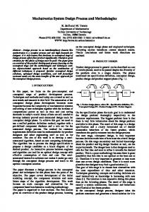
A. Current pipelined systems in microprocessors and HEP Pipelining is an implementation technique used to speed up CPUs or trigger systems in HEP, in which multiple instructions (or operations) are overlapped in execution. An instruction of a CPU (or trigger electronics in HEP) can be divided into small steps, each one taking a fraction of the time to complete the entire instruction. Each of these steps is called a pipe stage or pipe segment (see Fig. 1, where St_1 = Stage 1). The stages are connected to one another to form a pipe. PIPELINE in Microprocessors
I. INTRODUCTION This article addresses the issues reported in Table 1. Only a full understanding of the interrelationships between all the issues – the requirements of the application, commonality of function, flexibility, modularity, scalability, and familiarity with current hardware and software – can lead to the best design. To demonstrate that the 3D-Flow [1] system represents the optimum design, some results of an example of a specific application that show its advantages compared to the current approaches are described. These examples include the simplified backplane and simplified electronics based on a single type of board. An in-depth analysis of the requirements has been made, and a conceptual abstraction is presented contrasting the 3DFlow solution with the solution used in current applications. First, the pipeline concept as it is currently used in microprocessors and trigger systems in HEP is described. Second, the modified feature of extending the execution time in one pipeline stage is presented. Third, the different solutions using the old scheme and the novel 3D-Flow approach are compared, and the advantages and benefits of the proposed solution are pointed out.
II. THE KEY CONCEPT The key concept is a switching element intrinsic in each 3D-Flow processor that allows for a processing time in a pipelined stage that is longer than the time interval between two consecutive input data. Other parts of the key elements are
CPU
Memory Write Fetch Decode Execute Access back 25ns
25ns
25ns
25ns
25ns
f=40 MHz St_1 T=25ns
St_2
St_3
St_4
St_5
Execute Level-1 Trigger PIPELINE in High Energy Physics
Trigger electronics
ADC
FrontEnd
Figure 1. Pipelining implementation technique in current CPUs or HEP fast electronics
The instruction (or datum in HEP) enters one end and exits from the other. At each step, all stages execute their fraction of the task, passing on the result to the next stage and receiving from the previous stage simultaneously. The example described in this article refers to a speed of 40 MHz, but is not limited to that speed. Rather, the described approach applies to any speed which can be achieved with any technology. Stage 1 either receives a new datum from the sensors every 25ns and converts it from analog to digital in HEP, or fetches a new instruction in a CPU. The complete task (instruction in a CPU) is executed in the example of Figure 1 in 5 steps of 25ns each. In such a pipelined scheme, each stage has an allocated execution time that cannot exceed the time interval between two consecutive input data (or instruction in a CPU).
1 This material is based upon work partially funded by the Department of Energy under Grant No. DE-FG03-95ER81905.
B. Extending the execution time in one pipelined stage
C. The intrinsic bypass switch in each 3D-Flow processor
The first-level trigger algorithm in HEP experiments requires the performance of a sophisticated analysis on the input data to optimally identify the particles.
Input data and output results flow from the “Top layer” to the “Bottom layer” of a stack of the 3D-Flow system as shown in Figure 3 and references [1] and [3].
The designers of electronics for the first-level trigger in HEP have attempted to achieve the above goal by using cable logic circuits, fast GaAs technology, and fast memories. All these solutions have assumed that the processing time in one pipelined stage may not exceed the time interval between two consecutive input data.
The system is synchronous. The first layer has only input data at the top port which are received from the sensors, while the bottom layer has only results at the output port.
In the above application as well as in others, however, it is desirable to extend the processing time in a pipeline stage. The 3D-Flow system [2] introduces a layered structure of processors and an intrinsic bypass switch in each processor that can extend this processing time in one pipelined stage. Each 3D-Flow processor in “Stage 3” (St_3 in Fig. 2) executes the complete task of the first-level trigger algorithm just as a computer in a large computer farm reconstructs a complete event. There is no division of the trigger algorithm into small steps, each executed by a different processor (or circuit) as would have been the case in a normal pipelined system. If, for example, the time to execute the algorithm is ten times the time interval between two consecutive data, the processor of the first layer fetches one set of data from the top port connected to the sensors and (without processing them) moves the following nine sets of data to the subsequent layers via a bypass switch intrinsic to each 3D-Flow processor [1]. The processor in the second layer will fetch one datum, move one result received from layer one and move eight input data received through layer one to the following layers through the internal bypass switches, and so on. Thus, the key element of the 3D-Flow system to extend the processing time beyond the time interval between two consecutive input data, is the intrinsic bypass switch on each processor which allows a longer processing time proportional to the number of layers. 25ns
f=40 MHz T=25ns
St_1
25ns
St_2
>25ns
St_3
25ns
St_4
25ns
St_5
25-250 ns 1-10 layers of 3D-Flow Figure 2. One pipeline stage needs to have the processing time extended. The electronics of Stage 3 (St_3) consists of several layers of 3D-Flow processors called a “stack.” Each 3D-Flow processor executes the entire first-level trigger algorithm, similar to a computer in a farm that is reconstructing an event. Programmability has been achieved, and ultra-fast cable logic implementation is not necessary. An intrinsic bypass switch in each 3D-Flow of the stack performs the function of routing the incoming data to the first idle processor.
In the example of a 3D-Flow system shown in Figure 3, every eight clock cycles a new set of data (identified in Figure 3 as i1, i1; i2, i2, i3, i3, etc.) is received by Layer 1 of the 3DFlow processor stack. In the same example, each processor requires 24 cycles to execute the indivisible algorithm. The column of the table of Figure 3 labeled “switch status #34, #35” shows the position of the switches of the processors in Layer 1, Layer 2, and Layer 3 respectively. The processors in Layer 2 have the internal switches in the open position allowing input/output to the processor. This is called position ‘i’. The internal switches in Layer 1 and 3 processors are in the closed position, blocking entry to the processor and moving data from the top port of the processor to the bottom port through the bypass switch without processing them. This position of the switches is called position ‘b’. In the example, the first set of data (i1, i1) is fetched from the processors in the first layer via the internal switches set in position ‘i’. Upon entry of the data into the processor, the internal switches are set in position ‘b’. The second set of data received at Layer 1 at the clock cycle 9 and 10 are moved via the internal switches in position ‘b’ to the processors at Layer 2 which are in position ‘i’ and free to start the execution of the algorithm. The data received at cycle 17 and 18 are moved to Layer 3 via the internal switches in position ‘b’ of Layer 1 and Layer 2, these layers being occupied in processing the previous data. When the internal switches of the processors at Layer 1 are set in position ‘i’ at the clock cycles 25 and 26 as the new set of data are fetched by the processors at this layer, the results of the processing on the previous set of data on the same layer are sent to Layer 2 to be moved to the last layer of the 3D-Flow system. At each clock cycle the data not processed by the processor, but only moved from the top port to the bottom port through the bypass switches are also buffered into a register as shown in Figure 3. Thus for each clock cycle a datum advances into the “flow” from the first layer of processors to the last layer, one layer at a time. This technique simplifies the hardware construction in allowing implementation of a 3DFlow system made of a variable number of layers. The hardware simplification results from data at the bottom port being registered and the propagation delay of the signals (traces, register setup time, etc.) only needing to be satisfied between two adjacent layers. This is independent of the total number of layers of the system. The table to the left of Figure 3 shows how the processors at each layer count the input data, results, bypass data, and bypass results.
Figure 3. The flow of the input data and output results in a 3D-Flow system. The example shows a 3D-Flow system executing an algorithm that requires three times the time interval between two consecutive input data where the input data rate is 1/8 the processor clock frequency. The left column of the table at the left shows how processors at each layer count the input data, bypass data, results, and bypass results in order to set the bypass switches appropriately at the processors at each layer. An example of the position of the bypass switches for clocks #34 and #35 is shown in the other columns of the table.
D. Advantages and benefits of the 3D-Flow solution compared to existing designs Figure 4 compares the different solutions in extending the processing time in a pipeline stage. For a single channel, the current approach could provide a solution, however inefficient and costly; however, for multiple channel systems requiring data exchange between neighboring PEs, (see Fig. 4f) the current approach does not offer a practicable solution capable of implementation. Figure 4a shows the problem that needs to be solved. The processing time in a pipeline stage must be extended, because the operations in that particular stage are indivisible. Examples of tasks that are indivisible are: a) the processor is awaiting data from several neighbors which cannot be received within 25ns; b) some “branch” instructions in the program take longer than 25ns; or c) the algorithm is indivisible because the intermediate results generated would be too large to be transmitted from one stage to the next and because the algorithm is too complex to be executed in 25ns. In case the problem can be solved with twice the processing time, a solution currently implemented in some applications is to replicate the circuit as shown in figure 4b and to add a switch at the input of the two identical circuits and one at the output. While the switch is routing one datum to one circuit, the other circuit can process for a longer time. At the arrival of the next datum after 25ns, the switch will route it to the second circuit, allowing the first one to spend 50ns on processing it, and so on. The switch at the output will collect the results from the two circuits alternatively every 25ns. If more processing time is required, another identical circuit is added to increase it to 75ns, and the general switches connected at the input and output of the three identical circuits also need to be changed (see Figure 4c). This scheme is costly and impractical from a construction standpoint, because when an identical circuit is added in parallel the entire design must be changed. Traces connecting the different circuits on a printed circuit board (PCB) change in length, and the
difference between short and long traces increases as they need to reach more components. Electrical conditions on the PCB change and become more complex to handle long and short signal transmission at high speed. These hardware problems do not exist in the 3D-Flow solution because of the intrinsic bypass switch in each 3DFlow processor, as detailed in Figures 3, 4d and 4e. Cable length between crates remains the same, trace length on the backplane remains the same, and the change in the PCB is minor (see reference [5] Section 6.6 for detailed implementation) when additional layers of 3D-Flow are added. Figure 4f defines the need to extend the processing time in a specific stage of the pipeline in a multiple channel system requiring data exchange between neighboring PEs. No current designs afford a solution in the case of the multiple-channel problem. In fact, study and analysis of all the systems, including the one for the first-level trigger for High Energy Physics, show that the constraint of limiting the processing time of one stage to the time interval between two consecutive input data has been the accepted standard. This seriously limits performance, considerably increases the cost of implementation, and makes the hardware difficult to debug, monitor, and repair due to the large number of different types of components and different types of boards. For example a pipeline stage such as the one described in the previous section built with ten 3D-Flow layers executes a trigger algorithm with a duration up to 250ns. That compares to the current trigger systems (e.g. CMS [3], Atlas [4]) designed to execute algorithms in one stage not to exceed 25ns. This is a 1000% performance increase. Twenty 3DFlow layers will provide a 2000% performance increase. The important contribution of the 3D-Flow architecture, besides solving a problem that could not be solved before, is that of making it possible to build new simpler hardware that is less expensive and, is programmable, and that will allow a much greater increase in performance beyond that promised by known advances in technology.
Current approach (e.g. CMS, ATLAS in multi-channels applications for HEP experiments)
Problem Definition One stage requires > 25ns processing on a
25ns
50ns
3D-Flow approach 25ns
25ns
Single channel:
>25ns
25ns 25ns
40 MHz
(b)
(d) General switch at system level
40 MHz
(c) If the complexity of the algorithm increases in the future:
Intrinsic switch on each 3D-Flow PE 3 layers (3D-Flow)
40 MHz
(a)
25ns
2 layers (3D-Flow)
40 MHz
25ns 25ns
50ns
40 MHz
25ns
75ns
25ns
(e)
25ns
75ns
25ns
This scheme requires the entire system to be redes- 3D-Flow layers can be added in igned. The position of the switches at the system the future. The system is level makes the system ‘not modular, not scalable’. ‘modular and scalable.’
One stage requires > 25ns processing on
Multiple channels (requiring data exchange between neighbor PEs): >25ns
25ns
40 MHz
25ns
NO SOLUTION
SOLUTION
allowing > 25ns processing in one stage Hardware construction is not practical. Two dimensions “x” and “y” have been used by neighboring connection, there is no more room to paral25ns lelize circuits as in the previous “single channel” case. Consequently the processing time in each pipeline 40 stage should not exceed the time interval between MHz two consecutive input data (LHC = 25ns)
2 layers (3D-Flow)
50ns
25ns
(g) Current approaches which have to limit procese.g. 10 layers = 250 ns sing time to 25ns, give up in algorithm efficiency, use non-programmable fast electronics. (e.g. CMS For details, see article NIM A, vol. uses 3ns memories and GaAs technology) 436, issue 3, pp 341-385, 1999. Multiple 3D-Flow layers
(f) Hardware construction implications:
Complex and costly hardware, non-reusable if algorithm changes (see backplane construction)
Simplified hardware, reusable if trigger algo need to be changed
Figure 4. Comparison between different solutions in extending the processing time in a pipeline stage.
The architecture of the stack of 3D-Flow processors replacing the center pipeline stage of the system should be seen as a unit where data are cyclically distributed to the free processor and each processor is allowed to execute an algorithm (or a task) in its entirety. This is analogous to offline processor “farms” well-known to high-energy physicists. In this case, though, the speed is much improved, and what was considered impossible before has been made possible by using the 3D-Flow architecture and its intrinsic bypass switch. A key element of the hardware construction is the node of communication that is in the backplane of the crate. This is crucial in understanding how the 3D-Flow construction simplifies hardware and cost, see detailed description in Section V. A comparison of the backplane with existing
systems (e.g., the trigger for CMS) shows how the new architecture realizes cost savings by reducing the number of board types from six to one, reducing the number of component types to a single type of ASIC (Application Specific Integrated Circuit), and specifying a set of circuits downloadable in a single type of FPGA (Field Programmable Gate Array). Details of the hardware implementation are given in [5], [6].
III FROM CONCEPT TO HARDWARE DESIGN Having verified the validity of the concept, the next step is the translation into a technology-independent hardware design. This phase of the preliminary design analysis for a specific application is summarized in the second row of Table 1.
Table 1. System design and verification process.
SYSTEM DESIGN AND VERIFICATION (interacting in parallel with all issues) REQUIREMENTS FROM APPLICATIONS
COMMONALITY FLEXIBILITY MODULARITY
FAMILIARITY WITH STATE OF THE ART OF THE HARDWARE
FAMILIARITY WITH STATE OF THE ART OF THE SOFTWARE
Functional specifications:
Flexibility & cost specifications:
Hardware specifications:
Software specifications:
Optimize functionality with maximum programmability by reading literature on topic and participation in experiment collaboration meetings, and conferences.
Obtain the maximum flexibility/modularity providing adaptability to unpredicted physics, or operating conditions at minimum cost.
Design a technologyindependent implementation adaptable to any technology at any time to increase performance and lower power dissipation and cost every year.
Generate software tools to allow easy testing of different users’ defined trigger algorithm from system level, down to gate level with SW/HD bit-comparison features.
Check for commonality: the best design will adapt to different operating conditions for the same experiment, other experiments and to future unforeseen physics.
Study the evolution of electronics (technology, design tools, methodologies for designing and testing circuits). Focus on FPGA, ASIC, and communication components.
Partition the project into High-Level Language (HLL e.g. OO C++), lower-level synthesizable language (e.g. VHDL). Study synthesis tools, silicon foundry’s tools, and place & route tools.
Application design implementation and verification.
Check that the design offers a solution to the experiment requirements for 3x3, 4x4, etc. trigger algorithms. Check ease of expansion of system and capability of handling higher-resolution information from the detector.
Attempt to constrain the whole design to a few types of replicated components and a minimal number of types of different boards. Determine which functions can be implemented in FPGA and which in ASIC.
Model the HLL simulation software based on “logical units.” Group them into a component to be implemented with current technology. Write the VHDL code synthesizable into gates. Interface HLL software tools to gate-level simulation tools.
Verification of application requirements vs. system design. Test application algorithm at the circuit gate level. (“Generic HDL” coding style to be retained in reusable form for future ASIC or FPGA)
Check system expandability, check ease of replacing current communication components vs. future components, and current technology vs. future technology.
Design the system, the crates, the boards, the circuits. Synthesize circuits to FPGA and to ASIC for a specific technology. Make a preliminary floorplanning (FPGA, ASIC, boards).
Model the critical area of the design (e.g. functions not commercially available in a component such as the functions that should be accommodated in FPGAs and ASICs).
Components and system testing
Keep configuration parameters (processor bus-width, FIFO depths, etc.) grouped in a file for ease of modification.
Verify component constraints and system constraints. Check timing with FPGA vendor tools. Check ASIC timing for foundry signoff.
Simulate each function of the system and compare resulting SW bit-vectors with HW bit-vectors generated by third-party tools.
Application testing
Maintain full system scalability, modularity and programmability.
Interface the system to the other hardware sections of applications.
Simulate the system from top-level to gate-level using application algorithms and test patterns.
Application preliminary design analysis. (Check which pipeline stage need extended processing time).
TIME
TECHNOLOGY-INDEPENDENT DESIGN (based on re-usable VHDL code)
a)
Simulation of functionality at system application level;
b) FPGA mapped and tested with scope/logic analyzer; c)
ASIC verified with third-party signoff tools.
The entire first-level trigger system has been partitioned according to the pipelined scheme of Figure 1 (see bottom of figure, trigger electronics); however, even if the sequence of the pipelined tasks is the same as that in Figure 1, in this design the timing is not limited to 25ns per stage. Rather, at each stage the timing has been increased as needed, allowing the implementation of indivisible stages of the trigger algorithm with an execution time longer than 25 ns. A first analysis of the requirements of the different sections of the first-level trigger and a survey of the commercially available components and technology allow this pipeline to be proposed (Please note that the timing reported does not include delays due to cables, optical fibers, line drivers, and line receivers): 1. “Stage 1”: the analog-to-digital conversion of the signals from the sensors can be accomplished in a single stage of 25ns using standard off-the-shelf components; 2. “Stage 2”: the front-end electronic circuits (input signal synchronization, trigger word formatting, pipeline buffer, and derandomizer) can be implemented in a single stage of 25ns in a cost-effective/flexible manner using FPGAs; 3. “Stage 3”: the fully programmable first-level trigger algorithm with the 3D-Flow system allows implementation of the concept of extending the processing time at this stage to a time longer than the time interval between two consecutive input data. This will provide better performance, more flexibility and lower cost because of its simpler design realization. A ten-layer 3D-Flow system, which will execute the trigger algorithm in 250ns, was considered sufficient to allow present and future algorithms to be implemented with flexibility. The design should be technology-independent so as to permit realization at any time using the most cost-effective technology.
stage system, each not to exceed 25 ns. The time required by this stage is of the order of 100 ns.
IV DESIGN IMPLEMENTATION AND VERIFICATION The design implementation and verification phases are summarized in rows 3 through 6 in Table 1. The design and verification of “Stage 1” is straightforward because it uses commercial components such as the analog to digital from Analog Device AD9042.
A. “Stage 2” Interfacing detectors to trigger and DAQ electronics The digital interface [6] from the detector to the 3D-Flow trigger system has been designed for generic use in different experiments. A configuration file allows the parameters to be changed for FIFO depth/width, input delay on signal from each sensor, pipeline buffer depth, and trigger word extraction format, which changes can differ per experiment. The design has four main functions: a) input signal synchronization, which registers all input channels, and inserts the delay on signal from each sensor as defined in the configuration file; b) trigger word formatting, which builds the trigger word by extracting the relevant information from the signals from the sensors; c) pipeline buffering, in which input data from the sensors are stored in the pipeline buffer during the time the firstlevel trigger decides to accept or reject the event; and d) derandomizing FIFO and serializing, in which accepted events are stored in a derandomizer FIFO when a globalaccept first-level trigger is received and the FIFO is not full. Data from validated events are serialized to the data acquisition system as described in [6] Sec. 5.2.4, Fig. 15.
4. “Stage 4”: data reduction and channel reduction are also accomplished in a programmable form by the same 3DFlow processor in the pyramidal topology configuration [1, 5]. At this stage the input data set (also called “event”) that has passed the trigger algorithm criteria is reduced from the original 40 MHz to 1 MHz or 100 KHz (depending upon the occupancy on detectors in different experiments). This stage can be implemented as a multiple pipeline stage system (that we may call “internal stages”), each not to exceed 25 ns. In general, there is no processing involved and thus no need to extend the processing time on any “internal stage” (although the 3DFlow system would allow extending the processing time at these “internal stages” if required). However, data must be moved only from many input channels to fewer output channels. The time required by this stage depends on the size of the system, on the size of the output word, and on the type of results required; and it may vary from a few hundreds of ns to the order of a microsecond.
B. “Stage 3” Design and verification of a programmable first-level trigger algorithm
5. “Stage 5”: the “global level-one decision unit” can be implemented in programmable form with a 3D-Flow pyramid system followed by FPGAs with combinatorial logic (or lookup table) functions as described in [1, 5]. This stage can also be implemented as a multiple pipeline
The complete design of the first level trigger (or Level-0 in LHCb experiment) and the details of the hardware to build an entire scalable trigger system are described in [5]. Description for verification from algorithm system level, down to gate-level can be found in [7].
The above functions, implemented for 80 digital channels from four types of subdetectors (PAD chamber, Pre-shower, Electromagnetic and Hadronic calorimeter) corresponding to four trigger towers in the LHCb experiment, have been mapped to the Lucent Technologies ORCA FPGA OR3T30. The design is made available in schematic form and in VHDL form. All the files of the project (source VHDL, timing results, netlist, pinout, backanno, and bitstream) have been described in [6] and made available at a CERN website http://lhcb.cern.ch/electronics/simulation/vhdlmodels.htm. Verification can be performed by using the Lucent Technologies ORCA tools or by downloading the bitstream file into the OR3T30 FPGA chip.
The basic 3D-Flow component has been implemented in a technology-independent form and synthesized in 0.5 micron, 0.35 micron technology, and in FPGA’s Xilinx, Altera and ORCA (Lucent Technologies). The most cost-effective solution is to build the 3D-Flow in 0.18 µm CMOS technology @ 1.8 Volts, accommodating 16 3D-Flow processors with a die size of approximately 25 mm2, and a power dissipation [gate/MHz] of 23 nW. Each 3D-Flow processor has approximately 100K gates, giving a total of approximately 1.7 million gates per chip. A 9U board with 3D-Flow chips @ 80 MHz and with the layout described in [5] provides execution on 64 channels of an independent programmable trigger algorithm of 20 steps, each one executing up to 26 operations per step. (This capability is above and beyond any first-level trigger algorithm foreseen in current experiments). The tools used for the design and verification of the components (3D-Flow and FPGA) and the system were: a) the software tools from Cadence, Synopsys, Model Technologies, ORCA Foundry, Lucent Technologies, CAE tools from several companies, and b) the Design Real-Time 2.0 tools [7] developed specifically for the design of fast realtime applications like the one required by HEP experiments. During operation in the target application, every 3D-Flow processor in the real-time system is accessible by a supervising host (the Real-time System Monitor –SM--). A complete SM has been developed and tested through 32 serial I/O lines connected to a 3D-Flow virtual processing system. The SM functions are: loading different real-time algorithms into the system; detecting malfunctioning components/cables during run-time; and excluding malfunctioning processors. Test results show that a SM for 1024 channels with 10 layers stack and 6 layers pyramid (for a total of 12,628 processors) can be implemented with an IBM PC and Rockets serial ports/panels/cables at a total cost of $10,000, with a performance of approximately 60 seconds for loading and initializing all programs in all 12,628 processors, 2 seconds to monitor one layer of processors, and 20 seconds to monitor the entire system. Tests were performed using IBM PC with 300 MHz Pentium II and serial I/O @ 230.4 Kbaud. If higher performances are needed a more advanced workstation and higher speed serial I/O should be used.
C. Implementing the data reduction, channel reduction and the programmable decision unit As a result of the trigger algorithm executed in each processor of the 3D-Flow stack, a datum other than zero is sent out from the bottom port of the processors in the last layer of the stack for each accepted datum that characterizes the identification of a particle (hadron, photon, or electron). The function of the processors at the first layer of the pyramid that is attached to the last layer of the stack, is to filter all zero values received at the top port. The very few accepted data that pass the first-level trigger algorithm are sent to the second layer of the pyramid. Both layer 1 and layer 2 of the pyramid have the same number of processors as in the layers of the stack. The second layer of the pyramid routes in the same layer data from four chips to one 3D-Flow
chip, thus reducing the number of chips in the following layer by four, and so on until the number of channels is reduced to an acceptable number to be sent to the FPGA stage for the combinatorial logic (or look-up table) which implements the final “global first-level trigger decision unit.” The verification of the pyramidal section implemented in the 3D-flow system has been performed using the Design Real-Time 2.0 tools [7]. The verification of the functionality of the different programs in the different processors of the pyramid has been simulated at the gate level using third-party tools. The final global decision trigger logic can be implemented in programmable form in the FPGA and can be verified using the FPGA vendor tools. A detailed description of the concept and functionality of data reduction and channel reduction is given in [1], while the implementation of both functions of “Stage 4” and “Stage 5” is described in [5].
V COMPARISON OF RESULTS OBTAINED BETWEEN EXISTING DESIGNS AND THE 3D-FLOW DESIGN As an example, let us consider the CMS first-level trigger [3] for 4864 channels compared to the 3D-Flow system. The digital section of the first-level trigger processor consists of 19 crates (9U), each of which has 8 receiver boards inserted in the rear of the crate (see Figure 5), 8 electron isolation boards inserted from the front (see bottom of Figure 5), one JS board, one CEM board, one LTTC board, and one ROC board [8]. This gives a total of 20 boards per crate, which makes for 380 boards per system. Figure 5 shows the backplane used on each of the 19 crates of the CMS first-level trigger. The bottom left of the figure shows a section of how the 20 boards are inserted (8 from the rear and 12 from the front). The right side of the figure shows a cross section of the 13-layer board backplane. The location of the front and rear boards with respect to the backplane (see bottom of Figure 5) and the display of 3 of the 6 signal layers at the top of the figure shows that the PCB is made of short and long traces with a higher concentration in some areas than in others. This layout, which derives from the overall architecture and approach of the trigger system, creates a problem in reaching high speeds (160 MHz is the current speed using differential signaling). The above problem is not present on the 3D-Flow system because the overall architecture has been constrained to a single type of board with regular connections. Figure 6 shows the layout of the backplane of the 3DFlow crate. The entire 3D-Flow system for 6144 channels in 6 crates (9U) is described in detail in [5], [6]. Each crate accommodates 16 identical boards with input/output on the front panel and neighboring connections on the backplane. The pattern of the connections on the backplane is regular, thus requiring only short PCB traces as shown in Figure 6. The bottom part of Figure 6 shows the layout of all connectors of the backplane, with three groups of 320 traces connecting pairs of connectors. The details of the connection of each group, which is implemented on a different PCB
2.54 cm
PCB Layer 3
160 rows (out of 200)
PCB Layer 2
17
22
20
18
19
21
20
21
24
23
26
25
28
27
30
29
Board
CRATE 2
19
2 mm
320 traces
PCB Layer 1
31
Figure 6. Backplane of the 3D-Flow first-level trigger system
VI. ACKNOWLEDGMENTS The author would like to acknowledge A. E. Werbrouck, M. de Vries and H. A. Little for their help in editing this document. VII. REFERENCES Figure 5. Backplane of the CMS first-level trigger system
layer to avoid any trace crossing, is shown at the top of the figure where connectors 19, 20 and 21 are magnified. The distance between connectors of 2.54 cm can limit the trace length < 6 cm, while the distance between pins of 2 mm with two traces between pins permits construction of only 3 layers PCB reaching speed of hundreds of MHz with differential LVDS signaling. A speed above one GHz can be achieved if 6 layers with signals are used, each with only one trace between pins. In summary, the overall cost of a first-level trigger system of 6144 channels built with the 3D-Flow approach that provides programmability and performance increase up to 1000% as described in Section II.D and with simplified hardware (see [5] for more details) is of the order of $1 million. This is assuming the cost of each 3D-Flow board to be of the order of $10,000 ($10,000 x 96 = $960,000) and the cost of the crates of the order of $9,000 ($9,000 x 6 = $54,000). The current cost of the CMS first-level trigger for fewer channels and no programmability is over $6 million, as in reference [8]. The first-level trigger for Atlas costs the same amount. Problems with other ongoing experiments having requirements similar to CMS and Atlas could be solved with the same number of programmable algorithm steps provided by the 3D-Flow system. With the design and verification of the 3D-Flow project completed, the fabrication of the prototype will be largely justified and still save money even for just a single experiment. The advantage will be even greater if more experiments make use of the system.
[1] Crosetto, D., “High-Speed, Parallel, Pipelined, Processor Architecture for Front-End Electronics, and Method of Use Thereof.” LHCb 92-2, TRIG 96-1. [2] Crosetto, D., “Massively Parallel-Processing System with 3D-Flow Processors.” IEEE Computer Society. 0-818166322-7194, pp.355-369. [3] J. Lackey, et al., “CMS Calorimeter Level 1 Regional Trigger Conceptual Design.” CMS note 1998/074, Nov. 13, 1998. http://cmsdoc.cern.ch/documents/98/note98_074.pdf [4] The Atlas Technical Proposal CERN/LHCC/94-43, 15 Dec. 1994. [5] Crosetto, D., “LHCb base-line level-0 trigger 3D-Flow implementation.” Nuclear Instrument & Methods, NIM A, volume 436, issue 3, pp. 341-385, 2 November 1999. http://www.elsevier.nl/inca/publications/store/5/0/5/7/0/1/. [6] Crosetto, D., “Detailed design of the digital electronics interfacing detectors, ....” LHCb 99-006, 30 March 1999. http://lhcb.cern.ch/trigger/level0/3dflow/febr_17_99/lhcb _99_006.pdf or http://home.att.net/~crosetto/articles/lhcb_99_006.pdf [7] Crosetto, D., “Real-time system design environment for multi-channel high-speed data acquisition system and pattern recognition.” Proceedings of the IEEE Real Time Conference, Santa Fe, New Mexico, USA, 14-18 June 1999. http://home.att.net/~crosetto/articles/rt99.pdf [8] http://hep.physics.wisc.edu/wsmith/cms/Lehman_Cal.pdf