www.nature.com/scientificreports
OPEN
Tailoring resistive switching in Pt/SrTiO3 junctions by stoichiometry control
received: 02 February 2015 accepted: 14 May 2015 Published: 09 June 2015
Evgeny Mikheev, Jinwoo Hwang, Adam P. Kajdos, Adam J. Hauser & Susanne Stemmer Resistive switching effects in transition metal oxide-based devices offer new opportunities for information storage and computing technologies. Although it is known that resistive switching is a defect-driven phenomenon, the precise mechanisms are still poorly understood owing to the difficulty of systematically controlling specific point defects. As a result, obtaining reliable and reproducible devices remains a major challenge for this technology. Here, we demonstrate control of resistive switching based on intentional manipulation of native point defects. Oxide molecular beam epitaxy is used to systematically investigate the effect of Ti/Sr stoichiometry on resistive switching in high-quality Pt/SrTiO3 junctions. We demonstrate resistive switching with improved state retention through the introduction of Ti- and Sr-excess into the near-interface region. More broadly, the results demonstrate the utility of high quality metal/oxide interfaces and explicit control over structural defects to improve control, uniformity, and reproducibility of resistive switching processes. Unintentional interfacial contamination layers, which are present if Schottky contacts are processed at low temperature, can easily dominate the resistive switching characteristics and complicate the interpretation if nonstoichiometry is also present.
Voltage-driven modulation of the electrical resistance of a two-terminal device, commonly referred to as resistive switching, is attractive for next-generation, non-volatile memories, with prospects including very high-density integration and multi-state logic implementation1–4. A current major roadblock for this technology is the lack of reproducibility and uniformity of the resistive switching effect3,5. This issue is a consequence of the fact that although it is known that resistive switching is caused by point defects6–16, the specific type(s) of defect(s) that are responsible for the switching process are poorly understood. Different types of defects may exist in typical materials that are used for these devices, making it a challenging phenomenon to control and study. Metal/Nb:SrTiO3 Schottky junctions are a widely investigated materials system for resistive switching7,14,15,17–19. They typically exhibit large bipolar switching without the need for an initial forming step. In a previous report20, we demonstrated that the emergence of large resistive switching is governed by the quality of the metal/SrTiO3 interface. Typical metallization processes use polycrystalline metals that are deposited at room temperature. Such interfaces contain interfacial contamination or defect layers that give rise to large switching effects caused by a voltage-induced modulation of the trapped charge in the layer20. The thickness of the interfacial layer determines the voltage drop due to the trapped charge, the degree of Schottky barrier modulation, and thereby the magnitude of the resistive switching effect20. In contrast, high-quality, epitaxial Pt(001) contacts processed at high temperature are (nearly) free of such interface layers but they also do not exhibit resistive switching20. Because interfacial layers associated with low-quality metallization are unintentional and non-uniform, they are unlikely to yield reproducible device performance. Controlled introduction of defects may offer a route towards reproducible and improved switching devices. Materials Department, University of California, Santa Barbara, CA 93106-5050, U.S.A. Correspondence and requests for materials should be addressed to E.M. (email:
[email protected]) or S.S. (email: stemmer@ mrl.ucsb.edu) Scientific Reports | 5:11079 | DOI: 10.1038/srep11079
1
www.nature.com/scientificreports/
Figure 1. Band structure of a Schottky junction in the presence of an interface layer. The red lines schematically illustrate the effect of a trapped charge centroid QT present within the interface layer.
Here, we explore this idea by intentionally introducing defects near Pt/Nb:SrTiO3 interfaces. This is accomplished by inserting non-stoichiometric, epitaxial SrTiO3 interlayers, grown by molecular beam epitaxy (MBE), that contain controlled amounts of Ti- or Sr-excess, respectively. We show that such interlayers dramatically alter the switching behavior and significantly improve state retention, compared to devices that rely on the unintentional interface layers discussed above. Furthermore, the results demonstrate the complexity of behavior that is obtained in the presence of both unintentional defect layers and non-stoichiometry, and the need for high quality materials and interfaces to interpret observed resistive switching phenomena. A key result from ref. 20 is that it establishes a link between voltage-induced resistance modulation and the voltage drop across an interface layer (Δ). The resistance state of the junction is largely determined by the Schottky barrier height (φB), which is given by the difference between the metal workfunction (φM) and the electron affinity of SrTiO3 (χSTO). As illustrated in Fig. 1, φB is modified by Δ:
φ B = φ M − χ STO − Δ.
(1)
A non-zero Δ is a consequence of charge separation between the metal and the doped SrTiO3 and its contribution to Δ is determined by the interface capacitance. The latter is given by the interface layer thickness (δ) and permittivity (εi). A fundamental contribution is that of the space charge in the depletion width of SrTiO3 (WD). Any trapped charge present in the system will also contribute. The contribution of a potentially very complex charge profile can be simplified by considering an equivalent charge centroid (QT), so that Δ can be written as:
Δ = qN DW D ⋅
δ δ−x + QT ⋅ , εi ε0 εi ε0
(2)
where x is the position of QT (as defined in Fig. 1), ND the donor doping level in SrTiO3, q the elementary charge, and ε0 is the vacuum permittivity. This framework was successful in quantifying resistive switching in terms of voltage-induced modulation of trapped charge (ΔQT), which is translated into a modulation of the Schottky barrier height (ΔφB). Considering only first order effects, Eqs. (1) and (2) give a useful estimate for the magnitude of the resistive switching effect:
Δφ B ~ ΔQT ⋅
δ−x . εi
(3)
The important conclusion for practical devices is the direct dependence of ΔφB on the interface capacitance (εi/δ). In the case of typical metals deposited at ambient temperatures to form a resistive switching device, εi/δ is dominated by uncontrolled contributions from interface contamination and growth-induced disorder20. This leads to a statistical spread in εi/δ values across different samples and devices, which is directly translated into ΔφB and the resistive switching performance, negatively affecting device reproducibility. A key objective of the work presented here was to achieve improved control over the quantities entering Eq. (3). This involves minimizing unintentional contributions to εi/δ by using high quality epitaxial Pt contacts and substituting MBE-grown thin films as dominant interface layers. To intentionally define the amount of trapped charge (and thus ΔQT), we intentionally introduce defects into the Scientific Reports | 5:11079 | DOI: 10.1038/srep11079
2
www.nature.com/scientificreports/
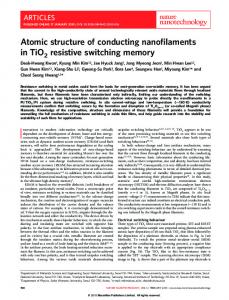
Figure 2. Correlation between lattice parameters, RHEED, and film stoichiometry. (a) X-ray diffraction spectra of SrTiO3/Nb:SrTiO3 films grown with different stoichiometries. The out-of-plane lattice constant increases for TTIP/Sr flux ratios outside of the MBE growth window. (b) In-situ RHEED patterns along the [110] direction. The streakiness of the patterns indicates smooth film surface and the c(4 × 4) reconstruction for TTIP/Sr = 47.8 is characteristic of stoichiometric growth (Ti/Sr = 1). (c) Ti/Sr stoichiometry determined by RBS and correlation with the out-of-plane lattice constant as a function of flux ratio. The grey dots are homoepitaxial calibration growths of SrTiO3 on SrTiO3 substrates.
near-interface region. Specifically, we investigate A-site off-stoichiometric SrTiO3 as an interface layer. This choice was motivated by the ability to grow epitaxial SrTiO3 layers with a well-studied defect chemistry21–25 on doped SrTiO3 substrates, combined with high-quality epitaxial Pt26. Previous studies on non-stoichiometric SrTiO3 involved polycrystalline films27 and metals28,29. This makes them susceptible to a range of defect-related extrinsic effects, but these studies clearly suggested that resistive switching is sensitive to Ti/Sr stoichiometry.
Results
Structural characterization. SrTiO3 films were grown on Nb:SrTiO3 (001) substrates by hybrid oxide MBE30 with five different Ti/Sr ratios. All films thicknesses were between 20 and 30 nm, chosen to avoid strain relaxation for cation off-stoichiometric SrTiO3 films, which have an expanded lattice parameter21,31. Film lattice parameters and stoichiometries, as determined by high-resolution x-ray diffraction and Rutherford backscattering spectrometry (RBS), respectively, are shown in Fig. 2. As can be seen from Fig. 2(a,b), films grown with a TTIP/Sr flux ratio of 47.8 lie in the middle of the MBE growth window31, within which stoichiometric SrTiO3 films are obtained (Ti/Sr = 1) and the film lattice parameter corresponds to that of the substrate, 3.905 Å [TTIP is titanium tetra isopropoxide used to supply Ti]. Stoichiometric films also exhibit a characteristic c(4 × 4) surface reconstruction32 in in situ Scientific Reports | 5:11079 | DOI: 10.1038/srep11079
3
www.nature.com/scientificreports/
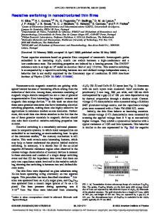
Figure 3. STEM images of nonstoichiometric SrTiO3 films. High-angle, annular dark-field scanning transmission electron microscopy cross-section images for (a) Ti-rich and (b) Sr-rich SrTiO3 films.
reflection high-energy electron diffraction (RHEED), see Fig. 2(b). Ti and Sr-rich films have expanded out-of-plane lattice parameters and RBS indicates that the sample series shown in Fig. 2 spans a wide range of Ti/Sr stoichiometries, between 0.74 and 1.74, see Fig. 2(c). All samples had smooth surfaces, with streaky RHEED patterns and surface roughness