INTL JOURNAL OF ELECTRONICS AND TELECOMMUNICATIONS, 2015, VOL. 61, NO. 1, PP. 101–107 Manuscript received December 18, 2014; revised March 2015. DOI: 10.1515/eletel-2015-0013
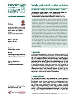
Test Procedures for Synchronized Oscillators Network CMOS VLSI Chip Jacek Kowalski and Michał Strzelecki
Abstract—The paper presents test procedures designed for application-specific integrated circuit (ASIC) CMOS VLSI chip prototype that implements a synchronized oscillator neural network with a matrix size of 32×32 for object detecting in binary images. Networks of synchronized oscillators are recently developed tool for image segmentation and analysis. This paper briefly introduces synchronized oscillators network. Basic chip analog building blocks with their test procedures and measurements results are presented. In order to do measurements, special basic building blocks test structures have been implemented in the chip. It let compare Spectre simulations results to measurements results. Moreover, basic chip analog building blocks measurements give precious information about their imperfections caused by MOS transistor mismatch. This information is very usable during design and improvement of a special setup for chip functional tests. Improvement of the setup is a digitally assisted analog technique. It is an original idea of oscillators tuning procedure used during chip prototype testing. Such setup, oscillators tuning procedure and segmentation of sample binary images are presented. Keywords—neural networks chip testing, synchronized oscillators network, parallel image segmentation; analog-digital VLSI CMOS implementation
I. INTRODUCTION
T
ESTING of analog-digital integrated circuits is much more difficult in comparison with fully digital chips tests. In case of digital chips tests some standard procedures and equipment are available. Unfortunately, such procedures may not be sufficient in the case of analog-digital chip tests. For example, neural networks analog-digital chips require some specific test procedures and special setup designing for chip functional tests. Recently, an increasing number of CMOS realizations of image processing devices can be observed [1]. The main objective of designing and manufacturing integrated circuits implementing tools used in image processing is the speed of performed analysis. Even with the fast development of microprocessors and their functionalities, multicore solutions and the increase in computing performance by making use the power of the GPU, the ASICs are still outperforming all other available solutions. This work is focused on test procedures designed and developed for analog-digital chip prototype implementing 32×32 synchronized oscillator network. The described network The authors are with Institute of Electronics, Lodz University of Technology, Wolczanska 211/215, 90-924 Lodz, Poland; (e-mails:
[email protected],
[email protected]).
chip allows the object detection of binary images in a real time. For example, segmentation and labeling of such images are very important aspects of biomedical image analysis [2,3]. Another realization of an oscillator network chip was presented in [4]. The proposed model is more flexible than the one described in [4] because it provides full dynamic behavior of the oscillator network, as in the original Wang-Terman model [5]. A description of an applied oscillator model can be found in [6]. The paper is organized as follows: Section II describes a synchronized oscillators network CMOS VLSI chip prototype architecture, its operation and cell structure. Section III presents basic chip analog building blocks, their test procedures, simulation and test results. Section IV describes experimental setup for chip functional tests to binary image segmentation tasks. Section V explains an oscillators tuning procedure, which improves image segmentation process. In Section VI results of sample binary images segmentation using the tuned network chip are presented. Finally, our conclusions are presented in Section VII. II. SYNCHRONIZED OSCILLATORS NETWORK CMOS VLSI CHIP ARCHITECTURE A block diagram of the synchronized oscillators network processor is shown in Fig. 1.
Fig. 1. A block diagram of the synchronized oscillators network processor.
The main element of the chip is a matrix of 32 by 32 cells that process the image pixels. Each cell consists of an oscillator CMOS circuit, an excitatory synapse (network weights), and input and output circuits. A block diagram of a
102
J. KOWALSKI, M. STRZELECKI
cell of the synchronized oscillators network is presented in Fig. 2.
Fig. 2. Block diagram of the synchronized oscillators network cell.
An image is fed into the network chip by serial input INP, pixel-by-pixel and line-by-line. Cells are addressed by horizontal and vertical shift registers. The shift registers are controlled by two clocks: CLKH and CLKV. Signals HI and VI are used to synchronize image loading. Control signals are required to write the input image pixels into a chip, as shown in Fig. 3.
OL1-OL32 outputs. During network chip testing, a latter technique (selection of oscillators’ rows) was used for observation and analysis of oscillator output. Thus, the network chip is a mixed signal analog-digital circuit. The global inhibitor and additional oscillator circuits are fully analog. Matrix of 32 by 32 cells containing oscillators and its additional circuits are mainly analog while the shift registers and line decoder are mainly digital circuits. The layout of the synchronized oscillators network chip was designed using Cadence software. The chip was realized in AMIS 0.35µm C035M-D 5M/1P technology by Europractice. Ten prototypes were manufactured. The chip consists of 90952 MOS transistors and occupies 7.9 mm2 of silicon area (2.670 mm × 2.958 mm). Its core without pads has dimensions of 2.3 mm × 2.6 mm. It was encapsulated in a JLCC68 package. The supply current, as measured during image processing, is about 13 mA. The supply voltage is equal to 3 V; thus, the power consumption is about 39 mW. The chip works properly with supply voltages from 2.4 V to 3.6 V. III. TESTS OF BASIC CHIP ANALOG BUILDING BLOCKS A basic analog building block of the chip is CMOS oscillator circuit. Schematic of the oscillator circuit is shown in Fig. 4.
Fig. 4. Schematic of the oscillator circuit.
Fig. 3. Control signals required for input image loading into a chip.
A global inhibitor (GI) circuit is connected to all oscillators in the network. This circuit uses two signals: VGI and XI. Node VGI is activated when at least one oscillator in the network is active. The DGI output signal is a binarized version of VGI and is used for observation of the global inhibitor circuit state. Line XI is used to inhibit all oscillators when GI is active. An additional oscillator, connected to the whole network by weights, is connected to GI only. The oscillator Os was implemented to synchronize the operation of the oscillator network and allows counting the number of recognized image objects. V3S is an output signal of this oscillator. The segmented image objects can be output by a serial digital signal, OUT. This output is controlled in the same way as the INP input by horizontal and vertical registers. It is also possible to observe an activity of a selected oscillator’s row of the network. A 5 to 32 decoder addresses the row. Then, the oscillator’s states are available in digital
Detailed description of the CMOS oscillator circuit can be found in [7]. The oscillator has been implemented in the chip in form of a separate test structure. A schematic of this structure is presented in Fig.5.
Fig. 5. Schematic of oscillator test structure.
TEST PROCEDURES FOR SYNCHRONIZED OSCILLATORS NETWORK CMOS VLSI CHIP
The test structure is composed of the oscillator CMOS circuit, two analog buffers, one digital buffer and input circuit. V1B is an excitatory variable of the oscillator, V2B is an inhibitory state variable and V3B is binarized voltage V1B with a threshold equal to zero. This test structure has been measured using a setup shown in Fig. 6.
103
(transistors M55 – M59) to current. Transistor M57 is working as current source with typical value IG=1µA. Simulated static transfer characteristic Iout(Vin) of input circuit is shown in Fig. 9.
Fig. 6. Setup for measurements of test structure implemented in the chip.
The setup contains the measured test structure TEST1, digital oscilloscope coupled with PC computer using HP-IB interface and a generator for trials of extrinsic synchronization of CMOS oscillator. Oscillograms of CMOS oscillator structure waveforms are shown in Fig. 7.
Fig. 8. Schematic of the input circuit.
In each cell the gates of transistors M51 and M52 (nodes SHi, SVi in Fig. 1) are controlled by two shift registers – horizontal register and vertical register. When transistors M51, M52 are switched on, an input cell pixel voltage value is loaded into gate capacitances of M53 and M54 MOS transistors. If at least one of transistors M51, M52 is switched off the pixel voltage value is stored in M53, M54 transistors gate capacitances and this voltage is converted by OTA (transistors M55 – M59) to current. Transistor M57 is working as current source with typical value IG=1µA. Simulated static transfer characteristic Iout(Vin) of input circuit is shown in Fig. 9.
Fig. 7. Oscillograms of V1B, V2B, V3B waveforms of CMOS oscillator structure.
These waveforms indicate correct operation of the oscillator and are in agreement with computer simulations performed using Spectre software during chip design. A schematic of the input pixel value acquisition circuit is shown in Fig. 8. In each cell the gates of transistors M51 and M52 (nodes SHi, SVi in Fig. 1) are controlled by two shift registers – horizontal register and vertical register. When transistors M51, M52 are switched on, an input cell pixel voltage value is loaded into gate capacitances of M53 and M54 MOS transistors. If at least one of transistors M51, M52 is switched off the pixel voltage value is stored in M53, M54 transistors gate capacitances and this voltage is converted by OTA
Fig. 9. Simulated static transfer characteristic Iout(Vin) of input circuit.
In case of an image inputting Iout=IG=1µA for image objects pixels and Iout=-IG=-1µA for image background. Static transfer characteristics Iout(Vin) of input circuit measured for 7 different chips are shown in Fig. 10.
104
J. KOWALSKI, M. STRZELECKI
were switching off. Lower waveform Iout is output current. It can be observed that output current high state has been stored for about 4 seconds. After that time this current starts transition to low state. IV. LABORATORY SETUP FOR CHIP FUNCTIONAL TESTS To perform image segmentation, an experimental laboratory setup was constructed. Its block diagram is shown in Fig. 12.
Fig. 10. Static transfer characteristic Iout(Vin) of the input circuit (acquired for 7 chips).
As can be noticed from Fig. 10, measured maximum input offset voltage of input circuits is very small when compared to amplitudes of state variables in the oscillator. Mismatch of saturation currents on the left and right side of these characteristics caused by MOS transistor mismatch is rather large. Maximum deviation at the level of 25% when compared to required values has been observed. Current deviation observed in the left branch of input circuit characteristics is not important. It corresponds to not active oscillators since they are connected to image background pixels. Significant differences of Iout current observed in the right branch of discussed characteristic will cause large scatter of frequency oscillations of the oscillators connected to image objects pixels. This may cause problems with active oscillator synchronization, particularly for big image objects (where large number of oscillators should be synchronized simultaneously). In order to minimize this phenomenon, some digitally assisted analog [8] improve technique has been applied. It is an idea of oscillators tuning procedure, described later in Section V. Fig. 11 shows oscilloscope waveforms observed during storing time measurement of the input circuit.
Fig. 11. Oscilloscope waveforms observed during storing time measurement of the input circuit.
Upper waveform Vin represents an input signal. This signal has been delayed after signals SH and SV (Fig. 8) so, that waveform Vin had a high state during transistors M51, M52
Fig. 12. The block diagram of experimental laboratory bench for binary image segmentation.
Our setup consisted of the following elements: • A personal computer (PC); • a universal I/O PCI card (National Instruments NI PCI 7831R), and • a special module containing an integrated circuit of the oscillator network. A PC computer working under Microsoft Windows XP and LabView software (ver. 7.1) was used to program the NI PCI 7831R card. The I/O card has 96 digital reconfigurable inputs/outputs with an operating frequency of 40 MHz. This card also contains an internal FPGA structure. Ten card connectors were configured as outputs and were used to input a binary image to the network chip. The I/O card was connected to a special external test module that contained a chip with an oscillator network. This module also has I/O buffers for input and output data, and row addresses, and circuits designed to control the chip. Polarization currents were used to set the oscillator network weights and the weight of the GI circuit, and to control other oscillator parameters such as a filling ratio of the waveforms representing an excitatory and an inhibitory state variable. It was also possible to switch additional oscillator (Os) circuits and global inhibitor (GI) circuits on and off. The LabView code was used to edit, store, and read a sample binary image from a hard disk. Next, the image was uploaded to the network chip. Image pixels were serially transferred to the chip using synchronization signals HI and VI (Fig. 3). Due to the charge leakage in CMOS structures, the image needed to be loaded repeatedly. The LabView software controlled the refreshing time. This software was stored inside the FPGA structure and allowed the setting of the refreshing period starting from 1 ms in steps of 1 ms. Measurements of chip parameters showed that the refreshing period should be shorter than 4 s (Fig. 11). However, this exceeds the image analysis time, thus there is no need to refresh the loaded image to
TEST PROCEDURES FOR SYNCHRONIZED OSCILLATORS NETWORK CMOS VLSI CHIP
obtain a correct segmentation. After an image was loaded into the network, the oscillators began to oscillate. The oscillator output was obtained for each row, as addressed by the software. Another row could be observed only after a change of the address performed by the I/O card. An appropriate setting of polarization currents that controlled network weights and the GI weight allowed us to find a stable network state where oscillators connected to a given image object were in synchrony, and where oscillator groups representing different objects were desynchronized. V. OSCILLATORS TUNING PROCEDURE During first functional chip tests, some problems with correct detection of thin and long image objects have been observed. This was caused by lack of synchronization of long oscillators chains representing such image objects. Mutual synchronization could not be achieved due to mismatch in oscillation periods in the network. Since the oscillator circuits are analog, MOS transistor mismatch [9,10] caused a mismatch in oscillation frequencies. Some synchronization improvement can be achieved by increasing the power of excitation synapse weights, which can be realized by increasing current IF in the chip. Nevertheless, this method is sometimes ineffective because it causes problems with the desynchronization of oscillator groups connected to different objects. It appears that the best solution is tuning all oscillators to one frequency. To adjust the free frequencies of oscillators in the network, it should be possible to tune each oscillator separately (tuning would affect the oscillator parameters that influence its frequency). Since there are many oscillators in the network, the implementation of separate tuning circuits and tuning mechanisms can consume silicon area and add cost. Therefore, combining image inputting into the network with oscillator tuning seems to be the best solution. The tuning procedure can be realized using analog properties of an input circuit in the oscillator cell. When an image is loaded without tuned oscillators, the current Iout =IG = 1 µA for image objects, and Iout = −I G = −1 µA for the image background. A transitional part of the static transfer characteristic of the input circuit (Fig. 10) has not been used thus far, but it can be used for tuning oscillator frequencies. When an image is loaded with tuned oscillators, the transitional part of the static transfer characteristic of the input circuit is used. Thus, Iout = IG tanh {g(Vin – 1.5 V)} for image objects, and Iout = −IG = −1 µA for the image background. Consequently, the image pixel voltage value Vin for the image object can be tuned to obtain equal free frequencies in all oscillators. The maximum current Iout tuning range is from 1 μA to −1 μA, which corresponds to the effective input voltage Vin from 2 V to 1 V. For an image background, Vin = 0 V. Tuning matrix K is described as follows:
k11 k 21 K = ... k32 1
k12 k 22 ... k32 2
... k1 32 ... k 2 32 ... ... ... k32 32
(1)
Then, assuming that the maximum voltage Vin = 3 V, we have the following relation for image objects:
105
I out i , j = I G tanh{g (3V ⋅ k ij − 1.5V )}
i, j = 1...32
(2)
The oscillator tuning procedure is defined in the following steps: 1.Set oscillator currents IF = 0 (strength of synaptic couplings) and IH = 0 (strength of couplings cells with global inhibitor) to obtain oscillation without excitatory synaptic connections and without global inhibitors (free oscillations). All oscillators in the network should oscillate. If this is not the case, slightly decrease current IE (cell current polarization). 2.Assuming kij = 1 for i,j = 1 ,..., 32, find the oscillator with the smallest frequency fs of free oscillations. 3.Step-by-step, tune the kij coefficient for each oscillator in the network to have all oscillator frequencies as close to frequency fs as possible. The precision of image segmentation by synchronized oscillators network depends on the precision of the aforementioned tuning procedure performance. The control signals required for writing the input image pixels into a chip with oscillator frequency tuning are shown in Fig. 13.
Fig. 13. Control signals required for input image loading into a chip with oscillators frequency tuning.
The difference compared to Fig. 3 is with signal INP. This signal is analog and it includes coefficients from tuning matrix K. Tuning procedure is made only one time for given synchronized oscillators network chip. Each chip is characterized by its own different matrix K. VI. SEGMENTATION RESULTS OF SAMPLE BINARY IMAGE In this section, the results of a sample binary image segmentation using the tuned network chip are presented. An automatically tuned chip was used for image segmentation. After successful automatic tuning using the LabView procedure, the chip was tested on the image segmentation task. An image loaded into the network chip is shown in Fig. 14.
106
J. KOWALSKI, M. STRZELECKI
labeling of each object (image object is represented by all oscillators activated in a given time). Oscillators that belong to the image background do not oscillate (e.g., oscillators 8, 9, 17, Fig. 15). The complete image segmentation occurs when all oscillator groups representing different objects were activated and oscillated. This process takes place in one period of an active oscillator. Thus the segmentation time corresponds to this period length and it is about 1 μs in the case of the image example presented in Fig. 14. The next image loaded into the network chip is shown in Fig. 16.
Fig.14. Sample image loaded into a chip
After loading the image, the segmentation was performed by obtaining oscillators synchronization within any object, and oscillators group desynchronization between oscillators belonging to different object groups. For example, sixteen selected oscillator waveforms for addressed line 14 are presented in Fig. 15.
Fig.16. The second sample image loaded into a chip
For example, oscillators waveforms obtained for line 13 and 17 are presented in Fig. 17 and Fig. 18 respectively.
Fig.15. Selected oscillators output waveforms defined by column numbers for addressed line 14.
The analyzed image contains three objects thus oscillators 3– 7, 11–17, and 21–28 which represent these objects are in synchrony. Due to the channels number limitations of a logic analyzer using for chip analysis, in the Fig. 15 only selected of corresponding oscillator waveforms are shown, e.g., for oscillators 4, 5, 6, 7 (object #1); 12, 14, 15, 16 (object #2), and 21, 22, 23, 25, 28 (object #3) respectively. In fact, these three oscillator groups oscillate with a phase shift (as they represent different objects). As a consequence, waveform analysis of these oscillators, and also the waveforms of oscillators from all other lines (not shown in Fig. 15), allows the detection and
Fig.17. Selected oscillators output waveforms defined by column numbers for addressed line 13.
TEST PROCEDURES FOR SYNCHRONIZED OSCILLATORS NETWORK CMOS VLSI CHIP
107
useful during designing and improving a special setup for chip functional tests. In order to minimize the scatter of frequency oscillations, new kind of digitally assisted analog technique has been applied. It was the original idea of oscillators tuning procedure used during chip prototype testing. It has been demonstrated that testing procedures developed for discussed chip allowed for identification of possible problems of network operation. Finally, implemented oscillator tuning procedure enabled its correct operation. Oscillators have synchronized within an image object while oscillators groups have desynchronized between different image objects. The chip is able to perform fast object detection in binary images in a real time. The processing time of analyzed 32x32 images is about 1 µs. REFERENCES [1]
Fig.18. Selected oscillators output waveforms defined by column numbers for addressed line 17.
It can be observed, that oscillators 17-19 from Fig. 17 (line 13) are in synchrony. Oscillators 9, 10 and 19-24 from Fig. 18 are also synchronized and at the same time desynchronized with two oscillator groups. As a consequence, waveform analysis of these oscillators (and also waveforms of oscillators from all other lines, not shown in Fig. 17 and Fig. 18) allows for detection and labeling of each object from Fig. 16, which leads to segmentation of this image. VII. CONCLUSION Measurements of static transfer characteristics of cell input circuit in 7 distinct chip prototypes gave precious information about their imperfections caused by MOS transistor mismatch. Remaining 3 chips did not work and this fact was detected during measurements of basic building blocks implemented in the chips. Maximum deviation at the level of 25% of saturation currents of these transfer characteristics was a reason of large scatter of frequency oscillations of the oscillators connected to image objects pixels. Large scatter of frequency oscillations of the oscillators caused problems with their synchronization, particularly for big image objects. This observation was very
S. Suh, S. Itoh, S. Aoyama, S. Kawahito, “Column-parallel correlated multiple sampling circuits for CMOS image sensors and their noise reduction effects”, Sensors, 10, pp. 9139-9154, 2010. [2] A. Zalewska, M. Strzelecki, P. Janowski.; E. Brzezińska-Błaszczyk, “Computer analysis of normal and basal cell carcinoma mast cells”, Med. Sci. Monitor, 7, pp. 260-265, 2001. [3] D. Jirak, J. Kriz, M. Strzelecki; J. Yang, C. Hasilo; D. J. White, P. J. Foster, “Monitoring the survival of islet transplants by MRI using a novel technique for their automated detection and quantification”, Magn. Resonan. Mater. Phys. Biol. M., 22, pp. 257-265, 2009. [4] J. Cosp, J. Madrenas, “Scene segmentation using neuromorphic oscillatory networks”, IEEE Trans. Neural Network, 14, pp. 1278-1296, 2003. [5] D. Wang, D. Terman, “Locally excitatory globally inhibitory oscillators network”. IEEE Trans. Neural Network, 6, pp. 283-286, 1995. [6] M. Strzelecki; J. Kowalski; H. Kim, S. Ko, “A new CNN oscillator model for parallel image segmentation”, Int. J. Bifurcation Chaos, 18, pp. 1999-2015, 2008. [7] J. Kowalski , M. Strzelecki, H. Kim, “Implementation of a Synchronized Oscillator Circuit for Fast Sensing and Labeling of Image Objects”, Sensors, vol. 11, no. 4, pp. 3401-3417, 2011, doi:10.3390/s110403401. [8] B. Murmann, "Digitally Assisted Analog Circuits – A Motivational Overview," ISSCC Special-Topic Evening Session (SE1.1), Feb. 2007. [9] M. J. Pelgrom, A. C. J. Duinmaijer and A. P. G. Welbers, “Matching Properties of MOS Transistors”, IEEE Journal of Solid-State Circuits, vol.24, no.5, pp.1433-1439, October 1989,. [10] M. Conti, P. Crippa, S. Orcioni, and C. Turchetti, “Layout-Based Statistical Modeling for the Prediction of the Matching Properties of MOS transistors”, IEEE Transactions on Circuits and Systems—I: Fundamental Theory and Applications, vol. 49, no. 5, pp. 680-685, May 2002.