Aug 29, 2008 - 13, JULY 1, 2008. 1777. The Data Vortex Optical Packet Switched. Interconnection Network. Odile Liboiron-Ladouceur, Member, IEEE, Assaf ...
JOURNAL OF LIGHTWAVE TECHNOLOGY, VOL. 26, NO. 13, JULY 1, 2008
1777
The Data Vortex Optical Packet Switched Interconnection Network Odile Liboiron-Ladouceur, Member, IEEE, Assaf Shacham, Member, IEEE, Benjamin A. Small, Member, IEEE, Benjamin G. Lee, Student Member, IEEE, Howard Wang, Student Member, IEEE, Caroline P. Lai, Student Member, IEEE, Aleksandr Biberman, Student Member, IEEE, and Keren Bergman, Senior Member, IEEE Invited Paper
Abstract—A complete review of the data vortex optical packet switched (OPS) interconnection network architecture is presented. The distributed multistage network topology is based on a banyan structure and incorporates a deflection routing scheme ideally suited for implementation with optical components. An implemented 12-port system prototype employs broadband semiconductor optical amplifier switching nodes and is capable of successfully routing multichannel wavelength-division multiplexing packets while maintaining practically error-free signal 10 12 ) with median latencies of 110 ns. Packet integrity (BER contentions are resolved without the use of optical buffers via a distributed deflection routing control scheme. The entire payload path in the optical domain exhibits a capacity of nearly 1 Tb/s. Further experimental measurements investigate the OPS interconnection network’s flexibility and robustness in terms of optical power dynamic range and network timing. Subsequent experimental investigations support the physical layer scalability of the implemented architecture and serve to substantiate the merits of the data vortex OPS network architectural paradigm. Finally, modified design considerations that aim to increase the network throughput and device-level performance are presented. Index Terms—Interconnection networks (multiprocessor), optical interconnections, packet switching, photonic switching systems, wavelength-division multiplexing.
I. INTRODUCTION EARLY all contemporary large-scale high-performance information systems, including supercomputers, high-capacity data storage, and telecommunications core routers, require high-bandwidth low-latency interconnection networks. In these systems, performance is highly dependent upon the efficiency of vast information exchanges between sometimes thousands of clients (e.g., processors, memory, network hosts).1 It is therefore critical for the interconnect infrastructure to
N
Manuscript received August 15, 2007; revised November 9, 2007. Published August 29, 2008 (projected). This work was supported in part by the National Science Foundation under Grant ECS-0322813 and by the U.S. Department of Defense under Subcontract B-12-664. O. Liboiron-Ladouceur is with McGill University, Montreal, PQ, Canada. A. Shacham is with Aprius Inc., Sunnyvale, CA 94085 USA. B. A. Small, B. G. Lee, H. Wang, C. P. Lai, A. Biberman, and K. Bergman are with the Electrical Engineering Department, Columbia University, New York, NY 10027 USA. Digital Object Identifier 10.1109/JLT.2007.913739 1TOP500
List for June 2006, http:www.top500.org/lists/2006/06
support high-bandwidth low-latency communications that are highly scalable, thus transparently facilitating overall system performance [1]. With the immense growth in data traffic and required computation capacities, conventional electronic interconnection networks utilized for these applications are reaching capacity limits in their ability to meet the increased demands of the surrounding clients. While it is well established that optical data encoding and the utilization of fiber-optic and photonic media possess the potential to provide orders of magnitude more bandwidth at near speed-of-light transmission latencies [2], critical optical technology shortcomings must be addressed. The key challenge for optical interconnection networks is to fully leverage the immense bandwidth of the fiber-optic components through techniques such as wavelength-division multiplexing (WDM) while avoiding the inadequacies of photonic technologies, particularly the absence of robust optical buffers and registers. The data vortex architecture was specifically designed as a packet switched interconnection network for optical implementation; the topology supports large port counts scalable to thousands of communicating terminals. In order to accommodate scalability and to address the problematic absence of reliable dynamic photonic buffers, the conventional butterfly network topology is modified to contain integrated deflection routing pathways. The primary consideration in the architecture’s organization is enabling the optical packets to approach speed-oflight time-of-flight latencies. The switching nodes are therefore designed to be as simple as possible and to contain very little routing logic; in this way, the packets do not sit in buffers while routing decisions are made. These design considerations naturally result in a modular architecture, which is scalable and self-similar in such a way that a small system implementation can predict the performance of significantly larger networks. The data vortex design differs markedly from the conventional approaches to optical packet switched (OPS) networks, in which electronic architectures are often simply mapped into the optical media in a manner that can fail to capitalize on the unique properties of optical transmission. In the data vortex architecture, when processing and routing decisions are required, highspeed digital electronic circuitry is employed in a way that complements the semiconductor optical amplifier (SOA) wide-band photonic switching elements. This allows the high-bandwidth optical payload, which is encoded on multiple wavelengths in
0733-8724/$25.00 © 2008 IEEE
1778
JOURNAL OF LIGHTWAVE TECHNOLOGY, VOL. 26, NO. 13, JULY 1, 2008
2
2
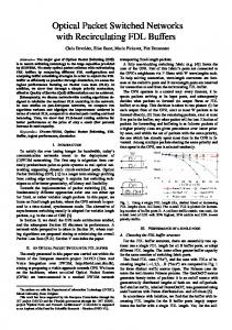
Fig. 1. (a) Illustration of a 12 12 data vortex topology with 36 interconnected (C = 3; H = 4; A = 3) and distributed 2 2 nodes (cylinders). Straight lines are ingression fibers, curved lines are deflection fibers, and dotted lines are electronic deflection signal control cables. (b) The banyan-like crossing pattern shows the deflection path connectivity for each cylinder.
order to maximize transmission capacity, to transparently traverse the network. The data vortex topology [3] was first described in [4] and first investigated in [5]–[7], and its architecture was further analyzed in [8]–[11]. A 12-port data vortex prototype was implemented and its routing performance investigated [12]. The scalability of the physical layer was analyzed and demonstrated in [13] and [14], and further experimental studies of the optical dynamic range and packet format flexibility were performed [15], [16]. Sources of signal degradation in the data vortex were investigated in [17] and [18], and data resynchronization and recovery was achieved using a source synchronous embedded clock in [19]. Extensible and transparent packet injection modules and optical packet buffers for the data vortex were presented in [20]. Finally, alternative data vortex architecture implementations and performance optimization were explored in [21]–[23]. In this paper, we present a comprehensive discussion of the data vortex interconnection network and provide a complete review of the architectural investigations and experimental research. Section II reviews the topology, including a discussion of the deflection routing, network scalability, and node structure. In Section III, the implementation of a fully interconnected 12-port data vortex is presented along with a proposed synchronization approach for recovering short packets. The interoperability of an injection control module with the data vortex is demonstrated as well. Section IV describes the characterization of the physical layer and its quantitative impact on the system
scalability. Section V presents both alternative architectural designs and performance optimization considerations at the device level for next generations of the data vortex interconnection network. II. DATA VORTEX INTERCONNECTION NETWORK The data vortex topology [Fig. 1(a)] integrates internalized virtual buffering with banyan-style bitwise routing specifically designed for implementation with fiber-optic components. The structure can be visualized as a set of concentric cylinders or routing stages, which are cyclic subgroups that allow for deflections without loss of routing progress. Moreover, the hierarchical multiple-stage structure is easily scalable to larger network sizes while uniformly maintaining fundamental architectural concepts [5]. A. Topology The data vortex topology is composed entirely of 2 2 switching elements (also called nodes) arranged in a fully connected, directed graph with terminal symmetry but not complete vertex symmetry. The single-packet routing nodes are wholly distributed and require no centralized arbitration. The topology is divided into hierarchies or cylinders, which are analogous to the stages in a conventional banyan network (e.g., butterfly). The architecture also incorporates deflection routing, which is implemented at every node; deflection signal paths are placed only between different cylinders. Each
LIBOIRON-LADOUCEUR et al.: THE DATA VORTEX OPTICAL PACKET SWITCHED INTERCONNECTION NETWORK
cylinder (or stage) contains nodes around its circumference nodes down its length. The topology conand switching elements, or nodes, tains a total of with possible input terminal nodes and an equivalent number of possible output terminal nodes. The position of , where each node is conventionally given by the triplet . The switching nodes are interconnected using a set of ingression fibers, which connect nodes of the same height in adjacent cylinders; and deflection fibers, which connect nodes of different heights within the same cylinder. The ingression fibers are of the same length throughout the entire system, as are the deflection fibers. The deflection fibers’ height crossing patterns [Fig. 1(b)] direct packets through different height levels at each hop to enable banyan routing (e.g., butterfly, omega) to a desired height and assist in balancing the load throughout the system, mitigating local congestion [5]–[7], [12]. Incoming packets are injected into the nodes of the outermost cylinder and propagate within the system in a synchronous, time-slotted fashion. The conventional nomenclature illustrates packets routing to progressively higher numbered cylinders as moving inward toward the network outputs. During each timeslot, each node either processes a single packet or remains , the th bit of the inactive. As a packet enters node packet header is compared to the th most significant bit in the . If the bits match, the packet innode’s height coordinate through the node’s south output. gresses to node Otherwise, it is routed eastward within the same cylinder to , where defines a transformation node which expresses the above-mentioned height crossing patterns (for cylinder ) [6], [7]. Thus, packets progress to a higher cylinder only when the th address bit matches, preserving the most significant bits. In this distributed scheme, a packet is routed to its destination height by decoding its address in a bitwise banyan manner. Moreover, all paths between nodes progress one angle dimension forward and either continue around the same cylinder while moving to a different height or ingress to the next hierarchal cylinder at the same height. Deflection signals (Fig. 2), discussed further in Section II-B, only connect nodes on adjacent cylinders with the same anto a node at position gular dimension; i.e., from . The paths within a cylinder differ depending upon the level of the cylinder. The crossing or sorting pattern (i.e., the conof the outernections between height values defined by must guarantee that all paths cross from most cylinder the upper half of the cylinder to the lower half of the cylinder; thus, the graph of the topology remains fully connected and the bitwise addressing scheme functions properly. Inner cylinders must also be divided into 2 fully connected (i.e., Hamiltonian) and distinct subgraphs, depending upon the cylinder. Only the may contain connections befinal level or cylinder tween nodes of the same height. The cylindrical crossing must ensure that destinations can be addressed in a binary tree-like configuration, similar to other binary banyan networks. Addressing within the data vortex architecture is entirely distributed and bitwise, similar to other banyan architectures: as a packet progresses inward, each successive bit of the binary
1779
Fig. 2. Schematic representation of the deflection triangle. In order to avoid packet collision at node A, the electrical deflection signal (gray lanes) sent by node B to node C will force the packet at node C to be deflected to node D (black lanes).
Fig. 3. Plot of the number of encountered nodes M as a function of the number of I/O ports . The left curve represents the median number of hops and the right depicts the 99.999th percentile [13].
N
Fig. 4. (a) Switching node structure of the data vortex constructed with couplers (ellipses), filters ( ), isolators (boxed arrows), and a PCB that integrates the control logic components, receivers (O/E), and SOAs.
�
address is matched to the destination. Each cylinder tests only one bit (except for the innermost one); half of the height values permit ingression for 1 values and half for 0 values, arranged in a banyan binary tree configuration. Within a given cylinder ,
1780
nodes at all angles at a particular height (i.e., ) match the )th significant bit value, while the paths guarantee same ( preservation of the most significant address bits. Thus, with each ingression to a successive cylinder, progressively more precision is guaranteed in the destination address. Finally, on the , each node in the angular dimension last cylinder is assigned a least significant value in the destination address so that the packets circulate within that cylinder until a match (A) bits (so-called angle-resolution is found for the last addressing) [12]. As will be discussed in Section II-D, each switching node is bufferless and is designed to check exactly one bit of the destination address, in addition to the packet frame. When the selected address bit matches the value assigned to the node due to its position within the cylinder, the packet is allowed to ingress into the next cylinder on the ingression fiber unless a deflection signal is received. When the selected address bit does not match, or when a deflection signal is received, the packet is routed within the same cylinder on the deflection fiber and the node sends a deflection signal indicating that the next node will soon be busy with the deflected packet. Therefore, every switching element always has an available deflection fiber (east) and ingression fiber (south) used for routing matches. While it may seem wasteful to have twice as many optical paths as necessary, having a guaranteed deflection fiber pathway allows for an extraordinarily simple routing logic that can be executed extremely quickly [12], [24]. The distributed bitwise addressing scheme also helps to ensure that routing decisions do not dominate network latency. No buffers are used, so the network latency can be reduced to approach optical time-offlight. B. Deflection Routing Although packets can originate from either of the two input ports (north or west), recall that the node design is capable of routing only one packet at a time. This fundamental constraint yields a simplistic construction of the node but requires an architectural implementation of internal blocking or deflection. Deflection within the data vortex thus differs from conventional deflection routing topologies that allow for deflection routing at the completion of each discrete node hop. Instead, the data vortex deflection implementation prevents two packets from simultaneously entering the same switching node, and thus colliding, by controlling or blocking one of the two nodes connected upstream of the input ports. Therefore, a packet deflection in cylinder occurs for only two reasons: 1) a packet is deflected in the adjacent cylinder 1, or 2) the packet in cylinder cannot be injected due to a mismatch between its destination address and the node’s height value. A packet that would otherwise ingress into that node on 1 from cylinder (when address bits match) can cylinder thus be required to remain in cylinder when the deflection signal indicates that the desired node is busy. This deflection structure results in “backpressure” from the inner cylinders to the outer cylinders .A deflected packet must traverse two additional node hops before the address matches again, as a consequence of the crossing patterns.
JOURNAL OF LIGHTWAVE TECHNOLOGY, VOL. 26, NO. 13, JULY 1, 2008
The deflection signaling structure incorporates the output and input terminals such that output nodes can receive busy signals from the output queuing subsystem, and the input nodes can transmit similar busy signals to the input interface. Thus, may repackets that attempt input at the first cylinder ceive a signal that indicates that the desired input node is busy; the packet must then be queued to reattempt injection or be discarded. The deflection signal relationship can be represented geometrically as a triangle. In fact, this triangular deflection unit is the fundamental building block of the entire data vortex topology. Only the arrangement of each leg differs from cylinder to cylinder, in accordance with the specific crossing patterns used. The deflection signal’s crossing pattern must be the same as that of the deflection fiber since connections between cylinders do not undergo height translation. In order to maintain correct timing for deflection signaling, particular latency conditions must be satisfied. Since implementations of this architecture avoid buffering within the switching elements, latencies are caused entirely by the optical and electrical (for control signals only) paths’ times-of-flight. To maintain accurate deflection signaling, deflection signals must be transmitted sufficiently early such that the node receiving the deflection signal can direct its packet appropriately. The timing of cylinder 1 containing the node initiating the deflection must therefore precede the timing of cylinder containing the node receiving the deflection signal. Thus, the ingression fibers must be shorter than the deflection fibers by an amount equal to the processing and transmission time of the deflection signal [24]. Consequently, the timing cycles of the inner cylinders precede those of the outer ones. When the aforementioned timing condition is met for the data vortex implementation, global clocking for every switching element is not required. If packets are only injected at timeslots that correspond to the deflection fiber latency, packets will maintain this slotted arrival schedule at every position within the hierarchal topology. Again, recall that no buffers or storage devices are utilized; hence when physical time-of-flight requirements are met, they hold for all packets at each node. C. Scalability of the Topology The data vortex topology exhibits a flexible modular architecture that is scalable to large numbers of input and output ports ( ). To increase the size of the interconnection network, the number of ports can be augmented by increasing the cylinders , angles , or height parameters. Per the topology discussion in Section II-A, the number of ports is defined as the product of the number of angles and heights
(1) The cylinders represent the stages of the data vortex. The cylinder number is defined by and corresponds to one plus the base-two logarithm of , as each routing node consist of two inputs (west and north) and two outputs (south and east)
(2)
LIBOIRON-LADOUCEUR et al.: THE DATA VORTEX OPTICAL PACKET SWITCHED INTERCONNECTION NETWORK
1781
Following the above two equations, a topology can be appropriately designed. The modular architecture enables several possible topologies for the same number of I/O ports. It has been shown that for a given number of ports, a shorter height and greater number of angles provide lower latencies as compared to taller (large ) and narrower (small ) topologies [10]. In optical multistage interconnection networks, an important parameter is the number of routing nodes a packet will traverse before reaching its destination. For the data vortex utiscales lizing 2 2 switching elements, the number of nodes logarithmically with the number of ports [25], [26]
(3) cascaded nodes; generally, Packets will propagate through increases with the network size but is also tightly coupled to the network load. Various scenarios have been simulated to illustrate the effect of the topology and network load [9], [11]. The number of cascaded nodes directly affects on the overall network latency. Due to the deflection characterhas a istic of the network, the number of cascaded nodes non-Gaussian statistical distribution arising from the contention resolution scheme [5], [7]. Simulations of the data vortex as a large-scale switching fabric have shown that for a heavily loaded 10 k 10 k port data vortex implementation, 99.999% of the injected packets propagate through fewer than 58 internal switching nodes with a median hop count of 19 (Fig. 3) [13].
Fig. 5. Timing diagram of the multiwavelength packets with control wavelengths, a clock wavelength, and multiple payload wavelengths.
the innermost cylinder at its destination height, it is routed to the correct output port based on the nodes’ angle parameters . Allocated bits of the header address are typically used for the angle information, but modified decoding logic can be used at the innermost cylinder to reduce the number of channels needed for the address.
D. Packet Self-Routing E. Packet Format The modular architecture of the data vortex and its impressive scalability are made possible by the simplicity of the routing node structure (Fig. 4). The nodes are evenly distributed across the data vortex topology in a manner that facilitates contention resolution while minimizing latency and maximizing throughput. Packets propagate from one of the two inputs of the node (north or west) to one of the two outputs (east or south). Two SOAs are used to select one of the two outputs based on the control information encoded along with the payload data within the optical packet (see Section II-E). The two SOA gates are enabled by laser drivers that are controlled by the electronic decision circuitry internal to each node, producing the routing decisions on a per-packet basis without the need of a central scheduler. To produce the routing decidetect the presence sion, the nodes in the first cylinder of Header 0, the nodes in the second cylinder detect Header 1, and so forth. The frame information is used to validate the presence of a packet in the routing node. If the header bit does not match the user-programmed value for the node, or if the interconnected node in an inner cylinder is busy, the packet is deflected to the next angle in the same cylinder. Here, current is supplied to the east SOA only. If the header bit matches that of the node and no deflection signal is received, then the packet ingresses to the angle in the next cylinder (or stage), as current is supplied to the south SOA only. In this distributed scheme, a packet is routed by decoding its address in a bitwise banyan manner to its destination height. Once a packet reaches
The data vortex architecture utilizes a high-bandwidth multiple-wavelength packet format (Fig. 5). The header address is encoded in the frequency domain through WDM wavelength allocation in order to minimize latency. The implementation of the header address at a lower bit-rate than the payload also facilitates the electronic decoding and interpretation of the routing information. A source-synchronous clock can be encoded on a dedicated wavelength to sample the short packets at the destination node [19]. The remainder of the C-band can be filled with high-bit-rate payload data, since the data vortex is transparent to the optical bit-rate, resulting in very high aggregate bandwidths. The packet timing is precisely defined to maintain contention resolution and network synchronization. The overall slot time corresponds to the time-of-flight between two adjacent nodes such that one packet is contained in only one node at a time. In addition to the packet time, the timeslot includes the dead time and guard time. The dead time distinguishes two temporally adjacent packets and accommodates slight process variations in real-world devices, while the guard time is determined by the finite time required to enable the SOAs. III. DATA VORTEX IMPLEMENTATION A 12-port fully connected data vortex system prototype has been implemented using 36 switching nodes integrated onto six
1782
JOURNAL OF LIGHTWAVE TECHNOLOGY, VOL. 26, NO. 13, JULY 1, 2008
TABLE I DATA VORTEX IMPLEMENTATION WAVELENGTH ASSIGNMENT
printed circuit boards (PCBs) and interconnected by passive optics modules, single-mode fiber, and electronic cables. The design of this system along with improvements for data recovery and packet injection is discussed below. A. Design of a Functional 12-Port Data Vortex In this section, we discuss the design specifications used to demonstrate a fully functional optical packet switched interconnection network. Note that only off-the-shelf components were used in the experimental implementation of the data vortex. ,a In the case of the 12-port data vortex 4-bit header encoded on four header wavelengths is required to address each system output. For a 10 000-port system, 14 headers would be required to route packets individually from each input port to each output port. While the packet is transparently routed through the node, the header address is decoded at each node by filtering a frame wavelength and one cylinder-specific header wavelength. Upon entering the node from either input port, 30% of the input packet’s power is extracted for control signal decoding. The control wavelengths are filtered with 100-GHz optical bandpass filters and directed to photodetectors. The receiver data path is designed to be dc-coupled to accommodate bursty packet arrival. The remainder of the packet power (70%) is routed through a fixed length optical delay line and a 50:50 coupler, which combines the two input ports and splits the optical packet to the two SOAs. The SOAs are followed by isolators in order to mitigate counter-propagating amplified spontaneous emission (ASE) noise. The entire node’s measured latency is 15.8 ns [24]. A packet slot time of 25.7 ns is determined by the total time-of-flight latency between two nodes within the same cylinder and the deflection-timing requirement. Each packet is 22.5 ns long and includes a guard time of 1.6 ns inserted at both the beginning and the end of the packet, yielding a net payload window of 19.3 ns (Fig. 5). A guard time is required for the SOA switching transition time, which is approximately 1 ns. The control information required to route the packets consists of one frame and a 4-bit header. Sixteen payload channels are modulated at 10 Gb/s for 160 Gb/s of aggregated bandwidth. Packet payload bandwidths approaching terabit/second can be straightforwardly achieved by increasing the channel count and modulated data rates (e.g., 25 channels modulated at 40 Gb/s). The selected address field wavelength channels are shown in Table I. In the innermost , a decoding logic uses both header 2 and header cylinder 3 to determine the output port address. In the experimental test bed illustrated in Fig. 6, the payload wavelengths are generated by distributed feedback lasers (DFBs) modulated with a 2 1 pseudorandom bit sequence
at 10 Gb/s and decorrelated with a length of optical fiber by approximately 450 ps/nm. An SOA segments the continuous data stream into packets. Prior to injection in the data vortex, the header and frame information is independently modulated and coupled to the multiwavelength packet to meet the required packet structure (Fig. 5). The timing of all the signals are closely calibrated using the data-timing generator (DTG). At the output port, the packets are preamplified with an erbium-doped fiber amplifier, filtered for a specific payload channel, and converted to an electrical signal through a dc-coupled receiver module. The error rate of the data contained within the individual payload wavelengths of each packet is measured using a bit-errorrate (BER) tester (BERT). The BERT, which enables extensive analysis of the performance of the data vortex network, is externally gated and synchronized with the pulse pattern generator (PPG). To validate the design, routing experiments were performed to demonstrate the correct addressing of packets through the system and to verify the functionality of its contention resolution scheme [3]. All 12 output ports are addressed and contentions are resolved between switching nodes according to the data vortex internal deflection routing mechanism. The system is capable of routing packets with 160 Gb/s (10 Gb/s 16 WDM channels) payloads from any one of the 12 input ports to any one of the 12 output ports. The average (and median) latency for the system is 110 ns, corresponding to five node hops [27]. The emulation of realistic network traffic utilizing a supercomputing interconnection network traffic workload was also demonstrated [28]. The evaluation workload uses processormemory accesses from an application in a SPLASH-2 parallel computing benchmark suite [29]. The methodology captures the behavior of shared memory parallel execution, providing message traffic typically found in a similarly configured multiprocessor system. The simulation results show that all packets are routed correctly; furthermore, appropriate deflections and address decoding are also observed. B. Resynchronization and Recovery Data traffic in interconnection networks such as the data vortex often consists of short and bursty message exchanges. One of the key challenges is resynchronization and recovery of data at the destination node without the use of conventional phase-locked loop designs. In the data vortex, a clock synchronous to the data payload can be embedded in the packet and used as the timing reference at the destination node [19]. The embedded clock avoids the complexity of low-skew clock distribution through large-scale synchronous interconnection networks and simplifies the message recovery circuitry as compared to asynchronous networks. This approach has been demonstrated in the implemented data vortex network by recovering WDM messages routed through five switching nodes. The messages are entirely recovered and processed at the destination node using an embedded clock signal. The clock-to-data skew, defined as the relative timing between the payload and the embedded clock, must remain within the setup-time and hold-time requirements of the deserializer. However, a main contributor to clock-to-data
LIBOIRON-LADOUCEUR et al.: THE DATA VORTEX OPTICAL PACKET SWITCHED INTERCONNECTION NETWORK
1783
Fig. 6. Schematic of the data vortex test bed, including LiNbO modulators (mod), a gating SOA, a pulse pattern generator (PPG), a data-timing generator (DTG), a burst-mode receiver (Rx), and a tunable bandpass filter (�)[12].
skew is group velocity dispersion (GVD). A sampling window, corresponding to over 500 m of interconnected fiber, was measured in [19]. A very large-scale OPS interconnection network such as a 10 k 10 k data vortex would incorporate only about 200 m of interconnected fiber.
C. Node Extension for Packet Injection In an OPS network with an internal contention resolution scheme such as in the data vortex, packet injection must be managed. By extending the routing node, an injection control module (ICM) has been experimentally demonstrated and shown to mediate packet injection into OPS routers such as the implemented 12 12 data vortex network [20]. The basis of the ICM is a reprogrammable nonblocking 2 2 wide-band switching node that controls a feedback fiber delay line (FDL). The module is further composed of SOAs and fast optoelectronic and electronic circuitry that facilitate the dynamic decoding of control signals from the router to manage injection on a packet-by-packet basis (Fig. 7). The module thus operates at the packet timescale and can delay a packet until the router input port is available for injection. The physical complexity of the ICM is independent of the number of packet delay cycles. At each timeslot, the frame bit is extracted from the incoming packet and an electronic busy signal may or may not be received from the router. Based on these inputs, a routing decision is made. In the case where the busy signal is absent, the packet is injected into the router (specifically the outer cylinder nodes of the implemented data vortex). If the busy signal is present, the packet is buffered on the FDL to reattempt injection during the following slot. At the beginning of the next timeslot, another packet may be received at the input port and thus the control circuit must make a routing decision for both packets. If the busy signal is no longer active, indicating that injection is permitted, one packet is injected while the other is delayed. If the router port is still busy, one packet is dropped. The successful implementation of the FDL-based ICM demonstrates that the photonic packet injection module is useful as a functional subsystem for OPS systems such as the data vortex.
IV. DATA VORTEX PHYSICAL LAYER ANALYSIS Although the topology may scale, it does not necessarily follow that the optical physical layer also scales in terms of maintaining end-to-end signal integrity without requiring regeneration. Various effects in the optical domain may limit the true scalability of the data vortex. In this section, we investigate the effects of the physical layer on the optical packets. A. Dynamic Range First, the dynamic range of optical power levels over which the OPS network remains functional is a critical consideration to the physical layer scalability and system robustness. When signal power levels are too low, they are buried in the optical noise floor, yielding poor error-rate performance. At the other extreme, the SOAs may become saturated, leading to enhanced channel crosstalk. In order to determine the system’s robustness to these changes, the optical power of the multiple-wavelength packet is varied uniformly over a wide range of values by inserting a booster SOA before the gating SOA shown in Fig. 6 and by adjusting the gain of these SOAs. The optimal signal power for each payload wavelength is found to be approximately 15 dBm, corresponding to a packet power of approximately 1 dBm for the 16 payload wavelengths. The payload is combined with the five routing wavelengths, each at a power of 13 dBm. At this level, the total SOA input power is about 7 dBm, since around 6 dB of passive optical losses precede an SOA in each node [24], producing a signal power less than the SOAs’ input saturation power of 5 dBm. Payload powers greater than 13 dBm should be avoided, as they will bring the device into the saturation regime, yielding poor BER performance (Fig. 8). For 16 payload wavelengths, the dy(10 ) BER threshold is determined to namic range at a 10 be 6.7 0.3 dB (8.2 0.5 dB), depending on the wavelength of interest (Fig. 8) [16]. B. Packet Format Flexibility Depending on the application and on the type of network behavior, it is important that the network support various packet formats. Two experiments supporting the flexibility of
1784
JOURNAL OF LIGHTWAVE TECHNOLOGY, VOL. 26, NO. 13, JULY 1, 2008
Fig. 7. The injection control module is composed of SOAs, optical couplers, filters, p-i-n photodetectors, optical fiber, and an electronic control circuit [20]. Fig. 9. Power penalty of each of the 16 payload wavelengths for a five-node path through the network [16].
C. Routing Node Power Penalty
Fig. 8. Measured BER versus received power for the 16 payload wavelengths [16]. illustrating the dynamic power range at BERs of 10 and 10
the data vortex packet format have been presented [15], [16]. These confirm that the system can simultaneously route packets containing variable-sized payloads by altering the number of payload wavelengths in the packet and the time duration of the payload data stream. The first experimental demonstration utilizes a variable number of payload wavelengths, while the second utilizes a variable payload time duration while varying the relative location within the timeslot. Specifically, packets with payloads composed of 4, 8, 12, or 16 wavelengths, and time durations of 9.6 and 19.3 ns, are simultaneously routed through a five-node path in the network. Therefore, in a single 25.7-ns timeslot, the data capacity can range from 48 to 384 bytes, corresponding to a net bandwidth in the range of 15–120 Gb/s. The 6-dB variation in power between the packets of 4 and 16 payload wavelengths falls within the previously discussed 6.7-dB dynamic range. As a result, or better were verified for all possible packet BERs of 10 formats (4, 8, 12, or 16 wavelengths and 9.6- or 19.3-ns durations). The demonstrated flexibility very clearly illustrates the transparent nature of the implemented architecture and switching node design.
In many OPS networks, the predominant switching element used is the commercially available SOA, which has a fast switching time, high extinction ratio, broad gain bandwidth, and high potential for integration. The primary function of the SOA is to efficiently and transparently route a broadband packet as well as to compensate for small switching node losses. The SOA, however, introduces ASE noise along with the amplified signal, causing degradation of the optical signal-to-noise ratio (OSNR). In [18], the eye diagram quality factor Q of a typical packet payload channel ( 1547 nm) is shown to degrade from 21.2 dB before injection to 19.0 dB after propagation through a five-node path in the network, which indicates an average decline of approximately 0.4 dB per node. Measurements have also indicated an average OSNR degradation of 2.7 dB per node for a five-node path [16]. Although the SOA’s noise is not expected to increase linearly for a large number of nodes, the precise scaling is difficult to quantify in a concise manner [31]. The total power penalty at the receiver for a five-node path is found to vary between 1.7 and 4.1 dB, measured at a BER of 10 , for all 16 payload wavelengths; the average power penalty is 2.6 dB (Fig. 9). D. Node Cascadability The node cascadability ultimately determines the physical layer size scalability of an SOA-based optical switching network. Node cascadability is influenced by the launched input power of the packets, the power per channel, the number of channels, and the bandwidth across which the channels are distributed. The scalability of a packet-switched optical interconnection network using SOA switching elements has been previously investigated [13]. Using a recirculating loop test-bed environment, the SOA switching nodes were constructed in accordance with the data vortex network architecture. Here, it was shown that BERs lower than 10 can be maintained through 58 node hops (sufficient for a 10 k 10 k port interconnection network) for eight wavelength channels spanning 24.2 nm of
LIBOIRON-LADOUCEUR et al.: THE DATA VORTEX OPTICAL PACKET SWITCHED INTERCONNECTION NETWORK
1785
wavelength variation across a packet’s power spectrum. At each node, the gain/loss varies by less than 1.0 dB across the wavelengths of interest (about 1530–1560 nm), and a packet propagating through a five-node path in the network experiences less than 4.9 dB of net gain/loss variation [16]. F. Polarization Gain Dependence
Fig. 10. Functional bandwidth for eight payload channels versus number of hops. The solid gray line shows simulation results [13].
In order to determine appropriate physical layer constraints, it is important to understand the impact of polarization-dependent gain (PDG), which results from the larger amplification of the transverse electric (TE) mode over the transverse magnetic (TM) mode in bulk active materials. Although polarization dependence in these devices is typically small (generally less than 1 dB), it becomes significant in multistage optical interconnection networks. Again using a recirculating loop test bed with polarization controllers (PCs), it has been shown that the maximum number of cascaded nodes varies by as much as 20 elements for SOA-based designs with PDG of less than 0.35 dB. This corresponds to a 100-fold decrease in the number of interconnected ports of an optical interconnection network such as the data vortex [14]. It hence becomes evident that, for larger network sizes, PDG compensation techniques are necessary to minimize the dramatic shift in performance. G. Timing Accuracy Effect