Education of China, Tsinghua University, Beijing 100084;. 3. Biomanufacturing and Rapid Forming Technology Key Laboratory of Beijing,. Tsinghua University ...
The effect of scan pattern on microstructure evolution and mechanical properties in electron beam melting Ti47Al2Cr2Nb Wenjun Ge1, 2, 3, Feng Lin1, 2, 3, Chao Guo1, 2, 3 1. Department of Mechanical Engineering, Tsinghua University, Beijing 100084; 2. Key Laboratory for Advanced Materials Processing Technology, Ministry of Education of China, Tsinghua University, Beijing 100084; 3. Biomanufacturing and Rapid Forming Technology Key Laboratory of Beijing, Tsinghua University, Beijing 100084. REVIEWED Abstract Ti47Al2Cr2Nb alloy square samples with dimensions of 20mmh20mmh5mm were fabricated by electron beam selective melting. In order to study the effect of electron beam scan pattern on the microstructure evolution, three different scan patterns were employed: S-shaped scan line, Z-shaped scan line and interlayer orthogonal S-shaped scan line. Microstructural and chemical analyses were conducted using optical microscopy, scanning electron microscopy and energy differential system. It is worth noting that the element Al loss rate was about 8% under different process parameters. As a result, the microstructures of EBSM Ti47Al2Cr2Nb samples were composed of columnar β grains, α/α2and α2/γ lamellar. Tensile tests were carried out to understand the mechanical properties to the corresponding microstructures. Ultimate Tensile Stress (UTS)at room temperature is much lower than that at a high temperature. Introduction Intermetallic TiAl alloys are gaining more and more attentions because of the outstanding properties such as the low density(3.9-4.2g.cm-3), high strength and high-temperature oxidation and creep resistance. TiAl alloys appear as promising high-temperature materials used in automotive, energetic and aerospace industries. However, TiAl alloys exhibit poor processing plasticity at room temperature which
500
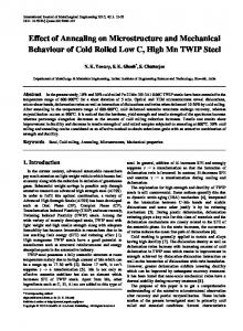
leads to poor workability at room temperature. Recently, electron beam selective melting (EBSM) has been studied as a feasible method for manufacturing Ti6Al4V and Ti-Al intermetallic [1-3].Electron beam selective melting is one of the additive manufacturing methods with high fabrication quality. Compared to laser manufacturing [4], electron beam selective melting has higher energy density and scan speed which reduce the time and cost of manufacturing. In addition, EBSM technology has advantages of vacuum fabrication environment in fabricating impurity sensitive and highly reflective materials. Therefore it is of particular interest to investigate the EBSM fabrication of intermetallic TiAl components. TiAl alloys have four typical microstructures and the mechanical properties of TiAl alloys are strongly dependent on the microstructure. In electron beam selective melting, columnar crystals trend to be formed because of the high cooling rate and big temperature gradient. The scan pattern has an effect on the temperature gradient, which would further influence the growth of grains and the mechanical properties. This work investigated the microstructures and resultant mechanical properties of samples fabricated employing three different scan patterns, namely S-shaped scan line, Z-shaped scan line and interlayer orthogonal S-shaped scan line (also called interlayer cross scan line). Experiments In this study, square samples were fabricated by electron beam selective melting from pre-alloyed Ti47Al2Cr2Nb powders with particle sizes between 45 and 150 μm(Fig.1). The powder had a chemical composition (in atomic percentage)of46.51% aluminum, 0.02% niobium, 0.02% chromium, balance titanium. The powder exhibits fine surface and highly spherical shape, and little satellite particles are also visible.
501
Fig.1microscopic view of Ti47Al2Cr2Nb powder
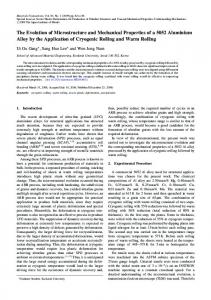
Fig.2 shows the schematic diagram of EBSM-250 system designed by Tsinghua University. Compared with commercial EBSM equipment, EBSM-250 system can mix two kinds of powder together and then fabricate functionally gradient materials. In the system, electron beam is generated in the electron gun and accelerated at a voltage of 60KV. The electron beam is focused by focusing coil and scanned by deflection coil to preheat and selectively melt powders layer-by-layer. Filament Cathode
-70kV
Gate (0~-1500V to the cathode) Electron beam gun
Anode
Focusing coil
Deflection coil
Vacuum chamber
Powder storage Electron beam Powder spreader Parts Vertical piston
Fig.2 schematic diagram of EBSM-250 system designed by Tsinghua University
In this work, a preheating beam current of 20mA, a melting beam current of 6mA a hatching distance of 0.1mm and a scan speed of 0.2m/s were employed. Components were built directly on 316L stainless steel base plate dimensioning 10mm in thickness and 90mm×90mm in area. Before fabrication, the stainless steel base plate was preheated to about 800ć.The effect of scan pattern on microstructure and mechanical properties were investigated systematically by varying the scan
502
pattern. The three scan patterns used are shown schematically in Fig.3.
%XLOG� GLUHFWLRQ
(a) Z-shaped scan line
(b) S-shaped scan line
%XLOG� GLUHFWLRQ
(c)Interlayer cross S-shaped scan line Fig.3 Scan patterns used in EBSM process
The fabricated specimens were cut along the deposition direction employing electron-discharge machining and then mounted, ground, polished and etched. Kroll's reagent was used to etch the samples. The microstructure of EBSM samples was characterized using optical microscopy and scanning electron microscopy. Crystallographic orientation was examined by electron backscattered diffraction (EBSD). Flake samples were taken for tensile tests at different temperatures on a universal material tension machine. Results and discussion 3.1 Aluminum loss As reported before, element Al loss is dependent on energy input and beam current. High energy input and beam current will result in high loss rate. Carolin Korner[5]found that line energy of 1.1J/mm and beam current of 9.2mA cause a Al loss of about 4% while line energy of 0.7J/mm and beam current of 3.5mA reduce the loss to about 1at.%.Denis Cormier et al[6] fabricated Ti-47Al-2Cr-2Nb samples employing a scan speed of 0.1m/s and a beam current of 13mA, and found approximately 6.1%
503
of the aluminum vaporized during the process. In this paper, specimens were fabricated employing a beam current of 6mA, a scan speed of 0.1m/s and a layer thickness of 0.1mm under three different scan patterns. Energy-dispersive spectroscopy (EDS)was employed to conduct the element analyses and the results are shown as Table-1.After the comparison with the original atomic percentage of the powder, it is demonstrated that the element loss rate of Al varies from 8% for S-shaped scan line to 6% for Z-shaped scan line. Table-1 Element analyses results (at. %) S-shaped
Cross S-shaped
Z-shaped
Al
38.15
39.20
40.13
Ti
57.32
56.16
55.32
Cr
1.58
1.76
1.65
Nb
2.95
2.88
2.90
The formation and transformation of the microstructure are strongly influenced by Al loss, especially high losses. In light of the Ti-Al two-phase diagram, the solidification reactions altered significantly with the percentage of Al. (1)Al