The Influence of Growth Temperature on Oxygen Concentration in GaN Buffer Layer ... GaN layers were grown on sapphire substrates in AIX 200/4 RF-S metal ...
Mater. Res. Soc. Symp. Proc. Vol. 1068 © 2008 Materials Research Society
1068-C03-09
The Influence of Growth Temperature on Oxygen Concentration in GaN Buffer Layer Ewa Dumiszewska1,2, Wlodek Strupinski1, Piotr Caban1,3, Marek Wesolowski1, Dariusz Lenkiewicz1,2, Rafal Jakiela1,4, Karolina Pagowska5, Andrzej Turos1,5, and Krzysztof Zdunek2 1 III-V Epitaxy Department, Institute of Electronic Materials Technology, Wolczynska 133, Warsaw, 01-919, Poland 2 Faculty of Materials Science, Warsaw University of Technology, Woloska 141, Warsaw, 02507, Poland 3 Institute of Microelectronics and Optoelectronics, Warsaw University of Technology, Nowowiejska 15/19, Warsaw, 00-665, Poland 4 Institute of Physics, Polish Academy of Sciences, Lotnikow 32/46, Warsaw, Poland 5 Soltan Institute for Nuclear Studies, Swierk/Otwock, 05-400, Poland ABSTRACT The influence of growth temperature on oxygen incorporation into GaN epitaxial layers was studied. GaN layers deposited at low temperatures were characterized by much higher oxygen concentration than those deposited at high temperature typically used for epitaxial growth. GaN buffer layers (HT GaN) about 1 µm thick were deposited on GaN nucleation layers (NL) with various thicknesses. The influence of NL thickness on crystalline quality and oxygen concentration of HT GaN layers were studied using RBS and SIMS. With increasing thickness of NL the crystalline quality of GaN buffer layers deteriorates and the oxygen concentration increases. It was observed that oxygen atoms incorporated at low temperature in NL diffuse into GaN buffer layer during high temperature growth as a consequence GaN NL is the source for unintentional oxygen doping. Keywords: A1. MOVPE; A3 Gallium Nitride.; B1.Oxygen; INTRODUCTION Gallium nitride plays a significant role in optoelectronic and high-power, high frequency devices industry. Lack of commercially available free standing GaN substrates makes it necessary to use alternative ones such as sapphire (Al2O3), silicon carbide (SiC) or silicon. As the result, GaN layers grown on sapphire by the most commonly used method - metalorganic vapor phase epitaxy (MOVPE) are characterized by high oxygen concentration [1]. Oxygen in GaN layers influences n-type background conductivity and may be responsible for threading dislocation behavior [2,3]. Unfortunately, the origin of oxygen atoms is still not well understood. It was suggested that it was incorporated during the growth [3] or comes from sapphire substrate [4]. There are also numerous works indicating interactions between oxygen atoms and dislocations [3,5]. Liliental-Weber et al. [6] showed the increased nanopipes density at elevated oxygen content. Cherns et al. [7] claimed that oxygen may be responsible for electrical activity of dislocations. Our recent results also indicate that interaction between dislocations and oxygen atoms influences device performance [8]. There is a strong correlation between oxygen concentration and carrier concentration in high temperature (HT) GaN, i.e. the larger oxygen content, the higher carrier concentration. The aim of this work was the search for the principal source of oxygen in HT GaN. The effects of the growth temperature on oxygen concentration in gallium nitride layers were studied. We have proved that the low growth temperature of the nucleation layer (deposited at 550 ºC) is decisive for oxygen content in HT GaN.
EXPERIMENTAL GaN layers were grown on sapphire substrates in AIX 200/4 RF-S metal organic vapor phase epitaxy low-pressure reactor. The source gases were trimethylgallium (TMGa, 10 ml/min), and ammonia (NH3, 2000 ml/min). Hydrogen flow of 20 ml/min of through TMGa bubbler and 2000 ml/min of NH3 was applied. The reactor pressure and temperature were 250 mbar and 1140°C respectively. High purity hydrogen was used as a carrier gas.
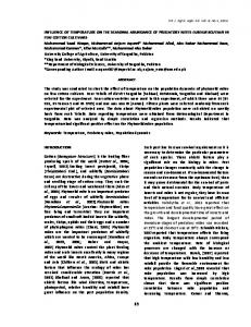
b)
a)
o
o
GaN – 1140 C - 1µm
GaN – 600 C - 1µm
o
GaN – 700 C - 1µm o
GaN – 700 C - 1µm
o
GaN – 800 C - 1µm o
GaN – 1140 C – 1µm
o
GaN – 900 C - 1µm GaN nucleation layer
o
GaN – 1140 C – 1µm Sapphire substrate GaN nucleation layer
Sapphire substrate
Fig.1. Test structures for oxygen incorporation study. Different layer sequences were grown on sapphire substrate: a) GaN NL, HT GaN layer (1140oC), low temperature GaN layer (700oC), HT GaN layer (1140oC); b) GaN NL, HT GaN layer (1140oC), four GaN layers grown at 900oC-600oC.
Two epitaxial structures showed in Figs. 1a and b were deposited at various temperatures. First one, cf. Fig. 1a, consisted of three layers subsequently deposited at 1140°C at 700°C and finally again at 1140°C. The second structure, cf. Fig. 1b, is composed of GaN HT layer and four GaN layers grown at the temperatures deceasing from 900°C to 600°C with 100oC steps without stopping the growth. Thickness and crystalline structure of NL and overgrown GaN epilayers was determined by RBS/channeling [9]. Oxygen concentration in these structures was measured by SIMS.
RESULT AND DISCUSSION
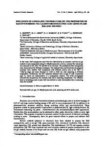
3000
d=30 nm d=50 nm d=70 nm
2500
Yield
2000
1500
1000
500
0 200
400
600
800
1000
1200
1400
Energy [keV] Fig. 2. Aligned RBS/channeling spectra recorded for about 1 µm thick HT GaN layers deposited on NL with various thickness.
Influence of the NL thickness on the grown layers structure was studied by RBS/channeling using 1.7 MeV 4He ions. GaN layers of about 1 µm thickness were grown on NL of varying thickness. As shown in Fig. 2 two regions can be distinguished in the aligned channeling spectra. The first one is delimited by pronounced peaks located in the vicinity of GaN/sapphire interface (around 600 keV of backscattered ion energy) and correspond to the large defect agglomeration, which is composed of defects generated by layer/substrate lattice misfit and remnants of polycrystalline NL. The second region (energies above 900 keV) reflects the top part of layers approximately 600 nm thickness. By applying appropriate evaluation methods layer thickness and their crystalline quality can be determined [10]. Very low scattering yield of aligned spectra in this region amounting to less than 2% of that for random spectra (not shown here) reveal very good quality of layers. Two conclusions can be drown from spectra shown in Fig. 2: (i) interface defect agglomeration grows with increasing thickness of NL, (ii) there is no visible influence of this effect on the top layer crystalline quality. Figs. 3a and b show SIMS profiles recorded for structures shown in Figs. 1. a) and b), respectively. SIMS profile in Fig. 3a clearly demonstrates that there is an enhanced oxygen incorporation into GaN at low temperatures. Oxygen concentration in the middle layer deposited at 700°C contains about two orders of magnitude higher oxygen concentration than the HT GaN layers. SIMS profile showed on fig. 2 b) confirmed this behavior. First layer deposited at 1140°C is characterized by the lowest oxygen concentration. With continuing growth at decreasing temperature oxygen concentration in the subsequent GaN layers increase. Finally, the layer deposited on the top of the structure at 600oC contains the highest oxygen concentration.
10
20
1200
21
10
b)
10
19
1000 10
18
10
17
10
16
900
800
3
1100
Oxygen concentration [ at/cm ]
Oxygen concentration [ at/cm3 ]
a) 20
10
19
10
18
10
700 17
0
1
2
3
4
5
10
0
Depth [ µm ]
1
2 3 Depth [ µm ]
4
5
Fig. 2. Oxygen depth profiles recorded with SIMS for structures shown in Figs. 1. a and b, respectively.
Fig. 4 shows the oxygen depth profile for GaN buffer layers deposited on GaN NL with various thickness. Oxygen concentration in GaN buffer layers increases with increasing thickness of GaN NL. Although the effect is not so pronounced as in the case of growth temperature the overall tendency seems to be confirmed.
3
Oxygen concentration [ at/cm ]
10
21
10
20
10
19
10
18
10
17
10
16
0,0
20 nm 30 nm 50 nm 70 nm
0,5 Depth [ µm ]
1,0
Fig. 4. Oxygen depth profile recorded with SIMS for GaN buffer layers deposited on GaN nucleation layer with various thickness.
Growth temperature has an important influence on properties of GaN epitaxial layers. At low temperatures oxygen incorporation into GaN is facilitated. Most probably the source of oxygen are the trace contaminations of nitrogen precursor: ammonia. Our results confirm observations of Chung and Gershenzon [5] that oxygen can be easily incorporated into GaN at low the temperatures.
Another source of oxygen is the low temperature NL. Our RBS/channeling analysis demonstrated that crystalline quality of the GaN buffer layer/GaN NL interface depends on the thickness of GaN nucleation layer: with increasing thickness of NL the crystalline quality of the interface region strongly deteriorates. This is reflected by the size of defect agglomeration in the vicinity of interface (cf. fig. 2). Also oxygen concentration in HT GaN layer increases with the NL thickness. Since the interface region is the most defective part of a GaN layer it provides a variety of easy paths for oxygen diffusion during the high temperature growth. This is supported by observations of Pearton et al. [11] who proved that the expanded regions around dislocations are easy paths for impurities diffusion. As a consequence, GaN buffer layer deposited on the thickest GaN NL is characterized by the highest oxygen concentration (cf. Fig. 4). One can conclude that nucleation layers deposited at low temperature are effective source of oxygen in GaN buffer layer. At high temperatures large amounts of oxygen incorporated in GaN NL can easily diffuse into GaN buffer layer during its growth. SUMMARY In summary, we have studied influence of the growth temperature on oxygen incorporation into GaN layer. Two structures consisted of GaN layers deposited at various temperatures were grown. Layers deposited at lower temperatures were characterized by the higher oxygen concentration. The most probable oxygen source is due to the contamination of precursor gases. Analysis of GaN buffer layers grown on GaN NL with various thickness revealed the presence of large defect agglomerations in the vicinity interface GaN buffer layer/GaN NL that grows with increasing NL thickness. They form easy paths for diffusion of oxygen accumulated in NL. Consequently, oxygen concentration in GaN layers increases with increasing NL thickness. REFERENCES [1] C. G. Van de Walle, J. Neugebauer, J. Appl. Phys. 95, 3851 (2004). [2] M.E. Hawkridge, D. Cherns, Appl. Phys. Lett. 87, 221903 (2005). [3] M. E. Hawkridge, D. Cherns, T. Myers, Appl. Phys. Lett. 89, 251915 (2006). [4] G. Popovici, W. Kim, A. Botchkarev et al., Appl. Phys. Lett. 71, 3385 (1997). [5] B-C.Chung, M. Gershenzon, J. Appl. Phys. 72, 651 (1992). [6] Z. Liliental–Weber, Y. Chen, S. Ruvimov et al., Phys. Rev. Lett. 79, 2835 (1997). [7] D. Cherns, C. G. Jiao, H. Mokhtari, J. Cai, and F. A. Ponce, phys. stat. sol. (b) 234, 924 (2002). [8] E. Dumiszewska, W. Strupiński, K. Zdunek, J. of Superhard Materials 29, 174 (2007). [9] L.C. Feldman, J.W. Mayer: Ion Channeling in Materials Science, Academic Press, New York 1984 [10] L. Nowicki, A. Turos, R. Ratajczak, A. Stonert, and F. Garrido, Nucl.Instr. and Meth. B240, 277 (2005). [11] S. J. Pearton, H. Cho, J. R. LaRoche et al., Appl. Phys. Lett. 75, 2939 (1999).