SERBIAN JOURNAL OF ELECTRICAL ENGINEERING Vol. 11, No. 1, February 2014, 73-84 UDC: 530.145:621.37
DOI: 10.2298/SJEE131213007T
The Optimal Dimensions of the Domain for Solving the Single-Band Schrödinger Equation by the Finite-Difference and Finite-Element Methods Dušan B. Topalović1,2, Stefan Pavlović3, Nemanja A. Čukarić1, Milan Ž. Tadić1 Abstract: The finite-difference and finite-element methods are employed to solve the one-dimensional single-band Schrödinger equation in the planar and cylindrical geometries. The analyzed geometries correspond to semiconductor quantum wells and cylindrical quantum wires. As a typical example, the GaAs/AlGaAs system is considered. The approximation of the lowest order is employed in the finite-difference method and linear shape functions are employed in the finite-element calculations. Deviations of the computed ground state electron energy in a rectangular quantum well of finite depth, and for the linear harmonic oscillator are determined as function of the grid size. For the planar geometry, the modified Pöschl-Teller potential is also considered. Even for small grids, having more than 20 points, the finite-element method is found to offer better accuracy than the finite-difference method. Furthermore, the energy levels are found to converge faster towards the accurate value when the finite-element method is employed for calculation. The optimal dimensions of the domain employed for solving the Schrödinger equation are determined as they vary with the grid size and the ground-state energy. Keywords: Schrödinger equation, Finite-difference method, Finite-element method, Semiconductor quantum well, Quantum wire, Nanowire.
1
Introduction
Semiconductor nanostructures have been in the focus of research for the last few decades, with promising applications in electronics and photonics [1-3]. Techniques of molecular beam epitaxy and metalorganic vapor phase epitaxy allow fabrication of layered structures of almost arbitrary composition and thickness. However, most attention has been devoted to the GaAs/(Al,Ga)As system, since GaAs and (Al,Ga)As are almost lattice matched, therefore no restrictions are imposed on thickness of the layers of GaAs and (Al,Ga)As. 1
School of Electrical Engineering, Bul. kralja Aleksandra 73, 11000 Belgrade, Serbia; E-mails:
[email protected];
[email protected];
[email protected] University of Belgrade, Vinča Institute of Nuclear Sciences, Serbia; E-mail:
[email protected] 3 Department of Physics, University of Antwerp, Belgium; E-mail:
[email protected]
2
73
D. Topalović, S Pavlović, N. Čukarić, M. Tadić
Furthermore, for the mole fraction of GaAs less than 0.4, (Al,Ga)As is a direct band gap semiconductor, therefore the GaAs/(Al,Ga)As nanostructures are suitable for fabrication of lasers. The electron states in the GaAs/(Al,Ga)As quantum wells might be modeled by the single-band Schrödinger equation. To adopt this approach, quantum well layers should be thicker than about 2 nm, otherwise influence of the interfaces could be quite large [1, 2]. Besides layered nanostructures, the single-band Schrödinger equation has been successfully employed to model the electron states in semiconductor quantum wires and quantum dots [4]. A novel technique to grow nanowires is the VLS (vapor-liquid-solid) process, which has been employed to create freestanding and core-shell nanowires with a nearly cylindrical shape [5]. Because of the axial symmetry of these quantum wires, the single-band Schrödinger equation could be simply solved in the cylindrical coordinate system. Furthermore, the potential well in these quantum wires is a few eV deep, therefore the electrons could be regarded to be confined in an infinitely deep quantum well. The secular equation can be derived for only a few confining potentials in nanostructures. The notable examples are the potential of the rectangular semiconductor quantum well, the potential of the one-dimensional (1D) linear harmonic oscillator (LHO), and the isotropic 2D LHO model. For the general case, however, numerical methods should be employed to solve the single-band Schrödinger equation [6 – 10]. Two such cases are nanostructures exhibiting compositional intermixing [11, 12] and modeling the effects of charge redistribution from the well to the barrier, which should be considered by jointly solving the Schrödinger and the Poisson equation in a self-consistent manner [6]. The Schrödinger equation can be numerically solved by the finite difference method (FDM) [6, 7] and the finite element methods (FEM) [8 – 10]. They are both relatively easy to implement, the accuracy of the computed energies can be controlled by varying the grid size and the dimension of the solution domain. Furthermore, a nonuniform grids can be adopted in both models. However, it is not a priori clear which of the two methods is more effective for solving the Schrödinger equation. The present paper presents the numerical procedures for solving the singleband Schrödinger equation in the GaAs/(Al,Ga)As quantum wells and quantum wires. The calculations are based on both the FDM and FEM. The deviations of the energy levels computed by means of the two methods from the analytical results are analyzed as they vary with the grid size. For both the analyzed numerical methods the optimal dimensions of the solution domains are determined. Moreover, variations of the numerical error of the ground state energy levels in the quantum wells and quantum wires with both the grid size and the ground state electron energy are determined and analyzed. 74
The Optimal Dimensions of the Domain for Solving the Single-Band Schrödinger…
2
Theoretical and Numerical Methods
GaAs and (Al,Ga)As have large energy gaps, thus the electron states in the conduction band of the GaAs/(Al,Ga)As quantum wells can be computed by the single-band Schrödinger equation
−
=2 d ⎛ 1 d ⎞ ⎜ ⎟ ψ ( z ) + Veff , k|| ( z )ψ ( z ) = E ψ( z ) . 2 dz⎝m dz⎠
(1)
Here m denotes the effective mass which varies along the z axis, and Veff ,k& ( z )
is the effective confining potential =2 2 k|| , (2) 2m where V0 ( z ) has the rectangular shape if it arises from the conduction-band offset, and could be described by the potentials of the linear harmonic oscillator (LHO) and the modified Pöschl-Teller potential to take into account the effects of compositional intermixing. The term = 2 k&2 / 2m in equation (2) describes free motion of the electron in the quantum-well plane, which takes place with the inplane wave vector k& . By solving equation (1) for different k& values the
Veff ,k|| ( z ) = V0 ( z ) +
subband dispersion relations E (k& ) are determined. In a cylindrical quantum wire the Schrödinger equation reads
−
=2 1 d ⎛ 1 d ⎞ ⎜ ρ ⎟ χ(ρ) + Veff , kz ( ρ ) χ(ρ) = E χ(ρ) . 2 ρ dρ ⎝ m dρ ⎠
(3)
Here, k z denotes the longitudinal wave number describing the electron free motion along the z direction, and m = m(ρ) , where ρ is the radial coordinate of the cylindrical coordinate system. Therefore, the effective potential has the form
Veff ,kz ( z ) = V0 ( z ) +
=2 l 2 =2 2 + kz . 2m ρ2 2m
(4)
Even though the effective mass values in GaAs and (Al,Ga)As differ, we assumed the approximation of the spatially constant effective mass, for which we adopted the value in GaAs, where the electron is mainly localized. Furthermore, for the constant effective mass, the depth of the effective potential well does not depend on the wave vector k& or k z , therefore it suffices to analyze the accuracy of the calculations for k& = 0 and k z = 0 . For this case, the Schrödinger equation for the planar quantum well has the form −
=2 d 2 ψ + V0 ( z )ψ ( z ) = E ψ ( z ) , 2m d z 2 75
(5)
D. Topalović, S Pavlović, N. Čukarić, M. Tadić
whereas for the cylindrical quantum wire ψ = χ ρ is substituted in equation (3) to remove the term inversely proportional to ρ , thus the Schrödinger equation has the form −
=2 ⎛ d2 1 ⎛ 1 2 ⎞⎞ ⎜ 2 + 2 ⎜ − l ⎟ ⎟ ψ + V0 (ρ)ψ = E ψ . 2m ⎝ d ρ ρ ⎝ 4 ⎠⎠
(6)
In the FDM, equations (5) and (6) are solved by replacing the second derivative with ψ − 2ψ i + ψ i −1 ψ′′(u ) ≅ i +1 . (7) h2 Here, h is the step of the uniform grid, and ψ i = ψ (u = ih) . Hence, at each grid point the differential equation (5) is replaced with the difference equation
−ψ i +1 + ( Di − λ ) ψ i − ψ i −1 = 0, i = 1, 2,..., N ,
(8)
where: 2m 2 (9) h Ui + 2 , =2 2m λ= 2 E. (10) = A similar procedure is adopted to compute the quantum-wire states by the FDM. On the other hand, in the finite element calculations [8] the unknown wave function is expanded into the shape functions f j (u ) Di =
n
ψ (u ) = ∑ a j f j (u ) ,
(11)
j =1
where a j ’s are the coefficients of expansion. For simplicity, the first-order (linear) shape functions are employed. Multiplying equation (11) by f i ( z ) and subsequently integrating (Galerkin approach) equation by parts gives Ha = ESa , (12) where a is the vector of the expansion coefficients. The matrix elements of H and S are given by
H ij =
d d =2 d fi d f j d z + ∫ fi ( z )U 0 ( z ) f j ( z )d z , 2m −∫d d z d z −d
(13)
d
Sij =
∫
fi ( z ) f j ( z ) d z ,
−d
76
(14)
The Optimal Dimensions of the Domain for Solving the Single-Band Schrödinger…
where d = D / 2 is the half-width of the solution domain, and D is the domain full width. For quantum wires, following the similar procedure a similar set of equations is derived from equation (6).
3
Computer Implementations
In our calculations, the value of electron effective mass is m = 0.067m0 , half-width of the rectangular quantum well equals w = 10 nm, dimension (width or diameter) of the solution domain equals D = 40 nm, and height of the rectangular potential well amounts to V0 = 0.3 eV in both the planar and the cylindrical geometry. The accuracy of the employed numerical methods is quantified by the error of the electron ground state energy, ΔE = Enum − Eacc , (15)
where Enum and Eacc are the computed and the accurate energy values. If the domain size D is kept fixed and the number of the subdomains N varies, the error of the ground state energy in a rectangular quantum well oscillates, as Figs. 1 and 2 show for the planar and the cylindrical geometry, respectively. The displayed oscillations originate from varying the position of the grid point which is closest to the heterojunction boundary. If we denote the number of this point as nw , the actual width of the quantum well in our numerical calculations is wnum = nw D / N . For a certain value of N , the value of wnum might be close to the quantum well half-width w . However, when N increases to N + 1 , wnum could become much smaller than w , which leads to increase in the calculated eigenenergy. If N increases further, the value of wnum could again approach w , therefore the energy decrease. We note that wnum is not allowed to exceed w in our calculations. Furthermore, we define the numerical half-width of the quantum well as wnum = w − fh , (16) where 0 ≤ f ≤ 1 . According to (16) wnum → w when N increases, which explains why amplitude of the oscillations shown in Figs. 1 and 2 decreases. Interestingly, the oscillations of the ground energy level computed by the FEM have smaller amplitude in both the planar and cylindrical geometry. It is due to the fact that the energy value computed by the FEM depends on integrals, therefore the dependence of the matrix elements of the Hamiltonian on N is smoothed out, even when the position of the well-barrier boundary is not precisely determined. Therefore, the FEM was found to be more robust than the FDM to solve the Schr dinger equation. 77
D. Topalović, S Pavlović, N. Čukarić, M. Tadić -3
x 10 3 FDM FEM
ΔEFD1 , Δ EFEM1 [eV]
2
1
0
-1
-2
10
15
20
25
30 N
35
40
45
50
Fig. 1 – The error of the computed electron ground state energy in a rectangular quantum well as function of the number of the grid points. The oscillatory curve depicted by blue color is the result obtained by the FDM, while the green line shows the result of the FEM calculations. -3
2
x 10
FDM FEM
1
Δ EFD1, ΔEFEM1 [eV]
0 -1 -2 -3 -4 -5 -6 -7
10
15
20
25
30 N
35
40
45
50
Fig. 2 – The error of the computed electron ground state energy in a cylindrical quantum wire for the rectangular variation of the confining potential. The FDM result is shown by the blue line, while the green line shows the result of the FEM calculations.
The oscillations shown in Figs. 1 and 2 might be avoided by imposing the condition w = nw h , (17) 78
The Optimal Dimensions of the Domain for Solving the Single-Band Schrödinger…
where nw is the number of the grid points inside half of the well determined such that the i = nw grid point is located at exactly z = w . Thus the total number of the grid points is D N = nw . (18) w The similar procedure can be adopted to construct an axially symmetric grid. Such formed grids can be employed for the piece-wise variation of the confining potentials, whereas the oscillations demonstrated in Figs. 1 and 2 do not occur for continuously varying potentials, therefore width of the solution domain and number of the grid points could both be arbitrarily chosen.
4
Numerical Results and Discussion
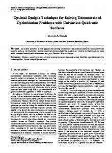
Fig. 3 shows how the error of the computed electron ground state energy in a rectangular quantum well varies with half-width of the solution domain for N = 100 . Both curves shown in this figure exhibit minima around d min = 20 nm. The existence of the minimum is a consequence of the rapid decay of the electron wave function inside the barrier. When the solution domain width increases above d min , the number of the grid points inside the barrier, where the wave function has small magnitude, increases, therefore the error increases. Also, increase of the solution domain leads to reduction of the number of the grid points inside the quantum well where the electrons are mostly localized. It is obvious in Fig. 3 that the FEM produces more accurate result than the FDM for d > d min . We note that the error in Fig. 3 is computed for only several values of d according to equations (17) and (18). Therefore, the oscillations of the error of the electron ground state which are demonstrated in Figs. 1 and 2 are not present in Fig. 3. The deviation of the computed electron ground state from the exact value in the cylindrical nanowire having the rectangular potential as function of the wire radius is shown in Fig. 4. It is evident that ΔE computed by both the FDM and the FEM shows minimum at d min = 20 nm, which is close to the value determined for the planar geometry. However, the error of the calculation by both methods is less sensitive to variation of d when d > d min . This could be explained to be an effect of a faster decay of the wave function in the barrier, and less varying wave function inside the wire. Therefore, the wave functions in quantum wires are well represented by discretization at smaller number of the grid points. We found that the diagrams for the higher energy states have forms similar to Figs. 3 and 4. Also, we found that the variations of ΔE with d have similar 79
D. Topalović, S Pavlović, N. Čukarić, M. Tadić
shapes for the 1D LHO and the isotropic 2D LHO. But, for these latter potentials we also inspected how d min varies with the grid size and the width of the confining potential well, which is proportional to the exact value of the ground state energy E0 . -3
x 10 3.5 FDM FEM 3
ΔEFD1 , Δ EFEM1 [eV]
2.5
2
1.5
1
0.5
0 10
20
30
40
50 60 d [nm]
70
80
90
100
Fig. 3 – The error of the computed ground-state electron energy in the rectangular quantum well as function of the solution domain half-width. The FDM result is shown by the blue line, and the result of the FEM calculations is shown by the green line. -3
8
x 10
FDM FEM
7
Δ EFD1 , Δ EFEM1 [eV]
6 5 4 3 2 1 0 10
20
30
40
50 60 d [nm]
70
80
90
100
Fig. 4 – The error of the computed electron ground-state energy in the cylindrical quantum wire with the rectangular shape of the confining potential as function of the solution domain radius.
80
The Optimal Dimensions of the Domain for Solving the Single-Band Schrödinger…
100
dFEM,min [nm]
80 60 40 20 0 0 0 100 0.5
200 300
1
E0 [eV]
N
Fig. 5 – The optimal half-width of the solution domain as function of the number of elements and the exact energy of the electron ground state in the planar quantum well with the potential of the 1D LHO.
dFEM,min [nm]
150
100
50
0 0 100
0 0.2 0.4
200 0.6 0.8 300 N
1
E0 [eV]
Fig. 6 – Dependence of the optimal radius of the solution domain on the number of the elements and the exact energy of the electron ground state in the axially symmetric quantum wire with the potential of the 2D LHO.
The diagrams determined by means of the FEM are displayed in Figs. 5 and 6 for the planar and cylindrical geometry, respectively. It is obvious that for the 81
D. Topalović, S Pavlović, N. Čukarić, M. Tadić
given width of the quantum well the optimal dimension of the solution domain weakly depends on the number of elements. On the other hand, d min decays fast with E0 in the range from 0 to 100 meV. The functions shown in Figs. 5 and 6 can be fitted with α (19) d min ( E0 , N ) = 0 log αe 1 ( α 2 N ) , E0
where α 0 , α1 , and α 2 are the fitting parameters. The values of the fitting parameters for the potential of the LHO in the quantum well (QW) and the quantum wire (QWR) are shown in Table 1. The difference between the parameters extracted from the calculations by the two numerical methods is found to be small, and the fitting parameters for the quantum wells and quantum wires have the similar values. Table 1 The values of the parameters of the function given by (19) obtained as the best fits of the results shown in Figs. 5 and 6.
α0
α1
α2
0.8365
0.5774
5.187
FEM
1.146
0.4821
3.331
QWR
FDM
1.318
0.4444
4.529
QWR
FEM
1.837
0.4462
6.437
Structure
Method
QW
FDM
QW
[nm(eV)1/2 ]
Finally, we adopt the FEM to numerically compute the energy levels in the quantum well having the shape of the modified Pöschl-Teller potential Vp V0 ( z ) = − . (20) cosh[( V p / c ) z ] In this case the accuracy of the calculations depends on both the width and the depth of the potential well, as Fig. 7 shows. We found that the error of the electron ground energy level determined by the FEM decreases when either the well width decreases (the parameter c of the potential increases) or the well depth (the parameter Vp) increases. The variation shown in Fig. 7 could be explained by better localization of electrons in deeper and wider quantum wells. We also employed the FDM to determine the electron states in the modified Pöschl-Teller potential, and we found it resembles the diagram shown in Fig. 7. 82
The Optimal Dimensions of the Domain for Solving the Single-Band Schrödinger…
16
dFEM,min [nm]
14
12 10
8 3.5 3
0.4 0.35
2.5
0.3
2 c 1/2 [eV1/2nm]
0.25 1.5
0.2
Vp [eV]
Fig. 7 – The optimal dimension of the solution domain as function of the parameters of the modified Pöschl-Teller potential.
5
Conclusion
The finite-difference and finite-element methods are employed to solve the single-band Schrödinger equation in the GaAs/(Al,Ga)As quantum wells and cylindrical quantum wires. We showed that the computation grid should be constructed with care at the abrupt interface between the well and the barrier. For an arbitrary grid the error of the electron ground state energy exhibits oscillations when the number of the grid points varies. We found that the FEM results are more accurate for the given grid size, and that the error of the electron energy levels in the quantum wells and wires computed by the FEM are less dependent on the size of the solution domain than the energy levels determined by the FDM. Furthermore, the optimal value of the dimension (halfwidth or radius) of the solution domain, for which the ground state is computed with the lowest error, is determined. For the potentials of the 1D and 2D linear harmonic oscillators the optimal solution domain width is found to vary negligibly with the number of the grid points, whereas it exhibits strong dependence on the width of the potential well. Moreover, our calculations for the modified Pöschl-Teller potential demonstrate that the accuracy of the electron ground state energy depends on both the well width and depth.
6
Acknowledgment
This work was supported by the Ministry of Education, Science and Technological Development of Republic of Serbia. 83
D. Topalović, S Pavlović, N. Čukarić, M. Tadić
7
References
[1]
J.H. Davies: The Physics of Low-dimensional Semiconductors: An Introduction, Cambridge University Press, Cambridge, UK, 1998. [2] L.R. Ram-Mohan, K.H. Yoo: Wavefunction Engineering of Layered Semiconductors: Theoretical Foundations, Journal of Physics: Condensed Matter, Vol. 18, No. 49, Dec. 2006, pp. R901 – R917. [3] T. Ihn: Semiconductor Nanostructures: Quantum States and Electronic Transport, Oxford University Press, Oxford, UK, 2010. [4] C. Galeriu, L.C.L.Y. Voon, R. Melnik, M. Willatzen: Modeling a Nanowire Superlattice using the Finite Difference Method in Cylindrical Polar Coordinates, Computer Physics Communications, Vol. 181, No. 2, Feb. 2004, pp. 147 – 159. [5] M.E. Pistol, C.E. Pryor: Band Structure of Core-shell Semiconductor Nanowires, Physical Review B: Condensed Matter and Materials Physics, Vol. 78, No. 11, Sept. 2008, p. 115319. [6] C.A. Duarte: Convergence and Instability of Iterative Procedures on the One-dimensional Schrödinger–Poisson Problem, Computer Physics Communications, Vol. 181, No. 9, Sept. 2010, pp. 1501 – 1509. [7] H. Shao, Z. Wang: Arbitrarily Precise Numerical Solutions of the One-dimensional Schrödinger Equation, Computer Physics Communications, Vol. 180, No. 1, Jan. 2009, pp. 1 – 7. [8] L.R. Ram-Mohan: Finite Element and Boundary Element Applications in Quantum Mechanics, Oxford University Press, Oxford, UK, 2002. [9] J.E. Pask, B.M. Klein, C.Y. Fong, P.A. Sterne: Real-space Local Polynomial Basis for Solid-state Electronic-structure Calculations: A Finite-element Approach, Physical Review B: Condensed Matter and Materials Physics, Vol. 59, No. 19, May 1999, pp. 12352 – 12358. [10] J.E. Pask, B.M. Klein, P.A. Sterne, C.Y. Fong: Finite-element Methods in Electronicstructure Theory, Computer Physics Communications, Vol. 135, No. 1, March 2001, pp. 1 – 34. [11] C.A. Duque, M.A. Mora-Ramos: Electron States and Related Optical Responses in Asymmetric Inverse Parabolic Quantum Wells, Superlattices and Microstructures, Vol. 54, Feb. 2013, pp. 61 – 70. [12] Q. Zhongliang, T. Xiaohong, L.E.K. Kenneth, L.P. Huei, B. BaoXue: Large Energy Bandgap Tuning of 980 nm InGaAs/InGaAsP Quantum Well Structure via Quantum Well Intermixing, Solid-State Electronics, Vol. 79, Jan. 2013, pp. 281 – 284.
84