Theoretical Physics Institute, University of Minnesota, Minneapolis, MN 55455. We study the .... and |2ã, corresponding to zero and two electrons occupy-.
Theory of Andreev reflection in a junction with a strongly disordered semiconductor I.L. Aleiner, Penny Clarke, and L.I. Glazman Theoretical Physics Institute, University of Minnesota, Minneapolis, MN 55455 We study the conduction of a N - Sm - S junction, where Sm is a strongly disordered semiconductor. The differential conductance dI/dV of this N - Sm - S structure is predicted to have a sharp peak at V = 0. Unlike the case of a weakly disordered system, this feature persists even in the absence of an additional (Schottky) barrier on the boundary. The zero-bias conductance of such a junction GNS is smaller only by a numerical factor than the conductance in the normal state GN . Implications for experiments on gated heterostructures with superconducting leads are discussed.
arXiv:cond-mat/9601099v1 23 Jan 1996
PACS numbers: 72.20.-i, 74.80.Fp
Since the seminal work of Andreev1 on the theory of electron transport through an ideal interface between a normal (N) metal and a superconductor (S), significant efforts were undertaken to understand the transport in real NS junctions. It was shown2 that a barrier at the N-S interface reduces strongly the conductance of the boundary between a clean normal metal and a superconductor. Later, experiments3 with semiconductor (Sm) – superconductor junctions revealed in the differential conductance GN S (V ) a broad maximum at zero bias. This feature was explained4 as an interference effect due to the scattering off the Schottky barrier and off the imperfections in the semiconductor. Recent technological advances have resulted in fabrication of low-resistance contacts between a two-dimensional electron gas (2DEG) and a superconducting lead5 . Because of the absence of a Schottky barrier at the interface, the subgap conductance is determined by the propagation of electron pairs through the 2DEG itself rather than by two-electron tunneling at the interface, and there is no peak6 in the differential conductance at zero bias. The advantage of a gated heterostructure lies in the controllable level of carrier density in the 2DEG. Depending on the density, the 2DEG may behave as a good conductor or as an insulator with an adjustable localization length. Whereas the former case has been extensively studied both theoretically and experimentally6 , the latter case has received no attention as of yet. In this paper we study two-electron transport through a disordered insulator. We will show that the zero bias conductance of the N - Sm - S junction differs from the conductance of the same structure in the normal state by a numerical factor only. This is similar to the properties exhibited in the metallic regime. However, the differential conductance GN S (V ) drops abruptly with increasing voltage, in contrast to the behavior in the metallic regime in the absence of the Schottky barrier. The development of this feature of the I-V characteristic under the progressive depletion constitutes the signature of the crossover between the metallic and insulating regimes. Deep in the insulating regime, the conductance of the normal (N - Sm - N) structure is dominated by tunneling via those configurations of localized states in the semiconductor layer that facilitate resonant transmission of electrons7 . An example of such a configuration is a state
with energy close to the Fermi level and location symmetric with respect to the leads. The transmission coefficient for an electron tunneling through a resonant configuration is close to unity, and the conductance is proportional to the probability w of finding such a configuration.This probability scales exponentially with the length of the Sm region, L. The zero-bias conductance of the N - Sm - S junction, GN S (0), is determined by the tunneling of pairs of electrons at the Fermi level1 . Clearly, these tunneling processes are also facilitated by the same resonant configurations that control single-electron transport. Thus, the conductance GN S (0) is also proportional to w and, therefore, it has the same exponential dependence upon L as the does normal conductance. If a finite bias eV is applied to the junction, the energies ǫ1 , ǫ2 of the two electrons in the pair are different: ǫ1 − ǫ2 = 2eV . If eV exceeds the width of the resonant level with respect to tunneling, this level cannot provide a large tunneling coefficient for both electrons. It results in a sharp drop of the conductance with voltage. Following Ref. 8, we model transport through the depleted region as resonant tunneling via isolated localized states (impurities). We will show that for a wide range of lengths L, it suffices to consider the single impurity configurations only. In order to calculate the conductance, we first calculate the contribution to the conductance due to tunneling through a single impurity gN S (eV ) and then sum these partial conductances over all the impurities. Each localized state is characterized by its energy (j) ǫj and by the level widths Γl(r) due to the decay into the left (right) lead, see Fig. 1a. The amplitude of electron transmission through the barrier via the resonant state, t(j) (ǫ), and the amplitude of reflection, r(j) (ǫ), at energy ǫ are given by the single channel Breit-Wigner formula: � � (j) (j) ǫ − ǫ j + i Γl − Γr � �, r(j) (ǫ) = (j) (j) ǫ − ǫ j + i Γl + Γr q (j) (j) −2i Γl Γr � �. (1) t(j) (ǫ) = (j) (j) ǫ − ǫ j + i Γl + Γr (j)
The tunneling widths Γl(r) depend exponentially on the
1
distance of the impurity from the middle of the barrier, xj , (see also Fig. 1a): (j)
Γl
−(L−2xj )/a0 , Γ(j) r = E0 e
= E0 e−(L+2xj )/a0 ,
the energy near the Fermi level within the strip of width Γ1 and positioned within the strip of the width a0 around the middle of the barrier, so that Γl ≃ Γr . Therefore, the factor ρa0 W Γ1 is just the number of such states. Result (8) at V = 0 was obtained independently in Ref. 10. Let us estimate the domain of parameters within which the mehanism of tunneling through rare single resonant states dominates over direct tunneling through the potential barrier created by the depleted Sm layer. The contribution of the latter mechanism can be estimated 2 as Gdir h)(kF W )e−2L/a0 , where kF is the Fermi N ∼ (e /¯ wave vector in the N lead. Thus direct tunneling is irrelevant for not too short barriers: � � ma0 kF . (9) L ≫ a0 ln ¯h2 ρ
(2)
where a0 is the localization radius of the impurity state, and the energy E0 can be estimated as E0 ≃ ¯h2 /ma20 , with m being the electron mass in the Sm layer. The Andreev reflection probability can be expressed6 in terms of the one-electron amplitudes t(j) (ǫ) and r(j) (ǫ). The corresponding contribution gN S (eV ; xj , ǫj ) of localized state j to the conductance is: 2 ∗ 2e2 t(j) (eV )t(j) (−eV ) (3) gN S (eV ; xj , ǫj ) = ∗ (−eV ) . π¯ h 1 + r(j) (eV )r(j) (We will restrict our discussion to the most interesting regime of the bias being small compared to the superconducting gap.) Now we sum up the contributions to the conductance from different impurities. Assuming that the density of the localized states ρ is independent of energy, we obtain: (1)
GN S (eV ) = ρW
Z
∞
dǫj −∞
Z
This condition is easily met in the experimental situation7,11 . (1) The linear conductance, GN S (0), differs only by a nu(1) merical factor from GN because the optimal configurations contributing to both quantitites are the same. It changes drastically when the the bias increases, eV ≫ Γ1 . In this regime we obtain from Eq. (4)
L/2
dxj gN S (eV ; xj , ǫj ). (4) (1)
−L/2
Here W is the width of the barrier. The calculation of the conductance is thus reduced to the integration in Eq. (4), with the help of formulas (1) – (3). In the low bias limit, eV ≪ Γ1 , we find " � �2 # Γ(3/4)2 Γ(1/4)2 eV e2 (1) √ √ , (5) + GN S = (ρa0 W Γ1 ) ¯h π 96 π Γ1
(1)
(1)
e2 ρW π¯h
Z
∞
−∞
dǫj
Z
L/2
dxj gN (eV ; xj , ǫj ),
−L/2
gN (eV ; xj , ǫj ) =
e2 |t(j) |2 . π¯ h
(6)
A simple calculation based on (1) and (6) gives8,9 (1)
GN =
e2 (πρa0 W Γ1 ) . h ¯
Comparing Eqs. (5) and (7) we obtain: " � �2 # eV (1) (1) . GN S = GN 0.27 + 0.049 Γ1
Γ1 . eV
(10)
The main contribution to GN S (V ) comes not from the impurities located near the middle of the barrier but rather from ones shifted closer to the S lead. Result (10) can be understood using the following arguments. Consider the impurity lying at the Fermi level, ǫj = 0, that is completely decoupled from the normal lead, Γl = 0. The tunneling of an electron pair between the superconductor and the impurity mixes the states |0i and |2i, corresponding to zero and two electrons occupying the impurity. As the result, the four-fold degeneracy of the impurity level is partially lifted: two singly occupied states still have energy ǫj = 0, but the other two states, |0i − |2i and |0i + |2i, are split by 2Γr symmetrically with respect to the Fermi level. The even wave function is the ground state of the impurity, and the smallest excitation energy (to the singly occupied state) is Γr . Let us now turn on a small coupling between the impurity and the normal lead, Γl ≪ Γr . This coupling enables the electron to tunnel from the Fermi level in N lead to the impurity level. This tunneling is resonant if the potential drop on the contact eV is close to the energy of excitation, |eV − Γr | < ∼ Γl . A similar consideration is valid for all the impurities with energies |ǫj | < ∼ Γr . Now, we find the impurities that give the maximal contribution to the conductance. The transmission coefficient is close to unity for the impurities with Γr = eV , i.e. at eV > Γ1 the optimal impurities are shifted towards the superconducting lead. The energies of these impurities may lie in the strip of the width Γr about the Fermi level. The coordinate xj of the impurity may deviate from its optimal
where Γ1 ≡ E0 e−L/a0 is the level width of a state localized at xj = 0, and Γ(x) is the Gamma function. It is instructive to express this result in terms of the normal state conductance of the same junction: GN =
(1)
GN S (V ) = GN
(7)
(8)
Results (5) and (7) can be easily understood. The contribution of the single-site resonant states to both GN and GN S is determined by the number of the states with 2
value by no more than ±a0 Γl /Γr , as it follows from the condition |eV − Γr | < ∼ Γl , and Eq. (2). This consideration shows that the number of relevant impurities is of the order of ρa0 Γl Γr /eV , which with the help of Eqs. (2) and (7) immediately yields Eq. (10). As the barrier length is increased, the dominant mechanism of electron transport shifts from the single-state configurations to the configurations containing “chains” of two localized states8 . These configurations are more complex than the ones considered before, nevertheless Eq. (3) is still valid. The only difference is that the one electron reflection and transmission amplitudes now depend upon the energies ǫjl , ǫjr and positions r jl , rjr of the two impurities, see Fig. 1b. Each impurity is characterized by its coupling to the nearest lead, see Fig. 1b, Γ(jl ) = E0 e−(L+2xjl )/a0 ,
Similar to the case of single impurity configurations, it is convenient to express the result in terms of the contribution of two-impurity chains to the normal conductance. (2) This contribution GN , is given by8 (2) GN (eV
dǫjr dǫjl dyjl
Z
L/2
dxjr −L/2
Z
xjr
dxjl
−L/2
(15)
where the partial conductances gN are obtained from Eqs. (6) and (1) by the substitution of (14a) and (14b). Simple integration in Eq. (15) yields r π 2 (1) (2) ρL E1 GN , (16) GN = 3 2 (1)
where GN is the single impurity result Eq. (7). Twoimpurity chains dominate the conductance8,9 if the disordered region is long enough: L> ∼ a0
where the energy E1 is of the order of E0 . After one finds the partial conductance gN S of a single (2) two-impurity “chain”, the net contribution GN S (eV ) of these chains to the total conductance can be calculated in a manner similar to that used previously for the singleimpurity configurations: ZZZ ∞ Z xjr Z L/2 (2) dxjl dǫjr dǫjl dyjl GN S (eV ) = ρ2 W dxjr ×gN S (eV ; ǫjr , ǫjl , xjl , xjr , yjl − yjr ).
∞
×gN (eV ; ǫjr , ǫjl , xjl , xjr , yjl − yjr ),
Γ(jr ) = E0 e−(L−2xjr )/a0 . (11)
−L/2
)=ρ W
ZZZ
−∞
The coupling between the two impurities is given by �1/2 � a0 e−|rjl −rjr |/a0 , (12) hjl jr = E1 |r jl − r jr |
−∞
2
�
m ¯h2 ρ
�1/2
.
(17)
(We used here the estimate E1 ∼ E0 ∼ ¯h2 /ma20 .) Deep in the insulating regime, where the separate impurity states overlap weakly, the parameter h ¯ 2 ρ/m is small, and the condition (17) is more restrictive than (9). If the length of the barrier increases further, more complex configurations may contribute. The effects associated with these configurations have not been observed experimentally for the normal conductance and we will not consider their contributiton to GN S . Now we present our results for the two-impurity contribution to N - Sm - S conductance obtained by performing the integration in Eq. (13). At zero-bias, we found
−L/2
(13)
The formulas for the reflection and transmission amplitudes entering gN S for an arbitrary impurity pair are quite cumbersome. Fortunately, the dominant part of the average (13) comes from the impurity pairs with sufficiently large energy difference, |ǫjl − ǫjr | ≫ hjl jr . This means that one of the two impurities serves as a resonant level for the incoming electron, while the second impurity provides a virtual state which modifies the escape rate from the resonant level into the lead. Therefore, for the relevant “chains” the reflection and transmission amplitudes are given by Eq. (1) with the level widths renormalized by the tunneling through a virtual state. Depending on which component of the pair is in resonance, we find: � �2 hjl jr (j) (jr ) ǫj → ǫjl , Γl → Γ(jl ) , Γ(j) → Γ (14a) r ǫjl − ǫjr
(2)
GN S (0) =
Γ(3/4)2 (2) (2) √ GN ≈ 0.27GN . π
(18)
It is important to emphasize that the relationships between the contributions to the N - Sm - S and N - Sm N conductances are identical for one- and two-impurity configurations, see Eq. (8). This is because within the optimal two-impurity chains only one level is in resonance, and the other level is responsible only for the tunneling width. The same argument also apply for the one dimensional chains consisting of a larger number of impurities. Therefore, we believe, that the relation GN S (0) = 0.27GN is a universal property of disordered junctions for which the conductivity occurs via the tunneling through quasi-one-dimensional chains containing an arbitrary number of impurities. (2) For a finite bias, however, the relationship beween GN S (2) and GN is quite different from Eq. (10): the differential (2) conductance GN drops only logarithmically with the increase of V . The strongest variation of the conductance,
if the left impurity is in resonance, or � �2 hjl jr (j) ǫj → ǫjr , Γl → Γ(jl ) , Γr(j) → Γ(jr ) (14b) ǫjl − ǫjr if the right impurity is the resonant one. The corresponding contributions to gN S are obtained from Eqs. (3) and (1) by the substitutions (14a) and (14b) respectively. 3
(2)
(2)
GN S (eV ) = GN S (0)
4a20 2 ln 3L2
�
Γ2 eV
�
,
1
A.F. Andreev, Zh. Exp. Teor. Fiz. 46, 1823 (1964) (Sov. Phys. JETP, 19, 1228 (1964)). 2 G. E. Blonder, M. Tinkham, and T. M. Klapwijk, Phys. Rev. B. 25, 4515 (1982). 3 A. Kastalsky et. al., Phys. Rev. Lett. 67, 3026 (1991). 4 B.J. van Wees et. al., Phys. Rev. Lett. 69, 510 (1992); F.W.J. Hekking and Yu.N. Nazarov, Phys. Rev. Lett. 71, 1625 (1993); Phys. Rev. B 49 6847 (1994). 5 B.J. van Wees et. al., Physica B 203, 285 (1994); H. Kroemer et. al., ibid. 299. 6 For review see, e. g., C.W.J. Beenakker in Mesoscopic Quantum Physics, E. Akkermans, G. Montambaux, and J.L. Pichard, eds., North Holland, Amsterdam, (to be published); T.M. Klapwijk, Physica B 197, 481 (1994). 7 M. Naito and M.R. Beasley, Phys. Rev. B 35, 2548, (1987) 8 A.I. Larkin and K A. Matveev, Zh. Exp. Teor. Fiz.93, 1030 (1987) (Sov. Phys. JETP, 66, 580 (1987)). 9 The difference between our expressions for the normal conductance and those from Ref. 8 is due to the 2D depleted layer in our case, whereas 3D amorphous barier was considered in Ref. 8. 10 A.V. Dyomin, V.A. Khlus, and L.P. Chernyakova, Fiz. Niz. Temp. 21, 531 (1995) (to appear in: Low Temp. Phys.) 11 D. Popovic, S. Washburn, A. B. Fowler, Int. J. Mod. Phys. B,8 809 (1994)
(19)
< occurs in the region Γ1 < ∼ eV ∼ Γ2 . Here Γ2 ≡ E0 exp(−L/2a0 ) = Γ1 exp(L/2a0 ) is the characteristic width of a resonant level formed by a two-impurity chain. The reason for the logarithmic dependence (19) is the following. As we already discussed, the transmission coefficient for two electron tunneling through the localized level is close to unity, if two conditions are met: (i) the tunneling rates Γl , Γr are approximately the same, and (ii) the difference between the energies of the two tunneling electrons is less than the level width, eV < Γl,r . For the single impurity configuration, the first condition can be met only for the impurities located in the vicinity of the middle of the barrier, therefore, the sharp drop occurs at eV ∼ Γ1 . However, for the two impurity configuration, the first condition can be satisfied for various configurations {xjl , xjr }. The largest level width compatible with the condition (i), Γ2 = Γ1 eL/2a0 , corresponds to the largest separation X = L/2 between the two impurities. On the other hand, condition (ii) restricts the separation from below, X > ∼ a0 ln(eV /Γ1 ), which eventually leads to Eq. (19). Comparison of Eq. (10) with Eq. (19) shows, that even if at low biases conductance is dominated by single-impurity channels, a crossover to the two impurities“chain” configurations may occur at larger eV . This crossover from a sharp function (10) to a much slower logarithmic dependence (19) takes place at voltage � � e−λ L m eV ∗ ≃ 2 Γ2 , λ ≡ . − ln λ 2a0 h2 ρ ¯
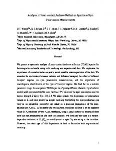
FIG. 1. Schematic picture of the N - Sm - S junction with (a) single localized state, (b) two-impurity chains
FIG. 2. Voltage dependence of the differential N - Sm - S conductance contributed by single impurity configurations, (1) GNS (V ).
At this bias, the optimal configurations changes from single impurity to two impurities “chains”. To observe the crossover, the junction parameters should satisfy the condition: � �1/2 m 1≪λ≪ . h2 ρ ¯ In conclusion, we studied the conductance of the N Sm - S junction where Sm is a strongly disordered semiconductor. The electron transport is due to resonant tunneling through the levels localized in Sm. We find, that at zero-bias N - Sm - S conductance is proportional to the conductance of the same junction in the normal state, GN S (0) = 0.27GN . At larger biases, the conductance GN S (V ) drops drastically. This drop represents the signature of Andreev reflection in a junction with a strongly disordered semiconductor. Discussions with F.W.J. Hekking are acknowledged with gratitude. This work was partially supported by the Minnesota Supercomputer Institute and by NSF Grant DMR-9423244.
4
ε
Fig. 1
(a)
N
Sm
S
εj
x
-L
xj
2
L 2
ε
(b)
N
Sm ε jr
S
εj
x
l
-L
2
xj
l
xjr
L 2
Fig. 2 GNS GN 0.3
0.2
0.1
eV Γ - 6
- 4
- 2
0
2
4
6