The focus of this work is about the nanostructure of sputtered TiN-TiB2 films, .... the reduction of the B-content is preferably on the expanse of the disordered ...
Mater. Res. Soc. Symp. Proc. Vol. 854E © 2005 Materials Research Society
U6.2.1
Thermal Stability of Nanostructured TiN-TiB2 Thin Films Paul H. Mayrhofer and Christian Mitterer Department of Physical Metallurgy and Materials Testing, University of Leoben, A-8700 Leoben, Austria ABSTRACT Nanocrystalline hard films have attracted increasing interest for wear-resistant applications. Especially, films within the system Ti-B-N with its numerous different phases are ideal candidates for materials science based studies on the nanoscale. In physical vapor deposited TiB-N films the nanostructure arises during growth by segregation-driven renucleation resulting in 2-3 nm sized TiN and TiB2 crystals. These films exhibit a hardness of ~ 42 GPa in the asdeposited state which increases to ~ 52 GPa during thermal annealing in vacuum. Here we show, that as-deposited films have a remarkable fraction of disordered regions surrounding TiN and TiB2 nanocrystals. During thermal annealing, the structural rearrangement causes the formation of compact boundary areas, leading to a hardness increase. At temperatures higher than 900 °C, the occurring B-loss, grain-growth, and recrystallization cause the hardness to decrease. INTRODUCTION Thin transition metal nitride, boride and carbide films are the topic of many papers due to their physical, chemical and mechanical properties which make them applicable for several industrial fields [1-12]. Among these, boron containing thin films have attracted increasing interest due to their outstanding hardness and thermal stability [1-9,13-16]. The increasing industrial demand for advanced protective thin films with tailored properties requires the development of multi-elemental and multi-phase ceramic layers. In particular, films within the system Ti-B-N with its numerous different phases are challenging candidates for materials science based studies [2,5], also due to their possible nanocrystalline structure. The latter results from a segregationdriven renucleation process during growth of the multiple phases present [13,14]. The focus of this work is about the nanostructure of sputtered TiN-TiB2 films, its modification during annealing treatments up to 1400 °C and the effects of the nanostructural arrangement on the film hardness. Here we show, using x-ray diffraction and high resolution transmission electron microscopy, that sputtered TiN-TiB2 films are composed of randomly orientated 2-3 nm sized TiN and TiB2 crystals surrounded by a B-rich disordered region. During post-deposition annealing treatments in vacuum, the nanostructural arrangement modifies itself, causing a hardness increase starting from ~ 42 GPa in the as-deposited state to ~ 52 GPa after annealing at 900 °C. Annealing at higher temperatures causes B-loss [16], grain growth and recrystallization [17] of the film, resulting in a hardness decrease. The results for TiN-TiB2 films show a clear correlation between their nanostructure, modified by annealing, and their mechanical properties. EXPERIMENTAL TiN-TiB2 films [13], ~ 3 µm thick, were grown on polished austenitic stainless steel substrates at 300 °C by magnetically-unbalanced magnetron sputter deposition from a segmented
U6.2.2
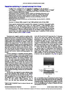
sintered TiN-TiB2 target (both segments of 99.5 % purity and with a shape of a half-disc, 150 mm in diameter) in Ar (99.999 % purity) discharges [15]. The Ar pressure and magnetron power density are 0.4 Pa (53.3 Torr) and 3.5 W·cm-2, respectively, yielding a deposition rate R of 0.56 nm·s-1. The deposition system and growth conditions are described in more detail in refs. [15,18]. The incident metal flux JTi was estimated based upon measured R values, film composition, film thickness, and assuming bulk density. The ion flux JAr+ and the ion energy EAr+ bombarding the growing film are determined using Langmuir-probe measurements following the procedures described in ref. [19]. The incident ion/metal flux ratio JAr+/JTi and EAr+ are 3.3 and 30 eV, respectively, during growth. Deposited films on stainless steel substrates are annealed in vacuum at temperatures Ta up to 1100 °C at pressures ≤ 10-3 Pa (0.133 Torr) for 30 minutes (heating rate > 100 K·min-1). An additional heat treatment of a film, chemically removed from its polished lowalloyed steel substrate, is carried out in a flow of Ar (99.999 % purity and 50 sccm with atmospheric pressure) at 1400 °C (heating rate = 50 K·min-1). The film chemical composition is determined by wavelength dispersive electron-probe microanalysis using a MICROSPEC WDX-3PC analyzer. Quantification is obtained by means of TiN and TiB2 film standards, calibrated using nuclear reaction analysis. Film hardness H is obtained by computer controlled measurements using a Fischerscope H100C with 50 mN load for which the Vickers indentation depth is ≤ 10 % of the film thickness. Structure and morphology of the films are studied by Bragg-Brentano x-ray diffraction (XRD, Siemens D 500) with Cu Kα radiation and transmission electron microscopy (TEM, JEOL 2010F). In addition to highresolution TEM (HRTEM) investigations [13] the crystallite size of the films is estimated from single line profile analyses of XRD patterns fitted with Cauchy functions [20] with peak maxima at TiN and TiB2 diffraction positions, as the film is composed of nearly defect-free TiN and TiB2 nanocrystals [13]. RESULTS AND DISCUSSION The bright field cross-sectional HRTEM (HRXTEM) micrograph in figure 1a shows randomly oriented 2-3 nm sized crystals of the layer in the as-deposited state. The mass (Z) contrast
Figure 1. (a) Bright field HRXTEM image, (b) Z-contrast image indicating at least two different phases, (c) SAED pattern with fcc-TiN and hcp-TiB2 standard diffraction rings.
U6.2.3
image (figure 1b) clearly indicates also a random distribution over the whole film of at least two different phases. It is shown in ref. [13] that although the chemical composition of the film with Ti = 38 at%, B = 30.5 at% and N = 31.5 at% is located in the TiN-TiB2-BN ternary phase field of the equilibrium Ti-B-N phase diagram, the film only consists of stoichiometric TiN and TiB2 crystals encapsulated by B-rich disordered regions. There is no evidence for crystalline BN. The diffraction rings in figure 1c indicate a mixture of TiN and TiB2 nanocrystals with random orientation and a considerable amount of disordered regions. Considering the extremely short diffusion path for point and line defects in 2-3 nm grains to the nearest sink (i.e., grain and phase boundaries, interfaces), almost perfect crystals should form during deposition. Therefore, the film mainly consists of TiB2 and TiN crystals with low defect density [13]. In such nanocomposites with an average grain size of about 2-3 nm the volume fraction of disordered grain and phase boundaries is in the range of ~ 70 % [21]. In Ti-B-N films also the formation of amorphous BN surrounding the nanocrystals is likely [7,16]. However, these disordered boundary regions and the small grain size of 2-3 nm are responsible for an increased interfacial volume fraction explaining the contribution of amorphous-like diffraction rings to the SAED pattern (see figure 1c). The structural evolution with annealing at different temperatures Ta of the TiN-TiB2 film is shown in figure 2 represented by XRD patterns. The steel substrate reflections are at 43.62° and 74.70° [22]. In the as-deposited state the broad film XRD peaks are the result of overlapped broad TiN and TiB2 reflections. Such broad reflections indicate small grain sizes and/or high lattice strains of a crystalline phase but also a huge amount of disordered regions [20]. This is in agreement with HRXTEM and SAED investigations (figures 1a and c) of the TiN-TiB2 film in the as-deposited state. Likewise, also from XRD investigations no evidence for crystalline BN can be found. The high hardness value of ~ 42 GPa for as-deposited films emphasizes also the absence of hexagonal BN. After annealing, the two phases TiN and TiB2 become more pronounced, indicated by their separated XRD peaks for Ta ≥ 800 °C. This indicates an occurring crystal growth, which consequently reduces the disordered boundary fraction (i.e., interfacial fraction), due to increased diffusivity at higher temperatures. A fully recrystallized structure,
(222) (201)
(200) (311)
(102) (111)
(110) (220)
(002)
(200) (101)
TiB2
intensity (arbitrary units)
(100) (111)
TiN;
Ta (°C) 1400 1000 900 800 600 as-dep. 30
35
40
45
60 65 2θ (deg)
70
75
Figure 2. XRD evolution with annealing temperature Ta.
80
U6.2.4
containing just TiN and TiB2 phases, can be seen for Ta = 1400 °C. Corresponding to the nanostructural changes within the film during annealing also the hardness H and the reduced elastic modulus E* (E* = E·(1-ν2)-1, where E is the elastic modulus and ν is the Poisson ratio) change with Ta (figure 3a). An increase of H from ~ 42 to ~ 52 GPa is achieved by an annealing treatment up to 800 °C. If Ta exceeds 900 °C the hardness of the film decreases again, but a hardness value of ~ 42 GPa after annealing at 1000 °C is still extraordinary high for thin films [11,12]. E* slightly increases from ~ 352 GPa in the as-deposited state to ~ 405 GPa after annealing at Ta ≥ 900 °C (see figure 3a). As the hardness increase is more pronounced than the elastic modulus increase, the H/E* ratio [23] increases (figure 3a) from ~ 0.118 (as-deposited) to ~ 0.130 (Ta = 800 °C). This indicates that the H/E* ratio can be optimized by a well designed nanostructural arrangement. As the hardness decreases for Ta ≥ 900 °C and E* remains almost at ~ 408 GPa also the H/E* ratio decreases and is below 0.1 as the grain sizes are above 5 nm [13]. The boron content of the TiN-TiB2 film decreases if Ta ≥ 900 °C, causing a reduction of the B/Ti at%-ratio (see figure 3b), whereas the N/Ti at%-ratio remains constant at ~ 0.83 with Ta ≤ 1100 °C. During annealing at 1100 °C the B/Ti at%-ratio changes from 0.80 to ~ 0.35. This loss of B during annealing at Ta ≥ 900 °C for TiN-TiB2 thin films [13] on stainless steel is attributed to the formation of volatile B-oxides with residual oxygen of the annealing atmosphere [16]. Due to the reduction of the boron content, the TiN-TiB2 film meets the quasi-binary TiN-TiB2 tie line of the Ti-B-N equilibrium phase diagram after annealing at Ta = 1100 °C. Consequently, as the film is composed of the equilibrium phases TiN and TiB2 already in the as-deposited state, the reduction of the B-content is preferably on the expanse of the disordered boundary region [13]. The results of the structural investigations indicate that B-rich boundary regions inhibit grain growth and recrystallization. As a consequence, the effectiveness in hindering grain growth and recrystallization decreases with the B content [15]. Thus, for the TiN-TiB2 film clearly separated TiN and TiB2 XRD peaks can be seen for Ta ≥ 1000 °C, due to the increased crystallite size (figure 3b) which results in a hardness decrease (figure 3a). The average grain size d of TiN and TiB2 crystals, estimated from XRD single line profile analyses, fit very well the HRTEM investigations presented in ref. [13].
45
0.14
40
0.12
35
0.10
30 25
600
800 1000 Ta (°C)
1200
1400
tf (µm)
0.16 H/E* ratio
E*(.10-1), H (GPa)
50
0.18
20
1.0
2.8
18
0.9
2.6
16
2.4
14
2.2
12
2.0
10 tf B/Ti at%-ratio d
1.8 1.6
8 6
0.8 0.7 0.6 0.5 0.4
1.4
4
1.2
2
0.3
0
0.2
1.0
25
600
800 1000 Ta (°C)
1200
1400
Figure 3. (a) Hardness H, reduced elastic modulus E* (E* = E·(1-ν2)-1 and H/E* ratio, (b) film-thickness tf, B/Ti at%-ratio and average grain size d of TiN-TiB2 as a function of Ta.
B/Ti at%-ratio
H E* H/E*
(b) 3.0
d (nm)
(a)
U6.2.5
Since no additional phases are formed during the annealing treatments (see figure 2) [13], the increased hardness for Ta ≤ 900 °C is related to the nanostructural rearrangement and the formation of compact boundary regions due to increased diffusivity. Therefore, also the reduced elastic modulus increases slightly [24]. The formation of compact boundary regions and reduction of their volume fraction, while maintaining a small grain size of ~ 2.7 nm, is fostered by film-thickness tf measurements after annealing at Ta ≤ 1000 °C (see figure 3b). The tf values, obtained from cross-sectional TEM investigations where one deposited sample is cut into pieces which are then individually annealed at Ta, decrease from 2.83 µm (as-deposited) to 2.51 µm (Ta = 1000 °C) indicating that the annealing gives rise to compact boundary regions and reduction of their volume fraction. The observed chemical and structural modifications are additionally corroborated by dynamical differential scanning calorimetric measurements presented in refs. [13,14]. There, especially the exothermic reactions due to B-loss with a peak temperature at ~ 900 °C and pronounced grain growth with a peak temperature at ~ 1100 °C can be detected. These temperatures fit very well the chemical and structural modifications of TiN-TiB2 (see figure 3b). CONCLUSIONS TiN-TiB2 films which were non-reactively co-sputtered from a segmented ceramic TiNTiB2 target in a pure Ar-discharge show the ability to increase their hardness upon annealing in vacuum. Due to a segregation-driven renucleation process during growth, the films are composed of 2-3 nm sized TiN and TiB2 crystals, which are bounded by a B-rich disordered region in the as-deposited state. Although the chemical composition of the films is within the TiN-TiB2-BN ternary phase field of the Ti-B-N phase diagram, no evidence for crystalline BN is found. The HRXTEM, SAED and XRD investigations indicate that excess B, which is preferably located at boundaries, is also responsible for an increased disordered volume-fraction surrounding the TiN and TiB2 nanocrystals. Due to the small crystallite size, where dislocations are unlikely to appear, and the high cohesive strength of the B-rich boundaries, the TiN-TiB2 films exhibit a very high hardness of 42 GPa in the as-deposited state. Post-deposition annealing of the layers gives rise to compact the boundary regions and hence grain boundary sliding is more difficult. Thus, for the film with identical chemical and phase composition and grain size, a pronounced increase of the hardness from ~ 42 to ~ 52 GPa can be obtained after annealing at Ta = 800 °C. The B/Ti at%-ratio of the film decreases during annealing with Ta ≥ 900 °C from B/Ti ~ 0.80 in the as-deposited state to ~ 0.35 for Ta = 1100 °C, whereas the N/Ti at%-ratio remains constant at ~ 0.83 with Ta ≤ 1100 °C. The loss in B, due to the formation of volatile B-oxides, is preferably at the expense of the disordered boundary fraction which inhibits grain growth and recrystallization. As soon as the B content decreases, the film starts to recrystallize and this subsequently results in an increase of the average crystallite size. Accompanied with these processes also the hardness decreases if Ta exceeds 900 °C. The chemical composition of the films after annealing at 1100 °C is situated at the quasibinary TiN-TiB2 tie-line of the equilibrium Ti-B-N phase diagram. Therefore, after annealing at Ta = 1400 °C where the films show a fully recrystallized structure, only TiN and TiB2 phases are present. The results obtained show that properties of hard thin films can be designed by their nanostructure and especially by the interfaces separating the nanocrystals. Thus, such films have a high potential to achieve superior properties which can even improve during high-temperature applications due to diffusion-driven nanostructural rearrangements.
U6.2.6
ACKNOWLEDGEMENT We acknowledge the use of the Center for Microanalysis of Materials, University of Illinois, which is partially supported by the U.S. Department of Energy. REFERENCES 1. 2. 3. 4. 5. 6. 7. 8. 9. 10. 11. 12. 13. 14. 15. 16. 17. 18. 19. 20. 21. 22. 23. 24.
W. Herr, B. Matthes, E. Broszeit, and K.H. Kloos, Mater. Sci. Engin. A 140, 626 (1991). W. Gissler, Surf. Coat. Technol. 68-69, 556 (1994). M. Stoiber, S. Perlot, C. Mitterer, M. Beschliesser, C. Lugmair, and R. Kullmer, Surf. Coat. Technol. 177-178, 348 (2004). P.H. Mayrhofer, C. Mitterer, J.G. Wen, J.E. Greene, and I. Petrov, Appl. Phys. Lett., submitted (2004). T.P. Mollart, M. Baker, J. Haupt, A. Steiner, P. Hammer, and W. Gissler, Surf. Coat. Technol. 74-75, 491 (1995). P. Losbichler and C. Mitterer, Surf. Coat. Technol. 97, 567 (1997). P. Karvánková, M.G.J. Vepřek-Heijman, M.F. Zawrah, and S. Vepřek, Thin Solid Films 467, 133 (2004). C. Mitterer, M. Rauter, and P. Rödhammer, Surf. Coat. Technol. 41, 351 (1990). R. Wiedemann, V. Weihnacht, and H. Oettel, Surf. Coat. Technol. 116-119, 302 (1999). S. Vepřek and S. Reiprich, Thin Solid Films 268, 64 (1995). P.H. Mayrhofer, A. Hörling, L. Karlsson, J. Sjölén, T. Larsson, C. Mitterer, and L. Hultman, Appl. Phys. Lett. 83(10), 2049 (2003). L. Hultman, Vacuum 57, 1 (2000). P.H. Mayrhofer, C. Mitterer, J.G. Wen, I. Petrov, and J.E. Greene, Acta Mat., to be submitted (2005). P.H. Mayrhofer in Nato Science Series II. Mathematics Physics and Chemsitry, edited by A.A Voevodin et al., (Kluwer 155, Amsterdam, 2004) pp. 57-68. P.H. Mayrhofer, H. Willmann, and C. Mitterer, Thin Solid Films 440, 174 (2003). P. Karvánková, M.G.J. Vepřek-Heijman, O. Zindulky, A. Bergmaier, and S. Vepřek, Surf. Coat. Technol. 163-164, 149 (2003). F.J. Humphreys and M. Hatherly (eds.), Recrystallization and Related Annealing Phenomena, (Elsevier, Oxford, 1995). P. Losbichler and C. Mitterer, Surf. Coat. Technol. 97, 567 (1997). I. Petrov, V. Orlinov, I. Ivanov, and J. Kourtev, Contrib. Plasma Phys. 28, 2 (1988). E.J. Mittemeijer and P. Scardi (eds.), Diffraction Analysis of the Microstructure of Materials, (Springer, Berlin, 2004). C. Suryanarayana, Int. Mat. Rev. 40(2), 41 (1995). Powder Diffraction File (Card 33-397), JCPDS-International Center for Diffraction Data, (Swarthmore, PA, 2001). G.M. Pharr, Mater. Sci. Eng. A 253(1–2), 151 (1998). J. Schiøtz, T. Vegge, F.D. Di Tolla, and K.W. Jacobsen, Phys. Rev. B 60(17), 11971 (1999).