APPLIED PHYSICS LETTERS 91, 014101 共2007兲
Threading dislocation behavior in AlN nucleation layers for GaN growth on 4H-SiC Y. N. Picard,a兲 M. E. Twigg, M. A. Mastro, C. R. Eddy, Jr., R. L. Henry, and R. T. Holm Electronics Science and Technology Division, Naval Research Laboratory, Washington, DC 20375
P. G. Neudeck NASA Glenn Research Center, Cleveland, Ohio 44135
A. J. Trunek OAI, Cleveland, Ohio 44135
J. A. Powell Sest, Inc., Cleveland, Ohio 44135
共Received 2 June 2007; accepted 12 June 2007; published online 5 July 2007兲 Threading dislocations in thin 共⬍200 nm兲 AlN nucleation layers 共NLs兲 grown by metal-organic chemical vapor deposition on top of 4H-SiC on-axis mesas with atomic-scale steps were analyzed by transmission electron microscopy. The AlN NL controlled threading dislocations in an overlying ⬃2 m GaN layer through two identified mechanisms: threading half-loop formation and dislocation bending at V-shaped pits. Threading dislocations in the AlN film could be traced directly to bilayer 4H-SiC steps at the substrate/film interface. These observations reveal several approaches to extended defect reduction in GaN films grown on 4H-SiC. © 2007 American Institute of Physics. 关DOI: 10.1063/1.2754638兴 The most viable substrates currently utilized for heteroepitaxial GaN thin film based devices are SiC and sapphire.1 Growing high quality GaN films by metal-organic chemical vapor deposition 共MOCVD兲 has long necessitated the use of a nucleation layer 共NL兲.2 AlN NLs continue to be utilized for alleviating strain due to the large lattice mismatch between GaN and sapphire 共16%兲 or SiC 共3.5%兲. Nevertheless, threading dislocation densities in MOCVD GaN commonly reach 108 – 1010 / cm2 and degrade optoelectronic device properties, such as UV electroluminescence.3 Strategies in addition to NL optimization have been investigated to reduce the threading dislocation density in III-nitride films. These methods include control of NL growth,4,5 higherpressure GaN growth,6,7 and lateral epitaxial overgrowth.8 A different approach to reducing extended defects in MOCVD III-nitride films involves improving the morphology of the substrate surface.9,10 By following patterned reactive ion etch delineation of SiC substrates with hightemperature, step-flow SiC homoepitaxial growth, it is possible to create 50– 200 m wide 4H-SiC mesa surfaces with significantly reduced surface step densities. For the case where no substrate screw dislocations penetrate the mesa, atomically flat and step-free 4H-SiC surfaces are achievable.11,12 Atomic steps on SiC substrate surfaces have been linked to the nucleation of threading dislocations in III-nitride films grown on SiC substrates.13 In this work, we utilize stepped 4H-SiC mesa structures 共i.e., SiC mesas topped with screw-dislocation growth steps兲 to investigate the threading dislocation behavior in AlN nucleation layers grown on 4H-SiC and the resulting influence those defects have on extended defects in overlying GaN films. It is useful to note that such stepped surfaces closely resemble conventional, full-wafer SiC surfaces. Following 4H-SiC on-axis mesa preparation,11,12 an ⬃100 nm AlN nucleation layer and a兲
Electronic mail:
[email protected]
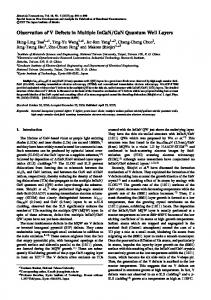
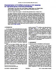
an ⬃2 m GaN film were deposited in a MOCVD reactor; details of which are reported elsewhere.14 Final structures were cross sectioned with a FEI Nova Nanolab focused ion beam system and analyzed by transmission electron microscopy using a Hitachi H-9000UHR operating at 300 keV. Patterned mesa surfaces initially penetrated by screw dislocations prior to two-dimensional SiC growth will continue to contain steps with two 共0.5 nm兲, four 共1.0 nm兲, or greater bilayer step heights.12,13 Lattice imaging along the ¯¯10兴 zone axis reveals the presence of such multibilayer 关21 height steps at the AlN / SiC interface. These steps are shown to be directly responsible for the creation of threading dislocations at the AlN / SiC interface, such as the example shown in Fig. 1. The sample in Fig. 1 was ion milled until sufficiently thin that the 共0002兲 lattice fringes could be resolved but still thick enough to contain the mixed threading dislocation emanating from the step with sufficient contrast. This observation illustrates how reducing the density of bilayer steps on the surface of the SiC substrate results in a lower threading dislocation density in the AlN NL.10,11 Figure 2 shows a bright field cross-section transmission electron microscopy 共TEM兲 image of screw-component threading dislocations in the AlN NL. The AlN film exhibits a large degree of strain contrast near the SiC interface due to high concentrations of defects. The threading dislocations begin at the AlN / SiC interface and progress toward the film surface but not all necessarily reach the GaN / AlN interface. Bright field imaging using two-beam conditions indicated that threading dislocations in the AlN NL were composed of nearly equal parts edge and screw components. Many isolated threading half-loops 共an example denoted by a black arrow in Fig. 2兲 were observed in the AlN nucleation layer and have two possible formation mechanisms. One possible explanation for the presence of half-loops is that pairs of threading dislocations with opposite Burgers vector are combining. Such an annihilation mechanism has
0003-6951/2007/91共1兲/014101/3/$23.00 91, 014101-1 © 2007 American Institute of Physics Downloaded 17 Apr 2008 to 132.250.135.192. Redistribution subject to AIP license or copyright; see http://apl.aip.org/apl/copyright.jsp
014101-2
Picard et al.
Appl. Phys. Lett. 91, 014101 共2007兲
FIG. 1. Cross-section TEM images of 共a兲 the AlN / SiC interface recorded ¯¯10兴 zone axis at an isolated screw-component threading disloalong the 关21 cation and 共b兲 a higher magnification lattice image showing the presence of a two bilayer, 0.5 nm high 4H-SiC step as the source of the AlN threading dislocation.
been recently reported for AlN films grown by molecular beam epitaxy on sapphire15 and sublimation epitaxy on SiC.16 Another possibility is that half-loops form during the initial stages of nucleation and growth of the AlN film. The presence of isolated threading half-loops has not been previously reported in thin 共⬍200 nm兲 AlN films,17 and this phenomenon might suggest that these defects may initially nucleate as half-loops rather than growing as individual threading dislocations that mutually annihilate adjacent threading dislocations as the AlN film is grown to greater thicknesses. Threading dislocation densities in the AlN nucleation layer near the GaN / AlN interface are estimated to be ⬃1011 / cm2. When threading dislocations do reach the AlN film surface, many continue into the overlying GaN film. Weakbeam dark field cross-sectional imaging indicated that the threading dislocations had greater edge than screw components in the GaN film. Total threading dislocation densities were estimated to reach 1010 / cm2 in the GaN film ⬍500 nm from the GaN / AlN interface. Figure 3 shows individual screw/mixed type threading dislocations, denoted by white
¯¯10兴 zone axis FIG. 3. Bright field TEM images of the AlN layer near the 关21 and g = 0002 with 共a兲 pairs of screw/mixed threading dislocations identified in the GaN and labeled A and B and a V-shaped pit at the AlN / GaN interface labeled V; a higher magnification TEM image 共b兲 is included showing the V-shaped pit and the B threading dislocations forming a half-loop in the GaN film.
arrows and labeled A or B, continuing from the AlN film and into the GaN film. Upon penetrating the GaN film, the A threading dislocations continue upward to the GaN film surface while the pair of B threading dislocation combine to form a dislocation half-loop 关Fig. 2共b兲兴. Bright field and dark ¯0 field imagings of the GaN film using g = 0002 and g = 011 conditions indicate that nearly 50% of threading dislocations with pure-screw or mixed character form threading halfloops within 500 nm of GaN / AlN interface. V-shaped pits are also observed at the AlN / GaN film interface, denoted by white arrows and labeled V in Fig. 3. Similar pits have been recently observed by Bai et al. at the interface of GaN and 1 m thick AlN films grown on sapphire substrates by MOCVD.18 V-shaped pit formation was attributed by Bai et al. to H2 etching inside the reactor during high-temperature growth interruption between the AlN and GaN deposition steps. Our growth procedure involves a similar growth interruption since the reactor temperature was adjusted from ⬃980 to 1013 ° C between AlN and GaN growths, while the specimen was continually exposed to a flow of 1 l / min H2 gas.14 Our results are similar to those of Bai et al. in that dislocation-deflecting V-shaped pits form at the AlN / GaN interface are approximately 20– 40 nm in size, and form preferentially at threading dislocations of screw or mixed type reaching the AlN / GaN interface. In addition, no threading dislocations extend into the GaN film from these V-shaped pits.
¯¯10兴 zone axis FIG. 2. Bright field TEM image of the AlN NL near the 关21 and g = 0002. The black arrow denotes a dislocation half-loop. Downloaded 17 Apr 2008 to 132.250.135.192. Redistribution subject to AIP license or copyright; see http://apl.aip.org/apl/copyright.jsp
014101-3
Appl. Phys. Lett. 91, 014101 共2007兲
Picard et al.
Because each V-shaped pit can be correlated with a threading dislocation, the pit formation mechanism may be related to the strain-energy density associated with the dislocation. A surface terminating dislocation can create a depression at the crystal surface due to the force balance between the line tension of the dislocation within the material and the surface tension tangential to the surface.19 This mechanism was attributed to the formation of surface depressions observed by atomic force microscopy in GaN films grown by MOCVD on sapphire.20 It is also possible that the V-shaped pits may dilate in response to tensile stresses induced at the AlN surface by the larger lattice parameter GaN film. Nevertheless, the precise mechanism by which V-shaped pits in AlN are generated 共whether by gaseous etching, interaction between dislocation strain and surface energies, or some other process兲 is still an open question. It has been observed by Bai et al. that threading dislocations bend over and form lateral misfit dislocations at the V-shaped pits. The mechanism for bending of threading edge or mixed dislocations has been discussed by Cantu et al.21 In the case where a mixed threading dislocation forms a pit at the AlN / GaN interface, however, the threading dislocation is not equally likely to bend for all points along the dislocation line. The dislocation is pinned at the pit, thereby placing a constraint on the dislocation bending. Also, because the contribution of the line tension to the excess stress is small, the stress driving the bending of threading dislocations is largely proportional to the misfit associated with the heteroepitaxial interface.22 It should be noted that the GaN / AlN misfit is greater than the AlN / SiC misfit, so that the force bending of the dislocation at the GaN / AlN interface increases significantly as the threading dislocation crosses that interface. It is also important to note that the primary role of edge and mixed threading dislocations in heteroepitaxial GaN films is bringing adjacent grains into registry along a common grain boundary.17 Therefore, bending of threading dislocations is evidence of negligible misorientation between adjacent grains. Here we see that there are two potential mechanisms for reducing threading dislocations in a GaN film grown on 4H-SiC. Growing a 1 m thick NL, such as that of Bai et al., promotes significant dislocation annihilation to occur over the course of NL layer, or growing on a substrate such as a 4H-SiC mesa that presents relatively few steps would prevent the formation of threading dislocations in the first place. In both cases, the incidence of threading dislocations bending at the GaN / AlN interface to become misfit dislocations testifies to the quality of the underlying AlN NL. In conclusion, individual threading dislocations and halfloops were identified in AlN nucleation layers. Our results show that threading dislocations in AlN nucleation layers form half-loops, terminate at V-shaped pits at the AlN / GaN interface, or propagate into the GaN film. Thus, a thin AlN nucleation layer can eliminate threading dislocation penetration into an overlying GaN film with control of half-loop or
V-shaped pit formation. Isolated threading dislocations in the AlN nucleation layer could be traced to atomic steps at the 4H-SiC mesa surface. These results provide useful insights toward strategies to reduce threading dislocations in IIInitride films. Specifically, we show that step removal at the substrate surface, growth modes that encourage half-loop formation, and faceting of the nucleation layer can all be employed toward producing higher quality GaN films. Work at the Naval Research Laboratory was supported by the Office of Naval Research and at the NASA Glenn Research Center under the Ultra Efficient Engine Technology and Director’s Discretionary Fund Programs. P. Gibart, Rep. Prog. Phys. 67, 667 共2004兲. H. Amano, N. Sawaki, I. Akasaki, and Y. Toyoda, Appl. Phys. Lett. 48, 353 共1986兲. 3 J. D. Caldwell, M. A. Mastro, K. D. Hobart, O. J. Glembocki, C. R. Eddy, Jr., N. D. Bassim, R. T. Holm, R. L. Henry, P. G. Neudeck, A. J. Trunek, and J. A. Powell, Appl. Phys. Lett. 88, 263509 共2006兲. 4 X. H. Wu, D. Kapolnek, E. J. Tarsa, B. Heying, S. Keller, B. P. Keller, U. K. Mishra, S. P. DenBaars, and J. S. Speck, Appl. Phys. Lett. 68, 1371 共1996兲. 5 M. E. Twigg, D. D. Koleske, A. E. Wickenden, R. L. Henry, and S. C. Binari, Appl. Phys. Lett. 79, 4322 共2001兲. 6 P. Fini, X. Wu, E. J. Tarsa, Y. Golan, V. Srikant, S. Keller, S. P. Denbaars, and J. S. Speck, Jpn. J. Appl. Phys., Part 1 37, 4460 共1998兲. 7 A. E. Wickenden, D. D. Koleske, R. L. Henry, R. J. Gorman, M. E. Twigg, M. Fatemi, J. A. Freitas, and W. J. Moore, J. Electron. Mater. 29, 21 共2000兲. 8 P. Fini, L. Zhao, B. Moran, M. Hansen, H. Marchland, J. P. Ibbetson, S. P. DenBaars, U. K. Mishra, and J. S. Speck, Appl. Phys. Lett. 75, 1706 共1999兲. 9 N. D. Bassim, M. E. Twigg, C. R. Eddy, Jr., J. C. Culbertson, M. A. Mastro, R. L. Henry, R. T. Holm, P. G. Neudeck, A. J. Trunek, and J. A. Powell, Appl. Phys. Lett. 86, 021902 共2005兲. 10 S. Tanaka, R. S. Kern, and R. F. Davis, Appl. Phys. Lett. 66, 37 共1995兲. 11 J. A. Powell, P. G. Neudeck, A. J. Trunek, G. M. Beheim, L. G. Matus, R. W. Hoffman, and L. J. Keys, Appl. Phys. Lett. 77, 1449 共2000兲. 12 P. G. Neudeck, A. J. Trunek, D. J. Spry, J. A. Powell, H. Du, M. Skowronski, X. R. Huang, and M. Dudley, Chem. Vap. Deposition 12, 531 共2006兲. 13 N. D. Bassim, M. E. Twigg, M. A. Mastro, C. R. Eddy, Jr., T. J. Zega, R. L. Henry, J. C. Culbertson, R. T. Holm, P. Neudeck, J. A. Powell, and A. J. Trunek, J. Cryst. Growth 304, 103 共2007兲. 14 D. D. Koleske, R. L. Henry, M. E. Twigg, J. C. Culbertson, S. C. Binari, A. E. Wickenden, and M. Fatemi, Appl. Phys. Lett. 80, 4372 共2002兲. 15 X. Q. Shen, H. Okumura, and H. Matsuhata, Appl. Phys. Lett. 87, 101910 共2005兲. 16 A. Kakanakova-Georgieva, P. O. Å. Persson, R. Yakimova, L. Hultman, and E. Janzen, J. Cryst. Growth 273, 161 共2004兲. 17 B. Moran, F. Wu, A. E. Romanov, U. K. Mishra, S. P. Denbaars, and J. S. Speck, J. Cryst. Growth 273, 38 共2004兲. 18 J. Bai, T. Wang, P. J. Parbrook, I. M. Ross, and A. G. Cullis, J. Cryst. Growth 289, 63 共2006兲. 19 F. C. Frank, Acta Crystallogr. 4, 497 共1951兲. 20 B. Heying, E. J. Tarsa, C. R. Elsass, P. Fini, S. P. DenBaars, and J. S. Speck, J. Appl. Phys. 85, 6470 共1999兲. 21 P. Cantu, F. Wu, P. Waltereit, S. Keller, A. E. Romanov, S. P. DenBaars, and J. S. Speck, J. Appl. Phys. 97, 103534 共2005兲. 22 M. E. Twigg, N. D. Bassim, M. A. Mastro, C. R. Eddy, Jr., R. L. Henry, J. C. Culbertson, R. T. Holm, P. Neudeck, J. A. Powell, and A. J. Trunek, J. Appl. Phys. 101, 053509 共2007兲. 1 2
Downloaded 17 Apr 2008 to 132.250.135.192. Redistribution subject to AIP license or copyright; see http://apl.aip.org/apl/copyright.jsp