7.3.2 Effect of Ag Particle Morphology on Screen-Printed Contacts and ...... sized paste fired at 750° C, ultra-thin glass regions or direct connections between ...... Si Solar Cell Mat. and Processes (National Renewable Energy Lab, Estes Park,.
UNDERSTANDING AND DEVELOPMENT OF MANUFACTURABLE SCREENPRINTED CONTACTS ON HIGH SHEET-RESISTANCE EMITTERS FOR LOW-COST SILICON SOLAR CELLS
A Thesis Presented to The Academic Faculty
by Mohamed M. Hilali
In Partial Fulfillment of the Requirements for the Degree Doctor of Philosophy in Electrical and Computer Engineering
Georgia Institute of Technology August 2005 Copyright © 2005 Mohamed M. Hilali
UNDERSTANDING AND DEVELOPMENT OF MANUFACTURABLE SCREENPRINTED CONTACTS ON HIGH SHEET-RESISTANCE EMITTERS FOR LOW-COST SILICON SOLAR CELLS
Approved by: Dr. Ajeet Rohatgi, Advisor College of Engineering Georgia Institute of Technology
Dr. Miroslav M. Begovic College of Engineering Georgia Institute of Technology
Dr. Thomas K. Gaylord, College of Engineering Georgia Institute of Technology
Dr. Meilin Liu College of Engineering Georgia Institute of Technology
Dr. Ian Ferguson, College of Engineering Georgia Institute of Technology
Date Approved: June 27, 2005
This work is dedicated to
my mother, Ms. Hidaya Selim for her love and support my father, Dr. Mosaad Hilali for his love and support my grandmother, Ms. Nazek Hafez for her love my sister, Ms. Hend Hilali for her love
ACKNOWLEDGMENTS
First, I thank Allah the most merciful and compassionate for allowing me to complete this Ph.D. dissertation. I would like to thank my thesis advisor, Dr. Ajeet Rohatgi. He has contributed the most to my research and helped me develop critical thinking. He has not only provided scientific resources to do world-class research, but he also spent many hours with me in writing technical papers and developing presentation skills. I am also grateful to Dr. Thomas Gaylord for serving as committee chair of my dissertation proposal and my dissertation defense. I would like to thank Dr. Ian Ferguson for serving on my dissertation proposal and dissertation defense committee, and I also thank him for his sincere advice and recommendations. I also thank Dr. Miroslav Begovic for his careful reading of this dissertation as well as helpful comments. I would like to thank Dr. Meilin Liu at the Materials Science and Engineering department for serving as the external committee member of my dissertation defense. I am very grateful to Dr. Aziz Shaikh, Dr. Steve Kim, Dr. Sidharsan Sridharan, and Dr. Chandra Khadilkar at Ferro Corporation for providing research support and encouragement. I am also deeply indebted to Dr. Mowafak M. Al-Jassim, Dr. Helio Moutinho, and Dr. Sally Asher at the National Renewable Energy Lab (NREL), for substantial research support, helpful suggestions and encouragement. I also thank Bobby To and Robert C. Reedy at NREL for their assistance. I would like to acknowledge all of the members of the University Center of Excellence for Photovoltaics Research and Education at Georgia Institute of Technology. Many thanks are given to Alan Ristow, Dr. Abasifreke Ebong, Dr. Dongseop Kim, Dr. iv
Vijay Yelundur, Brian Rounsaville, Vichai Meemongkolkiat, Kenta Nakayashiki, and Ajay Upadhyaya. I also thank Dean Sutter and Ms. Denise Taylor for their assistance. I would also like to express my thanks to previous UCEP members and colleagues: Dr. JiWeon Jeong, Dr. Ben Damiani, and Dr. Aleksandar Pregelj. I would also like to thank Dr. Stuart Bowden and Dr. Christiana Honsberg. Last but not least, I give my deepest respect and appreciation to my parents for their support, patience, and encouragement during my Ph.D. studies. I will always be indebted to them. This research was supported by Ferro Corporation and the U.S. Department of Energy.
v
TABLE OF CONTENTS
ACKNOWLEDGEMENTS................................................................................
iv
LIST OF TABLES...............................................................................................
xiii
LIST OF FIGURES.............................................................................................
xvi
LIST OF SYMBOLS AND ABBREVIATIONS...............................................
xxv
SUMMARY……..................................................................................................
xxvii
CHAPTER 1 INTRODUCTION…………………………………….…….......
1
1.1 Statement of the Problem…………………...…………………………...
1
1.2 Opportunities and Challenges in Photovoltaics…………..…….….…….
2
1.3 Specific Research Objectives………...………...………………………...
7
CHAPTER 2 CHARACTERIZATION TOOLS………………..………...….
14
2.1 Characterization Tools for Understanding the Physical Structure of the Solar Cell Contact Interface……………………………....……..………
14
2.1.1 Atomic Force Microscopy………………………………………….. 2.1.2 Secondary Ion-Mass Spectroscopy…………...…………………….. 2.1.3 Scanning Electron Microscopy……………………………………... 2.1.4 Transmission Electron Microscopy………………………………… 2.1.5 Energy Dispersive Spectrometry……………………………………
14 15 18 20 21
2.2 Characterization of the Electrical Properties of the Contacts and Solar Cells………………………………………………………….….……..... 2.2.1 Light I-V Measurement………………….………………………….. 2.2.2 Dark I-V Analysis…………………………………………………… 2.2.3 Suns-Voc Measurement Technique……….………………………....
22 24 27 28
vi
2.2.4 Determination of the Specific Contact Resistance using the Transfer-Length Method…………………………………………….. 2.2.5 Measurement of the Minority-Carrier Lifetime …………..………… 2.2.5.1 Fundamentals of the Lifetime Measurement Setup..……..……. 2.2.5.2 Fundamentals of the Photo-conductance Lifetime Measurement…………………………………………………... 2.2.6 Measurement of the Saturation Current Density…...……………….. 2.2.7 Determination of the Internal Quantum Efficiency and Total Reflection of the Solar Cell................................................................. 2.2.7.1 Spectral Response and Reflectance Measurements ……...……. 2.2.7.2 The Monochrometer Operation…………………....……..……. 2.2.7.3 The Internal Quantum Efficiency of the Solar Cell..……..…….
32 37 38 40 42 44 44 45 46
CHAPTER 3 A REVIEW OF SI SOLAR CELL CONTACTS AND TECHNOLOGY………………………………………………...
48
3.1 Solar Cell Metallization Technologies…………………...………….......
48
3.1.1 Photolithography Contacts…………………..……………………… 3.1.2 Buried-Contact Technology……………...…………………………. 3.1.3 Screen-Printing Technology………………………………………... 3.1.3.1 The Composition of Screen-Printing Pastes..……...…………... 3.3.1.2 The Fabrication of the Screen…...…..…………………………. 3.3.1.3 The Screen Printing Process………...…………………………. 3.3.1.4 High Resolution Screen Printing…....…………………………. 3.3.1.5 The Screen-Printed Paste Firing Process………………………. 3.3.1.6 The Glass Frit…………………………..……………………… 3.3.1.7 Sintering of Ag Particles in the Thick-Film Paste ………….….
48 49 50 52 54 56 58 59 62 66
3.2 History and Motivation…………………………………....……………..
71
3.2.1 Loss Mechanisms in Screen-Printed Contacts……………..…...…... 3.2.2 Current Understanding of the Contact Formation and Current Transport in Screen-Printed Contacts ………………………….….. 3.2.2.1 Contact Formation Mechanism………………...……...………. 3.2.2.2 Current Transport Mechanisms………………...……...………. 3.2.3 Rapid Thermal Processing of Screen-Printed Si Solar Cells …..…... 3.2.4 Screen-Printed Selective-Emitter Cells and Technologies ...…..…... 3.2.4.1 Selective-Emitter Cells Fabricated by Masking and Etching …. 3.2.4.2 Selective-Emitter Cells Fabricated using Self Alignment without Masking and Etching…………………………….. …... 3.2.4.3 Selective-Emitter Cells Fabricated using Self-Aligned SelfDoping Ag Paste…………………………………………… ….
71
vii
74 74 80 84 86 86 87 89
CHAPTER 4 MODELING THE INFLUENCE OF SOLAR CELL PARAMETERS ON PERFORMANCE ENHANCEMENT FROM THE HIGH SHEET-RESISTANCE EMITTER……
91
4.1 Introduction…………………………………………......……………….
91
4.2 Device Modeling Results………………………………………………..
92
4.2.1 Effect of Base Resistivity on Performance Enhancement Resulting from to the High Sheet-Resistance Emitter……...…………………
92
4.2.2 Effect of Front-Surface Passivation on Performance Enhancement Resulting from the High Sheet-Resistance Emitter ……..…….…… 4.2.3 Effect of Bulk Lifetime and the Quality of the Back-Surface Field on Performance Enhancement Resulting from the High SheetResistance Emitters……………………………………....…………. 4.2.4 Guidelines for Achieving High-Quality Contacts on High SheetResistance Emitters ……..…….……………………….…..………..
100
4.3 Conclusions………………………………………….…………………...
102
CHAPTER 5 DEVELOPMENT OF SCREEN-PRINTED SI SOLAR CELLS WITH HIGH FILL FACTORS ON 100 Ω/SQ EMITTERS……………………………………………………...
104
5.1 Introduction…………..………………………….…………………........
104
5.2 Experimental Method………………………………………...……........
106
5.3 Results and Discussion………………………………………………….
108
5.3.1 Determination of the 45 and 100 Ω/sq Emitter Doping Profiles…………………………………………………………….. 5.3.2 Optimization of Ag Paste Firing to Achieve Good Contacts on a 100 Ω/sq Emitter……………..…………………………………….. 5.3.2.1 Effect of Conventional Firing of Commercial Pastes A and B on the Performance of 45 Ω/sq and 100 Ω/sq Emitter Cells…. 5.3.2.2 Optimization of Firing Conditions for PV168 Ag Paste to Achieve Good Contacts on 100 Ω/sq Emitters……….……….. 5.3.2.3 SIMS Analysis to Understand and Explain the Success of PV168 in Forming Good Ohmic Contact on 100 Ω/sq Emitter. 5.3.3 Quantitative Assessment and Enhancement of Si3N4-induced Front-Surface Passivation on 45 and 100 Ω/sq Emitters….………..
viii
96 99
108 111 111 113 115 120
5.3.3.1 Internal Quantum Efficiency (IQE) Analysis to Support Current Enhancement due to the High Sheet-Resistance Emitter………………………………………………………... 5.3.3.2 Further Enhancement in the Performance of 100-Ω/sq Emitter with Higher Quality Front-Surface Passivation……………..… 5.3.4 Optimization of the Grid Design to Further Enhance the Fill Factor of the 100 Ω/sq Emitter Cells…..…………………………….……..
120 122 124
5.4 Conclusions…………..………………………………………………….
126
CHAPTER 6 UNDERSTANDING THE FORMATION OF AG-SI CONTACT INTERFACE AND CURRENT TRANSPORT THROUGH IT IN SCREEN-PRINTED AG CONTACTS TO HIGH SHEET-RESISTANCE EMITTERS………….......
128
6.1 Introduction……………………………………..……………………….
128
6.2 Experimental Method………………………………..………………......
130
6.3 Results and Discussion………………………..………….………….......
133
6.3.1 Investigation of the Lower-Temperature Firing (746°C/ 1 sec)…..... 6.3.2 Investigation of the Higher-Temperature Firing (835°C/ 1 sec)….... 6.3.3 Investigation of Phosphorus Injection from the Pastes...….……….. 6.3.4 The Role of the Glass Frit….…..…………………………….…….. 6.3.5 Investigation of the Possible Current Transport Mechanism at the Contact Interfaces……………………………………………..……. 6.3.6 Understanding the Effect of Forming Gas Anneal (FGA) on the Physical Behavior of the Glass Layer..……………………………..
133 139 147 149
153
6.4 Conclusions………….………………………..………….………….......
157
CHAPTER 7 UNDERSTANDING AND DEVELOPMENT OF SILVER PASTES FOR SILICON SOLAR CELLS WITH HIGH SHEET-RESISTANCE EMITTERS………………………….
158
7.1 Introduction………………………………………………………….......
158
7.2 Experimental Method……………………………………………………
159
7.3 Results and Discussion……………………..………….………………...
160
ix
150
7.3.1 The Effect of Ag Particle Size in Thick-Film Ag Paste on Electrical and Physical Properties of Screen-Printed Contacts and Si Solar Cells..…………………………………………………….……….. 7.3.1.1 Correlation between Particle Size and the Electrical Performance of Contacts and Solar Cells…..……….…………. 7.3.1.2 Correlation between Particle Size and Contact Interface Structure………………………………………………………... 7.3.1.3 Physical Model to Explain the Correlation between Particle Size and Contact Interface Structure……………………..……. 7.3.2 Effect of Ag Particle Morphology on Screen-Printed Contacts and Cell Performance..………………………………………………….. 7.3.3 Effect of Solids (Ag+frit) Content on Contact Quality and Cell Performance..……………………………………………………….. 7.3.4 Effect of Glass Frit Chemistry and its Transition Temperature on Contacts and Cell Performance………..…………………..……….. 7.3.4.1 Effect of Glass Transition Temperature on the Contact Behavior for Different Firing Temperatures and Belt Speed….. 7.3.4.2 Effect of a Fast Crystallizing Glass Frit on the Contact Behavior....................................................................................... 7.3.5 Effect of P Self-Doping from the Ag Paste………..……....……….. 7.3.6 Fabrication of High-Efficiency Cells on 100 Ω/sq Planar Emitters...
160 160 163 165 177 177 178 178 187 192 196
7.5 Conclusions……………………………………………………………...
194
CHAPTER 8 SCREEN-PRINTED HIGH-EFFICIENCY SOLAR CELLS ON LOW-COST SI SUBSTRATES USING 100 Ω/SQ EMITTERS……...........................................................................
197
8.1 Introduction………………………………………………………...........
197
8.2 Experimental Method…………………………………………………....
198
8.3 Results and Discussion………………...………………………………...
199
8.4 Conclusions……………………………...…………………....................
203
CHAPTER 9 UNDERSTANDING, MODELING, FABRICATION AND ANALYSIS OF RECORD HIGH-EFFICIENCY SCREENPRINTED TEXTURED CELLS ON HIGH SHEETRESISTANCE EMITTERS ……………………………...……
205
9.1 Introduction………………………...………………………………........
205
x
9.2 Experimental Method……………………..………………………..........
206
9.3 Results and Discussion…………….……………..……………………...
207
9.3.1 Understanding the Difference in Enhancement Due to the High Sheet-Resistance Emitter in Textured Cells Compared to Planar Cells…………………………………………..….............................. 9.3.2 Study of the Contact Interface Difference for Textured and Planar Cells.................................................................................................... 9.3.3 Record High-Efficiency Screen-Printed Textured Cells with 100 Ω/sq Emitters...................................................................................... 9.3.4 Modeling of the High-Efficiency Textured Cell and Investigation of the Voc Limiting Factors……………………………..................... 9.3.4.1 Extraction of the Base and Emitter Current Densities in the 19% Efficient Cells...................................................................... 9.3.4.2 The Effect of the Metal Grid Coverage on the Emitter Saturation Current Density and the Open-Circuit Voltage.........
218
9.4 Conclusions……………….……………..………………………..........
231
CHAPTER 10 GUIDELINES FOR FUTURE WORK…………..…………..
232
APPENDIX A. DERIVATION AND UNDERSTANDING OF LOSSES DUE TO THE FRONT METAL GRID AND EMITTER SHEET RESISTANCE…………………………………………..
237
APPENDIX B. DESIGN OF THE METAL GRID OF THE SOLAR CELL…………………………………………………………..
240
APPENDIX C. DERIVATION OF THE CHANGE OF FILL FACTOR WITH SPECIFIC CONTACT RESISTANCE AND SERIES RESISTANCE ……………………………………..
243
C.1 The Effect of Specific Contact Resistance on Power Loss and Fill Factor …………………………….……………….............
243
C.2 The Change in Fill Factor with Series Resistance………................
244
xi
207 218
225 227 229
APPENDIX D. DETAILED PROCESS SEQUENCE FOR SCREENPRINTED MONOCRYSTALLINE AND MULTICRYSTALLINE SI SOLAR CELLS WITH HIGH SHEET-RESISTANCE EMITTERS……………..…
246
APPENDIX E. HYBRID SCREEN-PRINTED AL BACK AND FRONT PHOTOLITHOGRAPHY GRID METALLIZATION…….
254
APPENDIX F. DETERMINATION OF THE BEST-FIT LINE…………....
260
APPENDIX G. DERIVATION OF THE SPECIFIC CONTACT RESISTANCE FOR A DEGENERATE SEMICONDUCTOR…………………………………………
262
APPENDIX H. DERIVATION OF THE QUANTUM TUNNELING PROBABILITY.……………………………………….…......
266
REFERENCES...….……………………………………………..……………..
269
PUBLICATIONS FROM THIS WORK...….………………………………...
282
VITA…………………………………………………….………………………
286
xii
LIST OF TABLES
Impact of efficiency and direct manufacturing cost ($/m2) on the final cost of the PV module [$/Wp] [15]…..……………………....
6
Table 3.1
Comparison of SP, BC, and PL contacts …………………...……..
74
Table 4.1
Modeling parameters for the n+-p-p+ solar cells ………...…….......
92
Table 5.1
Set temperature, belt speed and the approximate peak temperature of the cell.……………………………..……………………….......
108
I-V data for cells fabricated with commercial pastes A and B using co-firing processes on a low sheet-resistance (45 Ω/sq) emitter ….
112
I-V data for cells fabricated with commercial pastes A and B using co-firing process on a high sheet-resistance (100 Ω/sq) emitter for different firing temperatures.…………………………..
113
I-V data for cells fabricated with PV168 Ag paste using co-firing process (80 ipm belt speed) on a high sheet-resistance (100 Ω/sq) emitter for different firing temperatures ………………..…………
114
I-V data for cells fabricated with PV168 Ag paste using co-firing process (900°C set temperature) on high sheet-resistance (100 Ω/sq) emitters for different belt speeds …………………..……….
115
Correlation of Voc, FF and Jo2 with Ag concentration at the junction for pastes PV168, A and B using co-firing process (900°C set temperature and 80 ipm belt speed) on high- sheetresistance (100 Ω/sq )emitters……………………………………..
117
I-V data for cells with and without optimized grid design fabricated with PV168 Ag paste using co-firing process (900°C/80 ipm) on high sheet-resistance (100 Ω/sq ) emitters with LF-SiNx AR coating.………………...............................................................
126
Process sequence and conditions used for fabricated cells………...
131
Table 1.1
Table 5.2 Table 5.3
Table 5.4
Table 5.5
Table 5.6
Table 5.7
Table 6.1
xiii
Table 6.2
The electrical performance of contacts and Si solar cells formed with paste the three pastes (PV168, A, and B) on a conventional 45 Ω/sq emitter and on 100 Ω/sq emitters using low(conventional) and high-temperature firing. Macroscopic specific contact resistance (ρcm) values are shown after FGA….…….......... 134
Table 7.1
Description of the different pastes investigated in this study …..…
161
Table 7.2
Cell Efficiency (%) for the different particle size pastes for rapid (120 ipm) 750°C and 840°C firing.………………………………..
162
Table 7.3
Performance of spherical versus flake Ag particle morphology…...
177
Table 7.4
Effect of solids content on cell performance.……………….…..…
178
Table 7.5
Effect of P self-doping on ρc and FF………..……………........…..
192
Table 7.6
90-100 Ω/sq-emitter cells using paste 33-462……………………..
194
Table 7.7.
40 Ω/sq-emitter cells using paste 33-462.………..………………...
194
Table 8.1
High-efficiency cells on 95-100 Ω/sq emitters for EFG and other low-cost materials using PV168 Ag paste from DuPont ……….....
202
High-efficiency cells on 95-100 Ω/sq emitters for EFG using 33456 Ag paste from Ferro Corporation ……………………………..
203
Light I-V parameters of 0.6 Ω-cm textured and planar best cells with 45 and 100 Ω/sq emitters………………………………...…...
209
Extracted FSRV values for 45 and 100 Ω/sq textured and planar emitters……………………………………...……………….…..…
215
Measured Voc, Jsc and FF for 100 Ω/sq emitter textured cells with 17-18% efficiencies………………………………………........…..
223
Measured Voc, Jsc and FF for 100 Ω/sq emitter textured cells with 18-19% efficiencies………………………………………………..
224
Table 9.5
Modeling parameters for the 19% textured 100 Ω/sq cell………….
226
Table 10.1
Screen-printed (SP-PV168) versus photolithography (PL) front metallization cells with single-layer SiNx ARC. ……………….....
235
Expressions for power loss from various sources, normalized to unit area of the cell……………………………...……………….....
239
Table 8.2 Table 9.1 Table 9.2 Table 9.3 Table 9.4
Table A.1
xiv
Table D.1
Recipe 6. Phosphorus Diffusion (POCL3 Liquid Source, tube#3). Parameters not included in the table (e.g. (Hi O2) are off as a default. Dep=deposition. Target sheet ρ=95-100 Ω/sq…………….
252
Table D.2
Recipe 9. Oxidation (~100-120 Å) on 100 Ω/sq n-doped Si.….......
252
Table D.3
Burnout process conditions………………………………………...
252
Table D.4
Process conditions for belt furnace recipe mhsdp80…………….....
252
Table D.5
Process conditions for belt furnace recipe mhsdp120….………......
253
Table D.6
Process conditions for belt furnace recipe mhcofire…………….....
253
Table D.7
Process conditions for belt furnace recipe mhtex for textured high sheet-resistance emitters…………………………..…………….....
253
Table E.1
Recipe for RTP/RTO…………………………………………….....
255
Table E.2
PL front metallization process………………………….……….....
259
xv
LIST OF FIGURES
Figure 1.1
World energy consumption by energy source (2003) [1]……………
2
Figure 1.2
World PV module production (MW) [5]...……...……….…..………
3
Figure 1.3
Historical plot of the module average selling price (ASP) showing classic learning or experience curve behavior [14]………………….
6
Figure 1.4
Cost breakdown of commercial PV modules [16]…………………..
7
Figure 1.5
Loss mechanisms in screen-printed cells.. ..…………………...……
9
Figure 2.1
Current-voltage characteristics of the solar cell in the dark and under illumination…………………...……….…………...…………
24
Figure 2.2
Light I-V measurement analysis [26].……….…………...…………
25
Figure 2.3
Single-diode solar cell equivalent circuit……………..………….….
26
Figure 2.4
A two-diode model equivalent circuit of a solar cell in the dark……
28
Figure 2.5
Measured and simulated dark J-V responses………………...………
28
Figure 2.6
The generated Jsc-Voc curve from the suns-Voc measurement….……
31
Figure 2.7
Voc and implied Jsc as a function of time…..………………...………
31
Figure 2.8
A two-diode model equivalent circuit of a solar cell under Voc condition……………………………………………………………..
32
Schematic of the suns-Voc measurement apparatus………………….
32
Figure 2.10 A transfer-length method test structure. …………………….………
33
Figure 2.11 Current path under the metal finger: L is the width of the finger, Z is the length of the finger, and I is the electric current [30]……...….
33
Figure 2.12 Distributed resistance network for metal-semiconductor contact resistance [30]……….……………….……………….…..………….
34
Figure 2.13 Voltage distribution under the gridline ……………………………...
35
Figure 2.9
xvi
Figure 2.14 Plot of the total resistance as a function of contact spacing d.………
37
Figure 2.15 An illustration of the photo-conductance measurement system……..
38
Figure 2.16 A schematic explaining the process of matching the resonant frequency of the reference and test cell used for the PCD measurement…………………………………………………………
40
Figure 2.17 Measured lifetime versus minority carrier density…………………..
42
Figure 2.18 Inverse minority carrier lifetime versus minority carrier density for extracting the saturation current density……………………………..
44
Figure 2.19 The spectral response measurement system……...………………….
45
Figure 2.20 Blazed grating diffraction……………………...…………………….
46
Figure 3.1
The screen-printing process………………………………………….
51
Figure 3.2
Emulsion and mesh (360) for a fine-line (2-mil line) screen….…….
55
Figure 3.3
Pseudoplastic rheology of the paste [59]….…………….……….......
56
Figure 3.4
A schematic of the temperature profile in a belt furnace……………
60
Figure 3.5
Processes occurring during the firing cycle…………….……….......
62
Figure 3.6
(a) A schematic of the specific volume-temperature relationship for glasses, (b) viscosity ν versus temperature for a silicate glass [65]....
65
Figure 3.7
Changes in pore shape and shrinkage...………………………….......
66
Figure 3.8
Initial stages of sintering by evaporation and condensation …...…....
68
Figure 3.9
Si solar cell cross-section diagram showing FF loss mechanisms [74]………………………………………………………………..
73
Figure 3.10 Loss mechanisms that account for the 2% efficiency difference between SP and PL cells [75]………..………………………………
73
Figure 3.11 Presence of lead precipitates in the fired glassy layer [79]…………………………………………...............……………...
75
Figure 3.12 AFM image showing etched Si surface by the glass frit only [17]….
76
Figure 3.13 Re-crystallization of Si upon cooling…….………………………….
76
xvii
Figure 3.14 Screen-printed contact formation……………………….……….......
79
Figure 3.15 Current transport mechanism in screen-printed contacts….…….......
82
Figure 3.16 Ag crystallites re-grown at the interface [17]………………………..
83
Figure 3.17 TEM cross-section image of the screen-printed contact interface: A, B, and C are region re-grown Ag crystallites with different crystallography [80]………………………..…..…………………….
84
Figure 3.18 Fired screen-printed contact cross-section interface structure…....…
84
Figure 3.19 Belt-furnace processing………………….……………….………….
85
Figure 3.20 Screen-printed selective-emitter cells using alignment.......................
88
Figure 4.1
Figure 4.2
Figure 4.3 Figure 4.4 Figure 4.5
Figure 4.6
The absolute efficiency of a high sheet-resistance emitter solar cell, and the change in open-circuit voltage and short-circuit current (relative to a 40 Ω/sq emitter cell) as a function of base resistivity………………………………………………………….…
93
Improvement in cell efficiency resulting from the high sheetresistance emitter relative to the conventional 40 Ω/sq emitter............................................................................……………..
94
PC1D-modeled IQE plots for high- and low-sheet-resistance emitters………………………………………………………………
94
Plots of the leakage currents (Joe and Job) and open-circuit voltage (Voc) for the high and low sheet-resistance emitters.……………..…
96
Improvement in efficiency of the high sheet-resistance emitter cell relative to the 40 Ω/sq conventional emitter cell, and its absolute efficiency as a function of FSRV. The FSRV of the conventional emitter cell was fixed at 200,000 cm/s……………..….…………….
98
Improvement in Voc and Jsc of the high sheet-resistance emitter cell relative to the 40 Ω/sq conventional emitter cell, and its absolute efficiency as a function of FSRV. The FSRV of the conventional emitter cell was fixed at 200,000 cm/s………………..……………..
98
Figure 4.7
Improvement in efficiency as a function of lifetime resulting from a 110 Ω/sq emitter (compared to a conventional 40 Ω/sq emitter cell) cell for a BSRV of 600 cm/s and 15,000 cm/s....…………………… 100
Figure 4.8
The effect of Rs and Jo2 on FF………………..…………………....... xviii
101
The effect of Rsh and Jo2 on FF. Rs is set to 0.6 Ω-cm2……….….….
101
Figure 4.10 The effect of specific contact-resistance on the loss in FF…………..
102
Figure 4.9
Figure 5.1
Spreading resistance profiles of POCl3 diffused 100 Ω/sq and 45 Ω/sq emitters………………………………………………..………. 110
Figure 5.2
SIMS profile of PV168 Ag paste fired at different belt speeds…………………………………………..…………………… 116
Figure 5.3
P emitter 100 Ω/sq profiles underneath the SiNx layer only and underneath the PV168 Ag metal contact grid after contact firing………………………………………………………..……….. 119
Figure 5.4
IQE plots for co-fired 45 Ω/sq-emitter (using paste B) and 100 Ω/sq-emitter cells using PV168 paste with good and poor frontsurface passivation…………………………………...……………… 121
Figure 5.5
Short-wavelength IQE response for 100 Ω/sq co-fired cells with LF PECVD SiNx only and RTO/LF SiNx.……..………...……………… 124
Figure 6.1
AFM plane-view image of the contact interface after removing the glass frit and Ag and (b) SEM cross-section of the contact interface for paste A fired at 746°C/1 sec.………..………………………………. 135
Figure 6.2
(a) AFM plane-view image of the contact interface after removing the glass frit and Ag, (b) SEM cross-section of the contact interface, and (c) SEM cross-section showing ultra-thin glass layer for paste B fired at 746°C/1 sec.………………...........................................................................
136
Figure 6.3
SIMS of the Ag and P concentration underneath paste B gridline after firing at 746°C/1 sec Ag from paste PV168 fired at 835°C/1 sec is shown for comparison.………………………………….…………………………. 137
Figure 6.4
(a) Cross-section TEM image and (b) cross-section CAFM image of the PV168 Ag-Si contact fired at 746°C/1 sec.……………...……… 139
Figure 6.5
(a) Cross-section TEM image and (b) cross-section CAFM image of the PV168 Ag-Si contact fired at ~835°C/1 sec………………….…………….
Figure 6.6
141
(a) Cross-section SEM image of the PV168 contact interface and (b) plane-view AFM image of the contact interface after removal of the glass frit and Ag for 835°C/1 sec firing. ……………...…………….. 143
xix
Figure 6.7
SIMS analysis of Al in the emitter region from paste A. The glass layer has been removed for this measurement….……….…………..
146
Figure 6.8
Cross-section SEM images of the Ag-Si interface for paste B fired at 835°C/1 sec. Xj is the 100 Ω/sq emitter p-n junction depth of ~0.28 µm.………………………………………………………...….. 147
Figure 6.9
SIMS analysis of the Ag profiles in the Si emitter region underneath the Ag gridline for paste B fired at 835°C/1 sec. Ag crystallites have not been removed for this measurement…………………...……....... 147
Figure 6.10 SIMS profiles of P detected in Si after ~835°C/1 sec firing of pastes A, B, PV67, and PV168 on undiffused Si. P profile for the 100 Ω/sq emitter is also shown for comparison.……………...…………. 148 Figure 6.11 Modeling of the specific contact resistance versus the surface doping concentration of the Si emitter for a Ag-Si contact with different contact area fractions…………………..………………...... 151 Figure 6.12 The effect of FGA on paste A and B fired at 746°C/1 sec and paste PV168 fired at 835°C/1 sec.………………………...……………….
152
Figure 6.13 TEM cross-section image showing the structure of the fired glass layer……………………...…………………………………………..
154
Figure 6.14 High magnification TEM cross-section image showing the glass layer of the thick-film contact after firing and after a forming gas anneal……………………………….…….……………………..…...
155
Figure 6.15 The tunneling probability as a function of the barrier width. ….……
156
Figure 7.1
Effect of Ag particle size on specific contact resistance, series resistance, and n factor for contacts fired at 840ºC / 120 ipm...……..
161
Figure 7.2
Effect of Ag particle size on Voc and FF at 840ºC/120 ipm.…….......
162
Figure 7.3
Effect of Ag particle size on Voc and FF at 750ºC/120 ipm.………...
162
Figure 7.4
SEM images of the Ag-Si contact interface for (a) ultra-fine Ag particle paste, (b) small Ag particle paste, and (c) large Ag particle paste. The contacts were fired at 840°C/120 ipm…………………… 164
Figure 7.5
Junction leakage current and Ag concentration at the p-n junction determined by SIMS....……………………………………………… 169
xx
Figure 7.6
Top-view SEM images of the contact interface showing Ag crystallite precipitates after removal of the Ag gridline bulk and glass frit for 840°C/120 ipm firing for: (a) ultra-fine, (b) small, and (c) large particle size pastes…………………………………………. 172
Figure 7.7
Top-view SEM images of the contact interface showing Ag crystallite precipitates after removal of the Ag gridline bulk and glass frit for 750°C/120 ipm firing for: (a) ultra-fine, (b) small, and (c) large particle size pastes.…………………………..……………..
173
SEM images of the Ag-Si contact interface for (a) ultra-fine Ag particle paste, (b) small Ag particle paste, and (c) large Ag particle paste. The contacts were fired at 750°C/120. ipm...............................
174
Figure 7.8
Figure 7.9
Measured specific contact resistance for the different Ag particle size pastes fired at 750°C/120 ipm.………………...…………..…… 174
Figure 7.10 Plane-view AFM images of the A-Si contact interface for (a) ultrafine particle paste, (b) small particle paste, and (c) large particle paste. The Ag gridline bulk, glass frit and Ag crystallites were removed before the AFM measurement.………….…………...……. 175 Figure 7.11 Ag concentration close to the p-n junction for the different Ag particle size pastes fired at 750°C/120 ipm.……………..………….. 176 Figure 7.12 A schematic showing the firing cycle and the points where the Ag starts precipitating during cooling…………………………………... 176 Figure 7.13 Response of Ag pastes with different glass frit Tg on 90-95 Ω/sq emitters fired at ~840°C/80 ipm.………………..……………….......
179
Figure 7.14 SEM images of (a) paste 33-455 fired on a 40 Ω/sq emitter, and pastes (b) 33-455 fired on a 90-95 Ω/sq emitter, and (c) 33-452 fired on a 90-95 Ω/sq emitter……………………………………………... 180 Figure 7.15 Effect of glass frit chemistry and firing temperature on the FF of solar cells.…………………………………………………………… 182 Figure 7.16 TEM/EDS analysis of Ferro paste glass layer at the contact interface showing Ag and Si precipitation. (Courtesy of Ferro Corporation).... 183 Figure 7.17. SEM images showing the effect of glass Tg on the Ag-Si contact interface…………………...................................................................
184
Figure 7.18 SEM top-view images of the contact interface for (a) higher-Tg glass (33-462) and (b) lower-Tg glass of paste 33-460……………… 185 xxi
Figure 7.19 SEM images of the top-view of the contact interface showing Ag crystallites precipitation for pastes (a) 33-455 and (b) 33-460. Lowangle cross-section SEM images of the contact interface showing the glass thickness for pastes (c) 33-455 and (d) 33-460. (Courtesy of Ferro Corporation)……………………………………………….. 186 Figure 7.20 SEM cross-section images of the Ag-Si contact interface for (a) high Tg fast crystallizing glass (paste 33-455), and (b) high Tg conventional glass (paste 33-462)…………………………….…...... 188 Figure 7.21 Top-view SEM images of the contact interface after 2.5 % HF solution dipping for 4 min for paste (a) 33-455, and (b) 33-460...…..
189
Figure 7.22 Enhancement of (a) Voc and (b) efficiency for the medium (paste A203-7B) and large particle size (paste A203-7A) pastes by using a fast crystallizing glass of paste 33-455………………………………
191
Figure 7.23 The efficiency distribution of nine 4 cm2 cells on a 4 in FZ Si wafer on a 100 Ω/sq emitter using paste 33-455 fired at (a) 840° C/120 ipm and (b) 750° C/120 ipm.………………………………….....….. 194 Figure 8.1
Lifetime distribution in the belt co-fired EFG Si wafer containing the 16.1% cell..……………………………..…………………....….. 200
Figure 8.2
IQE and reflectance of the 16.1% EFG cell.…...…....……………....
201
Figure 8.3
Short-wavelength response for 100 and 45 Ω/sq-emitter cells...........
201
Figure 8.4
Cross-sectional SEM of the contact interface for paste 33-456..........
203
Figure 9.1
Short-wavelength response of planar versus textured 100 Ω/sq emitters…...……………………………………………………….....
208
Reflectance of planar and textured emitter surface with SiNx singlelayer antireflection coating…………………………………………..
208
Figure 9.2 Figure 9.3
Measured enhancement in efficiency due to a 100 Ω/sq versus a 45 Ω/sq emitter for textured and planar cells with different base resistivity………………………………..…………………….....….. 210
Figure 9.4
PC1D-simulated short-wavelength response for textured and planar 100 and 45 Ω/sq emitter cells. FSRV is the same for all cases.....…..
211
IQE matching of experimental short-wavelength response data using PC1D-modeled data for 100 Ω/sq emitter textured cell............
213
Figure 9.5
xxii
Figure 9.6
Short-wavelength IQE response of the 45 and 100 ohm/sq planar and textured emitter cells……………………………………............. 213
Figure 9.7
PC1D modeling of the efficiency versus FSRV for (a) textured and (b) planar cells with high- and low-sheet-resistance emitters.……....
214
Figure 9.8
SEM top-view images of the region underneath the screen-printed contact for (a) planar emitter, and (b) textured emitter.……........….. 216
Figure 9.9
SEM cross-section of the textured Ag-Si contact interface...………..
217
Figure 9.10 Ag precipitation on the (111) Si emitter surface after firing the paste through the SiNx film.…………………………………………....….. 217 Figure 9.11 I-V measurement by NREL for the 19.0% textured front and back 100-Ω/sq emitter cell………………………………….……........….. 219 Figure 9.12 Process Sequence for the 19% Textured Cell with 100 Ω/sq Emitter……………………………………………..….……........…..
220
Figure 9.13 Efficiency distribution of 63 textured (0.6 and 1.3 Ω-cm base resistivity) cells with 100 Ω/sq emitters........................................…..
220
Figure 9.14 The distribution of nine 4 cm2 cells with a 3.8 cm2 mask on a 4 in. 0.6 Ω-cm FZ wafer textured on both sides. The Voc ranged form 641-644 mV (measured at NREL)..…..……...……………….....….. 214 Figure 9.15 Record high-efficiency screen-printed cells over the past twenty five years…………………………………………………...……….. 221 Figure 9.16 The distribution of cell efficiency of textured 100 Ω/sq emitter cells with (a) 1.3 Ω-cm and (b) 0.6 Ω-cm base resistivity..………......….. 222 Figure 9.17 Experimental and PC1D-modeled IQE plots………..........................
226
Figure 9.18 Experimental and PC1D-modeled data of the enhancement in efficiency, Jsc, and Voc due to the 100 Ω/sq emitter textured cell…………………………………………………….……........…..
227
Figure 9.19 The effect of the metal grid percent coverage on the emitter saturation current density for textured 100 Ω/sq emitter cells…...…. 230 Figure 10.1 Efficiency versus cell thickness for different BSRV values for a textured cell. Results are also shown when the FSRV is reduced from 60,000 cm/s to 20,000 cm/s. The circle indicates the current status of 19% cell…............................................................................. 234 xxiii
Figure 10.2 The loss in fill factor resulting from the emitter sheet resistance for different gridline spacing (S)………………………….……........….. 236 Figure A.1 Gridline structure of the cell used for deriving the power losses……………………….………………………….……........….. Figure F.1
237
Deviations of the observed points from the fitted regression line…………………………………………………….……........….. 261
Figure G.1 Energy-band diagram of the metal semiconductor contact…….........
265
Figure H.1 Parabolic potential barrier………………………………..…….........
268
xxiv
LIST OF SYMBOLS AND ABBREVIATIONS
PV
Photovoltaics
mc-Si
Multicrystalline-Si
a-Si
Amorphous Si
SP
Screen-printed
BC
Buried contact
PL
Photolithography
FF
Fill factor
FFs
Fill factors
Voc
Open-circuit voltage
Jsc
Short-circuit current
Vmp
Maximum power point voltage
Jmp
Maximum power point current density
MPP
Maximum power point
Rs
Series resistance
Rsh
Shunt resistance
ρc
Specific contact resistance
n factor Composite ideality factor for a single-diode model n1
First-diode ideality factor
n2
Second-diode ideality factor
Jo2
Junction leakage current density
Jo1
Saturation current density xxv
Joe
Emitter saturation current density
Job
Base saturation current density.
BSRV
Back-surface recombination velocity
FSRV
Front-surface recombination velocity
ARC
Antireflection coating
PECVD Plasma-enhanced chemical vapor deposition IQE
Internal quantum efficiency
SR
Spectral response
R
Reflectance
FGA
Forming gas anneal
xxvi
SUMMARY
Photovoltaics (PV) offers a unique opportunity to solve energy and environmental problems simultaneously because solar energy is unlimited and free and it can be converted into electrical energy by solar cells without any undesirable impact on the environment. The current cost of PV modules is $3-4/W, which needs to decrease to about $1/W to produce electricity at a rate of 6¢/kWh and compete with fossil fuels. Hence, the focus of this thesis is to develop low-cost high-efficiency on crystalline Si cells through fundamental understanding and low-cost technology development. This is done by understanding the formation of screen-printed (SP) contacts and then successfully fabricating high-efficiency SP solar cells on high sheet-resistance shallow emitters with improved surface passivation. In the first phase of this research, device modeling was used to quantify the performance enhancement possible from the high sheet-resistance emitter for various cell designs. It was found that for performance enhancement from the high sheet-resistance emitter, certain cell design criteria must be satisfied. For example, it was established that fill factors (FFs) greater than 0.78 can be achieved on the high sheet-resistance emitter if the junction leakage current Jo2 ≤ 25 nA/cm2, series resistance Rs ≤ 0.8 Ω-cm2, and shunt resistance Rsh ≥ 2000 Ω-cm2. In addition, model calculations showed that in order to achieve any performance enhancement over the conventional 40-45 Ω/sq emitter, the front-surface recombination velocity (FSRV) of the high sheet-resistance emitter cell must be less than ~120,000 cm/s. In fact, the front-surface recombination velocity should
xxvii
be 75 Ω/sq emitters because of the excessive diffusion of Ag from the paste during the self-doping diffusion process. Later on, using a mild glass frit paste in conjunction with the contact firing optimization, SP contacts directly to 100 Ω/sq emitters were achieved for the first time in this research. High-quality SP Ag contacts were obtained directly on high sheet-resistance emitters (100 Ω/sq) by rapid firing of DuPont PV168 Ag paste.
Excellent specific contact
resistance (~1 mΩ-cm2) in conjunction with high fill factor (0.775) were obtained on 100 Ω/sq emitters by a 900° C spike firing of DuPont PV168 paste in a belt furnace. The
xxviii
combination of the contact characteristics of the DuPont PV168 Ag paste and optimized single-step rapid low-thermal budget firing resulted in a cost-effective manufacturable process for high-efficiency Si solar cells. In addition, the co-fired 100 Ω/sq cell showed a noticeable improvement of ~0.5% in absolute efficiency over a conventional co-fired 45 Ω/sq-emitter cell. Lighter doping in the 100 Ω/sq-emitter cell resulted in better blue response compared to the conventional cell, contributing to ~1.3 mA/cm2 improvement in short-circuit current. Improved surface passivation on a 100 Ω/sq emitter cell resulted in an additional 0.6 mA/cm2 increase in short-circuit current (Jsc), 15 mV higher Voc, and 0.6% increase in absolute cell efficiency. Front grid design optimization resulted in a FF of 0.780 with cell efficiency of 17.4% on 0.6 Ω-cm untextured float-zone (FZ) Si with bulk lifetime of >200 µs. Physical and electrical properties of SP Ag thick-film contacts were studied and correlated to understand and achieve good-quality ohmic contacts to high sheet-resistance emitters for solar cells. Analytical microscopy and surface analysis techniques were used to study the Ag-Si contact interface of three different SP Ag pastes (A, B, and PV168) subjected to high (~835° C) and conventional (740-750° C) temperature firing conditions. At ~750° C firing, all three pastes failed on a 100 Ω/sq emitter either because of incomplete etching of the silicon nitride film (PV168), an irregular small distribution of re-grown Ag crystallites (paste A), or an excessive diffusion of Ag into the p-n junction (paste B). At a firing temperature of ~835° C, paste A failed partially and gave a lower open-circuit voltage because of the diffusion of Al from the glass frit into the emitter region. Paste B failed because of the formation of very large (0.3-1 µm) Ag crystallites that shunted the p-n junction. Of the three pastes, the PV168 paste from DuPont gave the
xxix
best contact quality on a 100 Ω/sq emitter, with a solar cell fill factor of 0.782 only after annealing in a hydrogen atmosphere, which was found to enhance the conductivity of the glass. Scanning electron microscopy (SEM) studies revealed that there is very little or no direct contact between the Ag grid and Si emitter because of the presence of the glass layer.
In addition, Ag crystallites were found to be embedded in the Si emitter
underneath the glass layer.
For optimizing the contact directly to the high sheet-
resistance emitter without any self-doping technique, it was found necessary to optimize paste, firing, and device parameters to achieve the best results: (1) the high-sheetresistance emitter profile (e.g., surface concentration and depth) and size and distribution of Ag crystallites that gives sufficient contact area fraction to achieve low specific contact resistance (ρc700°C). It was found that small- to medium-sized Ag particles in a paste with a medium-high glass transition temperature, fired rapidly, can produce a large number of small Ag crystallites that can give ≤1 mΩ-cm2 contact resistance and 0.78 FF on 100 Ω/sq sheet resistance emitters. To achieve superior ohmic contact to high sheet-resistance emitters, research was conducted to optimize the properties of the inorganic constituents of the paste (glass frit and metal powder) and understand their influence on ohmic contact and solar cell
xxx
performance. First, the impact of the Ag particle (metal powder) size used for making the SP Ag paste was investigated on the quality of Ag thick-film ohmic contacts. Spherical particle size was varied in the range of 0.1–10 µm (ultra-fine to large). Ultra-thin (≤ 50 Å) glass regions between the Ag grid and Si emitter were achieved for the large particle size paste, giving very low specific contact resistance (ρc). However, secondary ion-mass spectroscopy (SIMS) measurements showed an unacceptably higher Ag concentration (>1015 cm-3) at the p-n junction, which increased the junction leakage current (Jo2) and decreased the Voc by ~7 mV and the FF by ~0.02. The paste with ultra-fine Ag particles generally produced a thick glass layer at the Ag–Si contact interface, which led to high ρc, an increase in series resistance (Rs) (≥1 Ω-cm2), and a FF loss of ~0.03. Small- to medium-sized Ag particles in the paste produced the desirable results with very thin glass regions in conjunction with a large number of regularly distributed Ag crystallites at the contact interface. This resulted in low Rs (17.4% on FZ Si. Good contact quality was achieved on high sheet-resistance emitters even for low-cost multicrystalline and ribbon Si materials.
This was achieved in conjunction with bulk lifetime
enhancement. Lifetimes greater than 100 µs were achieved along with the FFs in excess of 0.76. The firing process was tuned for mc-Si, which involved a faster firing speed (120 ipm), but the peak temperature (~840° C) was similar to that for FZ Si cells. This prevented shunting and resulted in high lifetime, supporting enhanced passivation of defects resulting from the increased retention of hydrogen during this rapid firing process. Screen-printed cell efficiencies of 16.1% and ~16.2% on EFG ribbon substrates were achieved on high sheet-resistance emitters using PV168 Ag paste from DuPont and 33-456 Ag paste from Ferro Corporation, respectively. After achieving high-efficiency cells on planar Si substrates, attempts were made to fabricate SP high-efficiency cells on textured substrates using 100 Ω/sq emitters and a rapid single-step firing process for further efficiency enhancement. High contact quality was achieved with low series resistance of 0.79 Ω-cm2, high shunt resistance of 48,836
xxxii
Ω-cm2, and low junction leakage current of 2 nA/cm2, yielding a high FF of 0.784 on a textured 100 Ω/sq emitter. These results were supported by the high-quality contact interface, which showed a large number of small Ag crystallites at the interface. In fact, pyramid texturing on the FZ Si surface enhanced the formation of a more regular distribution of Ag crystallites. Based on model calculations, a low resistivity FZ Si (0.6 Ω-cm), was used for the base to enhance the contribution of the high sheet-resistance emitter to Voc. This resulted in a record-high screen-printed cell efficiency of 19.0% (confirmed by NREL) on textured 0.6 Ω-cm FZ Si with a single-layer antireflection coating. Extensive device modeling and characterization were performed on this 19% screen-printed Si cell to understand the reason for the high efficiency and to develop a roadmap for even higher efficiency. Device modeling revealed that without the effect of the metal grid on the front, the open-circuit voltage could have been ~668 mV. However, this decreased to ~650 mV because of the contact recombination associated with the metal grid. Model calculations were extended to provide guidelines for achieving greater than 20% SP Si cells on high sheet-resistance emitter. Device modeling showed that by achieving a low back-surface recombination velocity (BSRV) of ~50 cm/s, in conjunction with a back-surface reflector of 95%, and an FSRV of 20,000 cm/s, efficiencies approaching 21% can be achieved on a textured FZ substrate.
xxxiii
CHAPTER 1 INTRODUCTION
1.1 Statement of Problem Demand for energy is expected to grow rapidly in the 21st century. Access to sufficient affordable energy is critical for maintaining our standard of living. Currently, most of the world’s energy (~80%) is provided by fossil fuels (Fig. 1.1) [1]. Nuclear energy, which provides ~7% of the world’s energy, has many problems, including safety and cost. The world population is expected to double by the end of the 21st century in conjunction with the rapid depletion of fossil fuels. Consequently, providing sufficient commercial energy, let alone clean energy, is an immense task that demands urgent attention. Solar energy can play a significant role in securing an adequate global energy supply for the 21st century, especially as the limitation on carbon emissions becomes more stringent. Currently, photovoltaics (PV) accounts for less than 0.05% of the energy production, with more than 98% of solar cell production based on Si semiconductors in the form of single-crystal, multicrystalline or amorphous Si [2]. Crystalline silicon has been the workhorse of the PV industry since 1954 and is the second most abundant element in the earth’s crust. Scalability, reliability, and performance are the reasons for the success of Si solar cells. Even though the cost of Si cells was reduced by more than a factor of 10 in the last two decades, it needs to decrease by another factor of two to four to compete with traditional energy sources for utility scale applications. Most cell manufacturers use screen-printed contacts, instead of photolithography contacts, in an 1
effort to keep the cost low. However, screen-printed contacts contribute to significant loss in cell performance and contribute to considerable scatter in commercial cell efficiencies. Therefore, the goal of this research is to improve the fundamental understanding of the formation of screen-printed contacts, understand the loss mechanisms associated with it, improve screen-printed technology, and demonstrate that very high-efficiency screenprinted cells can be achieved by optimizing the paste chemistry and firing conditions.
**Other includes solar, wind, heat, tidal
Figure 1.1. World energy consumption by energy source (2003) [1].
1.2 Opportunities and Challenge in Photovoltaics Japan, Europe, and the United States lead the world in PV module shipments, with annual shipments of 602 MW, 314.4 MW, and 138.7 MW, respectively in 2004. PV is now a greater than $5 billion industry, with worldwide shipments [3] reaching 1.195 GW in 2004 (Fig. 1.2) [4]. The U.S. photovoltaic industry roadmap, published by the U.S. PV Industry, May 2001, projects a growth of 25%/yr for PV, resulting in annual worldwide production of 21 GW by 2020. As a result of different incentive programs, particularly in Europe and Japan, over the past six years the PV markets have grown by 2
about 35% per year, with about 60% growth in 2004 (Fig. 1.2) [4,5]. The demand for electrical energy is expected to grow rapidly because there are still two billion people in the world with little or no access to electricity and the world population may double by the end of this century. The potential for PV is huge in developing countries, where just the availability of electricity can play a major role in the economic development and standard of living. Many countries have vast areas where a significant fraction of the population lives in rural areas with no access to electricity because of the absence of an electric grid [6]. In those areas, PV already offers a cheaper energy option compared to running power lines over a long distance.
(MW)
1400 ROW
1200 1000 800
Europe Japan US
600
04 20
03 20
02 20
01 20
00 20
99 19
98 19
97 19
96 19
19
95
400 200 0
Figure 1.2. World PV module production (MW) [5].
Renewable energy sources collectively provide ~14% of the world’s primary energy (Fig. 1.1), with the majority of the supply coming from biomass (~10%) and large (>10 MW) hydropower stations (~2%). Most of the major hydropower sites have already been exploited, and large-scale biomass energy production can have harmful ecological effects. Among the various renewable energy options available today, solar energy is 3
particularly attractive because it is free, unlimited, and not localized in any part of the world. The available capacity from solar energy is enormous. For example, large-scale PV systems located in major deserts of the world can generate 200 times the world’s current total energy consumption of 118 trillion kWh [7], and the amount of solar energy incident in less than an hour on the United States exceeds its annual electrical energy consumption of 2.88 trillion kWh [8].
Solar energy does not compete with other
renewable energy sources. For example, regions that are suitable for PV systems are generally not suitable for wind systems. Unlike some other renewable energy sources, PV offers a high technology approach to providing energy. PV technology has already been well established as a reliable, clean, and economical source of electricity in small, offgrid applications, far from urban areas. However, currently the application driving the PV market involves urban residential rooftop systems, which is expected to remain the most important commercial application for PV during the current decade [9]. Smart integration of PV into buildings, where PV modules replace the building materials, reduces the effective module costs and is expected to drive and reach widespread commercialization. It is already influencing building architecture and engineering in Europe and Japan [10]. Therefore, PV can create thousands of direct and indirect jobs during the coming decades. There are several key advantages of PV: Solar energy is unlimited because the sun will be around for several billion years; PV systems are simple to install and maintain, they are modular and can be expanded depending on energy needs; they can be used with other energy sources; and most of all, PV systems do not produce heat or waste and are nonpolluting and safe [11]. There are no fundamental or scientific barriers
4
implementing the photovoltaic effect.
When the PV production rate exceeds the
consumption rate, it can be fed back into the grid or stored in the form of hydrogen produced by electrolysis from PV-generated electricity [12]. Since PV output varies continuously because of the change in the sun’s position and ambient conditions, the effective use of energy from PV requires careful thinking and planning. PV destined to make a significant contribution to the world energy supply because of the above reasons and the finite supply of fossil fuels as well as the increased awareness of their impact on the environment. However, for PV to become a major energy source, the cost of PV must become competitive with the cost of current primary energy sources. Since the early 1970s when PV was seriously considered as a terrestrial power source, the emphasis was on research to improve performance, lower costs, and increase reliability [13]. This is still the case today, as reflected in the United States as well as the European PV roadmaps which have set a cost goal of $1/Watt for PV modules from bulk crystalline Si solar cells. Figure 1.3 shows the ~80% learning curve for PV, i.e., the doubling of cumulative PV production leads to ~20% reduction in cost [14]. In the last couple of years, module sale prices ranged from $2.75/Wp-$3.5/Wp [3], with direct manufacturing cost approaching $2/Wp. Table 1.1 shows how the combination of cell efficiency and direct manufacturing cost ($/m2) influences the final PV module cost in $/Watt [15]. It is obvious that higher cell efficiencies reduce module cost because it shrinks the size of a PV module for the same power output. Therefore, reducing the cost of electricity produced by PV is actually an optimization problem in which the direct manufacturing cost should be reduced, while the solar cell efficiency should be improved simultaneously. The research objectives in this thesis, described in the next section, are
5
entirely consistent with the goal of reducing manufacturing cost and achieving highefficiency solar cells.
Figure 1.3. Historical plot of the module average selling price (ASP) showing classic learning or experience curve behavior [14].
Table 1.1: Impact of efficiency and direct manufacturing cost ($/m2) on the final cost of the PV module ($/Wp) [15]. Cost $350/m2 $ 300/m2 $ 250/m2 $ 200/m2 $ 150/m2 Eff. 10%
$ 3.5
$ 3.0
$ 2.5
$ 2.00
$ 1.50
12%
$ 3.0
$ 2.5
$ 2.08
$ 1.67
$ 1.25
15%
$ 2.33
$ 2.0
$ 1.67
$ 1.33
$ 1.0
18%
$2.05
$1.67
$ 1.39
$ 1.11
$ 0.83
6
1.3 Specific Research Objectives The overall goal of this thesis is to reduce the cost of PV through the fundamental understanding and development of low-cost rapid technologies suitable for highefficiency solar cells on single-crystal as well as multicrystalline silicon. Figure 1.4 shows that the cost of a silicon PV module can be divided into three parts: Si substrate (~40-45%), cell processing (~15%), and assembly of cells into the module (~40%) [16].
Cell F abrication 15%
Ingot G rowth and W afering 44%
Module Assembly 41%
Figure 1.4. Cost breakdown of commercial PV modules [16].
Developing low-cost techniques without sacrificing cell efficiency reduces cell processing cost, and achieving higher efficiency cells reduces the use of Si and module assembly cost because fewer cells are required for a given power output. Contact formation has a very significant impact on the cost because it influences cell performance and throughput. Most cell manufacturers (more than 85%) use screen-printed (SP) contacts instead of photolithography contacts because screen printing is inexpensive, simple, and rapid. However, as shown in Figure 1.5, it can reduce the absolute cell
7
efficiency by ~1.7% because of a number of loss mechanisms associated with the heavily doped emitters (30-45 Ω/sq) currently used for screen-printed contacts. Heavily doped emitters are used in industry because SP metals do not produce acceptable ohmic contacts to high sheet-resistance emitters (80-100 Ω/sq). In addition, these shallow emitters can easily be shunted during contact firing. Therefore, a significant portion of this research focuses on the development of high-performance screen-printed contact metallization to the lightly doped emitter (~100 Ω/sq) for Si solar cells. The predominant technique in the photovoltaic industry involves the formation of ohmic contact to the 45 Ω/sq n-type Si emitter of on a Si substrate by screen printing Ag-based thick-film pastes followed by a firing process [17]. Even though the technique is simple, there is a considerable lack of understanding about the current transport, operation, and physics of screen-printed contacts. In this thesis, an attempt is made to investigate and understand the formation and operation of screen-printed contacts and apply that information to achieve highefficiency screen-printed solar cells. Model calculations in Fig. 1.5 show that if 40-45 Ω/sq emitters are used with screen-printed contacts, a loss of ~0.5-1% in absolute efficiency can occur because of heavy doping effects, recombination in the emitter, and poor surface passivation of heavily doped emitters. The fill factor (FF) of a solar cell, which is also a measure of the “squareness” of the I-V curve, is frequently used as a figure of merit for the contact quality; the higher the FF, the better the quality of the contact. In fact, it is still a challenge to produce high-quality screen-printed contacts on heavily doped emitters (≤45 Ω/sq), which often give fairly low fill factors (FFs) of ≤0.75 in production as opposed to ≥0.8 for photolithography contacts. This contributes to another 0.5-1% loss in efficiency. Thus, the combination of heavy doping effects and
8
poor contacts result in 1-2 % loss in absolute efficiency of screen-printed cells (Fig. 1.5). Hence, this research addresses the challenge of achieving high-quality screen-printed contacts to lightly doped emitters (100 Ω/sq) with the fill factor target of ≥0.78. To accomplish this goal, untextured single-crystal silicon will be used first for cell fabrication to improve fundamental understanding and technology development. Emphasis will be placed on optimization as well as understanding the physical and electrical properties of screen-printed contacts. The optimized process and design will then be applied to low-cost multicrystalline Si materials as well as textured single-crystal Si in an attempt to achieve record high-efficiency cells. It is important to note that a 1.5% increase in absolute cell efficiency for 15%-efficient baseline cells corresponds to a 10% increase in production capacity, which translates into a $30 million dollar increase in revenue per year for a 100 MW production line and module sale price of $3/Watt.
Sheet Loss 0.1% Grid Shading 0.5%
Conductivity 0.2% Contact Resistance 0.2%
Contact Quality Short-Wavelength Response Heavy Doping (Emitter) 0.3%
Front Surface Recombination 0.4%
Shadow Loss
Figure 1.5. Loss mechanisms in 45 Ω/sq screen-printed cells compared to 90-100 Ω/sq photolithography cells. The overall goal of this research is to develop high-quality screen-printed contacts to high sheet-resistance emitters for Si solar cells. The specific objectives are 9
divided into six tasks as follows: (1) model the impact of lightly doped emitters in screenprinted cells and establish the requirements for achieving maximum efficiency enhancement relative to conventional or heavily doped emitters; (2) understand and compare the electrical performance of Ag contacts using different pastes and develop a high-throughput firing process to achieve good-quality contacts to high sheet-resistance silicon emitters; (3) improve the fundamental understanding of contact formation and current transport using different characterization tools; (4) investigate the role of glass frit chemistry and metal powder to optimize paste composition and establish the criteria for good contact quality and cell performance; (5) fabricate high sheet-resistance cells on textured single-crystal Si to achieve high-efficiency cells; and (6) fabricate low-cost highefficiency screen-printed multicrystalline and ribbon Si cells with high sheet-resistance emitters. Task 1: Modeling the Benefit of High Sheet-Resistance Emitter Cells Device modeling is performed in this task to understand and quantify the improvement in solar cell performance from the use of lightly doped emitters. Modeling is also used to establish cell design criteria for maximizing the benefit from high sheetresistance emitters for screen-printed cells. Silicon solar cells with high sheet-resistance emitters (110 Ω/sq) are also compared to low sheet-resistance emitter cells (45 Ω/sq). The PC1D modeling program is used to quantify the performance enhancement resulting from the high sheet-resistance emitter for various cell designs. The impact of frontsurface recombination velocity (FSRV), back-surface field (BSF), bulk lifetime, and base resistivity on the efficiency enhancement resulting from high sheet-resistance emitters is studied for screen-printed cells. Finally, modeling is performed to establish the
10
requirements for shunt resistance, junction leakage current, and series resistance to achieve fill factors approaching 0.79 on high sheet-resistance emitter cells. Task 2: Development of High Sheet-Resistance Screen-Printed Silicon Solar Cells with High Fill Factors In this task an attempt is made to develop a rapid, optimized firing process for selected pastes to achieve high-quality contacts (yielding high fill factors) on high sheetresistance emitters. Firing time, temperature, and belt speed are optimized to achieve high fill factors.
Task 3: Understanding the Formation of Screen-Printed Ag Contacts to High SheetResistance Si Emitters In this task, characterization tools like SEM, AFM, and SIMS are used to obtain a better understanding of the contact interface and physical characteristics of different thick-film Ag contacts. The effect of firing temperature is studied to understand contact formation and tailor the contact interface. The contact interface structure is correlated with the electrical performance of the contacts and solar cells for different pastes to obtain guidelines for achieving good screenprinted contacts.
Task 4: Investigation of the Effect of the Inorganic Constituents in the Screen-Printed Paste on Screen-Printed Contact Quality and Interface The thick-film Ag paste consists of a glass frit (lead oxide containing silicates), metal powder, organic binder, and a solvent. In this task the role of the inorganic constituents, i.e., glass frit and metal powder, is studied. The effect of different glass frit chemistries on contact quality is studied, along with the effect of the metal content, Ag particle size, shape, and morphology. These pastes will be prepared by one or more paste
11
manufacturers upon our request. The objective of this task is to guide the development of the paste and to find an optimum paste (or pastes) that can yield very high contact quality and fill factor on high sheet-resistance emitters.
Task 5: Fabrication of Textured Cells on High Sheet-Resistance Emitter SingleCrystal Silicon Surface texturing is known to reduce reflectance and promote light trapping; therefore, it can produce higher cell efficiency. However, screen-printed cells on shallow high sheet-resistance emitters may be vulnerable to junction shunting. Therefore, the objective of this task is to explore paste and firing schemes that can produce record highefficiency textured FZ cells on ~100 Ω/sq emitters. A comparison will be made with the textured low sheet-resistance emitter (45 Ω/sq) cells that have a deeper junction. Cells will be analyzed to assess the impact of texturing on the front-surface recombination velocity (FSRV) and the effect of change in FSRV on the efficiency enhancement resulting from high sheet-resistance emitter.
Task 6: Fabrication of High-Efficiency High Sheet-Resistance Cells on Multicrystalline Si and Ribbon Si Substrates To fully realize the benefit of the process developed for high sheet-resistance emitters, screen-printed cells will be fabricated on widely used low-cost substrates in this task to take advantage of the lightly doped emitter and improved front-surface passivation. Low-cost multicrystalline materials rely on the silicon nitride antireflection coating (ARC) induced defect hydrogenation during contact firing.
Better defect
passivation leads to higher bulk lifetime. In this task, an attempt is made to tailor the firing conditions so that the hydrogen passivation of defects is not compromised during
12
contact firing. The objective of this task is to achieve record high-efficiency cells on selected low-cost materials to demonstrate that the high sheet-resistance emitter is also beneficial for defective materials.
13
CHAPTER 2 CHARACTERIZATION TOOLS 2.1 Characterization Tools for Understanding the Physical Structure of the Solar Cell Contact Interface 2.1.1 Atomic Force Microscopy The atomic force microscope measures topography with a force probe. There are no lenses used for the scanning-probe system; thus, the probe size rather than diffraction effects limit the resolution. Microscope raster scans of the probe over the whole sample for measuring the surface property of a sample result in an image that resembles one on a television screen. The atomic force microscope (AFM) resembles the stylus profilometer. Nevertheless, it incorporates certain improvements that enable it to achieve atomic-scale resolution. These refinements include sensitive detection, flexible cantilevers, sharp tips, force feedback, and high resolution tip-sample positioning. The AFM technique works by measuring attractive or repulsive forces between the probe tip and the sample. This technique is well documented in the literature [18]. A conductive atomic force microscopy (CAFM) technique is also employed in this thesis to measure the crosssectional conductivity of the screen-printed contacts across the Ag gridline-Si contact interface. This is done by contacting the back of the cell while a conductive probe passes along the contact cross-section. In this research AFM measurements were used to scan the features of the contact interface underneath the screen-printed Ag gridline after firing. Thus, the gridline has to
14
be etched off before the measurement. The following sequence is used to etch the gridline, including the glass frit and Ag metal: 1- 70%-HNO3 at 80° C for 10 minutes. 2- DI water rinse for 2 minutes. 3- 2.5%-HF at room temperature for 4 minutes. 4- DI water rinse for 2 minutes. 5- 70%-HNO3 at 80° C for 10 minutes. 6- DI water rinse for 2 minutes. Step 1 in the above sequence is responsible for etching the bulk of the Ag metal gridline, step 3 is responsible for etching the glass layer between the Ag bulk and the Si emitter, and step 5 is used to remove the Ag crystallites at the Si emitter surface. The above sequence is not the only way to remove the gridline and Ag crystallites. Alternatively, the sample can be dipped in 5% HF for 5-10 minutes (until the gridline is removed) at room temperature to remove the gridline by etching away the glass layer. The sample is then rinsed in DI water for 2 minutes, followed by a 70% HNO3 for 10 minutes at room temperature. The sample is finally rinsed in DI water for 2 minutes. However, this technique is not preferred because of the use of high HF concentration and prolonged etching time.
2.1.2 Secondary Ion-Mass Spectroscopy Secondary ion-mass spectroscopy (SIMS) makes use of sputtered material elements to determine the surface chemistry of a sample. A resolution of a monolayer and a sensitivity of one ppm are easily achievable using SIMS. The SIMS makes use of a
15
mass spectrometer to determine the material chemistry. The SIMS technique has been extensively documented in the literature [19-21]. SIMS is particularly well suited for depth profiling, as the sputtered particles reflect the true chemical composition of the solid.
The sputtered particles largely
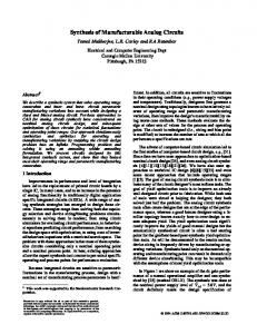
originate from the top one or two atomic layers of a surface; hence, SIMS is a surfacespecific technique. The secondary ions are extracted into a mass spectrometer, which uses electrostatic and magnetic fields to separate the ions according to their mass-to-charge ratio. The ‘dynamic SIMS’ technique, used in this thesis for depth profiling of elements in Si, makes use of a high incidence flux for bulk analysis involving high rates of material removal while providing extreme compositional sensitivity as well. The most obvious advantage of SIMS is the low detection limit. The CAMECA IMS-5f dynamic SIMS is used in this research for surface analysis has a detection limit of ~1013 atoms/cm3. An outstanding feature of SIMS is its ability to constantly monitor and obtain a depth profile of the surface composition with a resolution 450° C. The glass frit wets the surface and then starts to etch or react with the SiNx layer underneath (Fig. 3.14(c)). In addition, the Ag particles begin to sinter and dissolve in the glass frit. Once the glass frit etches through the SiNx film, it starts to etch or dissolve the Si surface underneath the SiNx at temperatures ~670700° C. (Fig. 3.14(d)).
Upon cooling, the excess Si in the glass frit crystallizes
epitaxially, and some of the dissolved Ag in the frit precipitates as Ag crystallites, which get embedded into the Si surface at the Ag-Si interface, forming a direct contact with the Si emitter to provide a path or interconnection for current transport [78] (Fig. 3.14(e)). Finally, lead and possibly other metals also precipitate in the glass layer.
Glass frit
Ag particles forming the bulk of the gridline
Gridline SiNx ARC Emitter n+
Base p
Aluminum
(a) Screen-printed Ag gridline.
77
Glass Glassfrit fritstarts startsmelting to become fluid SiNx ARC n+ emitter
Base p Aluminum
(b) Glass frit starts to become fluid upon heating during the Figure 7(b). Glass frit starts melting upon heating during the contact firing process. fi i
Glass etching through SiNx layer
Sintering and dissolution of Ag in the fluidized glass frit SiNx ARC n+ emitter
Aluminum
Base pp Base
(c) Etching of SiNx layer by the glass frit and sintering of Ag.
78
SiNx ARC n+ emitter
Glass frit etches Si emitter
Base pp Base
Aluminum
(d) Etching of the Si emitter by the glass frit.
Ag gridline
Modified glass after firing SiNx ARC n+ emitter
Re-grown Ag crystallites
Base pp Base
Aluminum
(e) Re-growth of Ag crystallites through the glass layer. Figure 3.14. Screen-printed contact formation.
79
High series resistance is often a problem with screen-printed contacts on solar cells. This is because glass within the Ag paste flows preferentially toward the Ag-Si interface during firing. This creates a glass barrier between the Ag contact and the Si, causing it to be a region of high series resistance in the solar cell [82]. The glassy layer is very continuous and hence the area fraction where Ag grid directly contacts Si is a very small compared to the full area of grid metallization. Low-resistivity contacts can be obtained when the glass does not have sufficient time to flow and collect at the interface during a very short infrared (IR) firing cycle. This would leave a greater number of silver particles at the silicon surface across the entire contact. However, the smaller amount of glass at the interface can cause the IR-fired contacts to have adhesion problems. Even though these ideas are known, no systematic study has been conducted in the literature about controlling or improving the contact interface by tailoring the paste constituents and firing cycle. This provided the motivation in this research to study the role of particle size and glass transition temperatures in tailoring the thickness of the glass layer and size and distribution of Ag crystallites. In addition, special emphasis is placed on rapid thermal firing to constrain the flow of the glass layer to obtain thin regions of glass layers in between Ag crysallites and the Ag grid to promote tunneling. 3.2.2.2 Current Transport Mechanisms Current transport through the SP contacts is very complex and poorly understood at this time.
Several models have been proposed regarding the current transport
mechanism for screen-printed contacts to the Si emitter. Higher series resistance is generally observed for screen-printed contacts compared to evaporated or plated contacts for solar cells because glass acts as a resistive barrier between the Ag grid and the Si.
80
Firor et al. in 1982 first proposed that the current transport occurs via direct Ag-Si interconnections (Fig. 3.15(a)) [82]. However, in 1983 Nakajima et al. observed that annealing of the fired screen-printed contacts in hydrogen reduced the contact resistance of the solar cell [83]. He therefore proposed that the current transport occurs not by direct connection but via tunneling through the fired glass layer between the Ag bulk (grid) and the underlying Si emitter (Fig. 3.15(b)).
Fired Ag gridline
Ag grains
Glass layer
ARC
n+ emitter
Current
p-base (a) Current transports via direct connection to the bulk of the gridline.
81
ARC C u rren t
C u rren t
n+ emitter p-base
(b) Current transport via tunneling through the glassy layer. Figure 3.15. Current transport mechanism in screen-printed contacts. It has been recently shown by transmission electron microscopy that the Si-Ag interface of a fired commercial Ag paste is composed of 200-500 nm-diameter Ag crystallites penetrating the Si by up to 130 nm [80]. These crystallites are surrounded by a quasi-continuous layer of modified glass. A transfer of Ag through a glassy interface has been reported by Schubert et al. [79]. Using conductive cross-sectional atomic-force microscopy (AFM), the contact resistivity between the Ag crystallites and the Si emitter was measured to be ~2×10⁻⁷ Ω-cm2 on average, which is low compared to the typical macroscopic value of contact resistance of 10-3 Ω-cm2 for the whole contact [78]. The interface crystallites are covered by several tens of nanometers of glass frit. This glass frit layer (lead borosilicate glass) has resistivities higher than 109 Ω-cm, which is too high for any conduction through the glass to take place. Thus, he proposed that only a limited fraction of the interface crystallites contributes to the current flow out of the emitter. The conduction thus takes place at isolated spots by two possible mechanisms: (1) by direct
82
metal silicon contact or (2) through ultra-thin regions of a glassy layer via tunneling, with the latter being the more likely situation. Figure 3.16 shows an SEM image of an actual screen-printed and fired Ag contact with glass frit. The glass frit covers a large area at the Ag-Si interface and around the Ag crystallites. Figure 3.17 shows a TEM image of actual screen-printed and fired Ag contact with glass frit. The glass frit covers a large area at the Ag-Si interface, and around the Ag grains and metal precipitates are observed in the glass. A schematic of the cross-section of the fired screen-printed contact is shown in Figure 3.18 along with the possible current transport mechanisms. There is still a considerable lack of understanding of the contact mechanism and current flow in the screen-printed contacts. This provided the motivation to study and correlate the contact interface structure to contact resistance and electrical properties of the contact. In this thesis, the contact interface was varied by altering the paste chemistry and firing conditions, and physical and electrical properties were correlated by a combination of structural and electrical measurements.
Figure 3.16. Ag crystallites re-grown at the interface [17].
83
Ag gridline bulk
Glass frit
Figure 3.17. TEM cross-section image of the screen-printed contact interface: A, B, and C are regions of re-grown Ag crystallites [80]. Tunneling via hopping via metal granules precipitated in the glass
Metal and Si precipitates Glass layer
Direct connection Tunneling through ultrathin glass region
SiNx ARC n+ emitter Ag crystallites
Si
Figure 3.18. Fired screen-printed contact cross-section interface structure showing the possible current transport mechanisms.
3.2.3 Rapid Thermal Processing of Screen-Printed Si Solar Cells Rapid thermal processing (RTP) is used extensively in the microelectronics industry to minimize the thermal budget that a wafer experiences during processing. RTP is also used in this research in conjunction with screen-printed contacts.
In RTP,
processing times are kept very short, and extremely steep temperature ramps are used to avoid unwanted diffusion or oxidation. RTP processing has been investigated in the past few years for Si solar cells. RTP has been successfully demonstrated for industrial-sized
84
Si solar cells along with screen-printed metallization. A simple process involving rapidthermal diffusion and oxidation (each 0.3 µm) than laboratory RTP solar cells to prevent shunting and a high surface concentration of P (>1020 cm-3) to achieve low contact resistance. A throughput of >1,200 wafers/hr is required for all processing steps to meet production line requirements, and hence conventional RTP systems that are designed for single-wafer processing will not meet these requirements. Therefore, continuous RTP systems or belt furnaces have to be designed for the industrial production of Si solar cells. Some manufacturers are currently attempting that [86]. Figure 3.19 illustrates a conventional belt-line furnace. A novel open quartz diffusion system, which combines the advantages of continuous processing of a belt furnace and the cleanliness of closed quartz tube furnaces, is being commercialized [87].
Z1
Z2
Z3
Near IR Heating Lamps Figure 3.19. Belt-furnace processing.
It has been shown that fast ramp-up rates (≥50 °C/s) in RTP produce a good quality, uniform screen-printed Al back-surface field (BSF) [88, 89]. Rapid thermal
85
processing has also been shown to be effective in lifetime and cell efficiency enhancement in low-cost materials because the rapid firing and fast cooling rates enhance the SiNx induced hydrogen passivation of defects [90]. This provided the motivation to explore screen-printed contacts formed by rapid belt speeds in conventional belt furnaces. A systematic study is conducted to see how the belt speed influences not only the contact quality, but also the contact interface structure, including the glass layer thickness, Ag crystallite size and shape, etc.
3.2.4 Screen-Printed Selective-Emitter Cells and Technologies Figure 1.5 in Chapter 1 showed that a 0.7% loss in absolute efficiency can be eliminated by using high sheet-resistance emitters (100 Ω/sq instead of 45 Ω/sq) because of the removal of heavy doping effects in the emitter and improved front-surface recombination technology. This can be done either by making selective emitters or by forming direct screen-printed contacts to the high sheet-resistance emitter.
3.2.4.1 Selective-Emitter Cells Fabricated by Masking and Etching A selective emitter involves two different doping levels, with higher doping (≤40 Ω/sq) underneath the grid to achieve good ohmic contact and low doping between the grid to minimize the heavy doping effect in the emitter. Many different attempts have been made to fabricate selective-emitter solar cells using industrial processes and materials. One technique involves the fabrication of a selective emitter on low-cost polycrystalline silicon by applying a wet etch-back of a heavily doped emitter in the cell area between the gridline fingers. A screen-printed polymeric paste protects the metal fingers during etch-back. The advantages of this process include the use of a full screen-
86
printing technology, phosphorus gettering, and self-alignment. It has been shown that this process can provide improvements of 17 mV in Voc, 1.5 mA/cm2 in Jsc and 1% absolute in efficiency [91]. Another selective-emitter process involves a screen-printed mask after a deep diffusion step (16 Ω/sq), followed by surface texturing combined with etch-back of the emitter [92]. The mask is then removed and a second shallow diffusion is formed (80 Ω/sq) by screen-printing phosphorus paste. This is followed by surface oxidation for passivation purposes, ARC deposition, and metal gridline printing and firing. It is crucial to align the front gridline pattern to the area with the deep emitter without surface texturing. This is achieved with a screen printer with optical alignment. Using a similar principle, another selective-emitter process with a plasma-etch-back technique was developed. In this case, standard commercial screen-printed gridlines are used as a mask for the plasma etch-back of the emitter [93]. A PECVD Si3N4 layer is subsequently deposited for AR coating and good surface and bulk passivation. This process was applied on mc-Si material and a 5% absolute increase in cell efficiency was reported. Similarly, selective-emitter cells have been fabricated on multicrystalline Si using the front metal contacts themselves as masks during hydrogen plasma etches [94]. The plasma also provides diffusion of hydrogen (hydrogenation) while etching, which increases bulk lifetime.
3.2.4.2 Selective-Emitter Cells Fabricated using Self Alignment without Masking and Etching In 1997, for the first time, a process was introduced that could form the selective emitter with only one diffusion step and without additional etching or masking steps [95]. This process involves the selective printing of a phosphorus paste as the front gridline
87
pattern followed by the diffusion process. During the diffusion the P heavily dopes the printed regions, while a shallow high sheet-resistance emitter is formed between the gridlines via auto-doping of the P atoms that are present in the surrounding gas atmosphere as a result of the printed P grid (Fig. 3.20). An ARC layer is deposited (Si3N4 or TiO2) next. Finally, the front-contact metallization is aligned to the P printed pattern and the front and back contacts are co-fired through the dielectric layer. A similar process has been used to realize selective-emitter structures by selective diffusion from a SP P-dopant paste fired in an RTP system [96]. The above processes are time consuming and require several steps or the use of alignment to form the selective emitter. This emphasizes the need to investigate novel techniques for fabricating selective emitter structures or to find ways to make good ohmic contacts to high sheet-resistance emitters.
Out-diffusion of P atoms into the gas phase
P doping paste
Heavy diffusion from the dopant paste
Weak indirect diffusion via the gas phase
Figure 3.20. Screen-printed selective-emitter cells using alignment.
88
3.2.4.3 Selective-Emitter Cells Fabricated using Self-Aligned SelfDoping Ag Paste This technique involves silver that is coated with a layer of dopant and alloyed with silicon. Hence, using this technique, the underlying Si is doped and a low-resistance ohmic contact is formed simultaneously [97]. This concept has been verified by using evaporated Ag with commercially available phosphorus and boron liquid dopants. It was found that the processing temperature should exceed the Ag-Si eutectic temperature of 835° C. This contact system was also implemented using fritless screen-printing Ag paste with self-doping P. It is also possible using a Ag paste with integral P and with a frit to punch through the SiN ARC in a belt furnace to contact n+ layers of up to 100 Ω/sq. Such a contact system is applicable to conventional cell structures like selective emitters and to more complex structures such as interdigitated-back-contact solar cells [98]. As reported in [17] there are two possible routes to achieve good-quality ohmic contacts on lightly doped emitters. First is through self-doping techniques [99] and the second is via optimization of the Ag paste and firing to achieve good ohmic contact directly to a 100 Ω/sq emitter. Since the diffusivity of Ag [100] is greater than that of P [101], the self-doping technique like the one discussed in this subsection involves the risk of junction shunting or introducing an excessive amount of Ag into the emitter region for a longer firing time, which could degrade the open-circuit voltage. Initially the path taken for this thesis research was to employ self-doping pastes; however, it was found that the performance of the p-type FZ cells was limited to 75-80 Ω/sq emitters with low fill factors of ≤0.765. This motivated the research task in this thesis involving the
89
optimization of firing as well as Ag paste inorganic constituents to achieve good screenprinted ohmic contacts directly to high sheet-resistance (100 Ω/sq) emitters.
90
CHAPTER 4 MODELING THE INFLUENCE OF SOLAR CELL PARAMETERS ON PERFORMANCE ENHANCEMENT FROM THE HIGH SHEETRESISTANCE EMITTER 4.1 Introduction This section involves computer modeling and quantitative investigation of the criteria for cell design to maximize the effectiveness of the high sheet-resistance emitter in improving cell performance. This is because bulk lifetime, base resistivity, and front and back-surface recombination velocities can influence the relative improvement from incorporating the high sheet-resistance emitter. If the cell design is not appropriate, the high sheet-resistance emitter can actually degrade cell efficiency. Therefore, it is important to know the cell design criteria before implementing the high sheet-resistance emitter for performance enhancement. The PC1D device-modeling program [102] is used to calculate the performance enhancement from the high sheet-resistance emitter for various cell designs. Table 4.1 shows the key material and device inputs used in the PC1D for these calculations. It is important to note that PC1D is a one-dimensional model; therefore, it can only be used to model the emitter with homogeneous sheetresistance with a constant FSRV. A low minority-carrier lifetime of 30 µs, as opposed to >100 µs, was intentionally used in these initial calculations to assess the potential for efficiency improvement for widely used low-cost low-lifetime silicon substrates.
91
Modeled efficiencies are therefore lower than what they would be for a high-quality single-crystal FZ Si cell where minority-carrier bulk lifetime is generally in excess of 200 µs. In the simulations, the contact quality is assumed to be the same for both high (~100 Ω/sq) and low (40-45 Ω/sq) sheet-resistance emitters, i.e., the series resistance (Rs), shunt resistance (Rsh), and junction leakage current (Jo2) are assumed to be the same for both emitters, which will be shown to be nearly true experimentally in later chapters. Table 4.1: Modeling parameters for the n+-p-p+ solar cells. Device Parameter
PC1D Input 300 µm 1.3 Ω-cm 1000 cm/s
Thickness Resistivity BSRV 40 Ω/sq.conventional cell FSRV 110 Ω/sq.-selective emitter Series Resistance Shunt Resistance J02 n2 Front Surface Reflectance
200 000 cm/s 7000 cm/s 0.6 Ω-cm2 3333 Ω-cm2 5 nA/cm2 2.1 Single Layer ARC: t = 790 Å, n = 2.0 5% None 45 % Diffuse 30 µs
Grid Shadowing Texturing Rear Internal Reflectance Lifetime (τ)
4.2 Device Modeling Results 4.2.1 Effect of Base Resistivity on Performance Enhancement Resulting from the High Sheet-Resistance Emitter The model calculations in Figure 4.1 show the improvements in Voc and in the short-circuit current (Jsc) from the lightly doped emitter, relative to a conventional 40 Ω/sq emitter cell, as a function of base resistivity. Absolute efficiency for the 110 Ω/sq
92
emitter cell as a function of base resistivity is also shown. Lifetime is assumed to be independent of resistivity in these calculations. It is important to note that in these calculations, the back-surface recombination velocity (BSRV) was reduced appropriately for the higher resistivity Si because of the increase in the doping step height (NA+/NA) of the high-low junction. Figure 4.2 shows that for a 30 µs lifetime and 1.3 Ω-cm resistivity material, used in most current industrial cells, a high sheet-resistance emitter of 110 Ω/sq can produce ~0.7% increase in absolute efficiency. A high sheet-resistance emitter (110 Ω/sq instead of 40 Ω/sq) increases the cell efficiency from 15.8% to 16.5% for cell design inputs shown in Table 4.1. Figure 4.3 indicates that the modeled internal quantumefficiency (IQE) shows an appreciable enhancement in the short-wavelength response, which also supports the expected increase in the short-circuit current (∆Jsc) from the high sheet-resistance emitter. 30
17.5
∆ Voc (mV), ∆ Jsc (mA)
A bs olute ef f ic ienc y of a 110 Ω /s q-emitter c ell
20
16.5 16
15 15.5 10
15
∆ V oc 5
110 Ω /sq Cell Efficiency (%)
17
25
14.5 ∆ Js c
0
14 0
5
10 15 Re s is tivity ( Ω -cm )
20
Figure 4.1. The absolute efficiency of a high sheet-resistance emitter solar cell and the change in open-circuit voltage and short-circuit current (relative to a 40 Ω/sq emitter cell) as a function of base resistivity. 93
Figure 4.2 shows that for base resistivities of less than 1 Ω-cm, the improvement in efficiency (∆η) resulting from the high sheet-resistance emitter is very rapid. For resistivities between 1 Ω-cm and 10 Ω-cm, there is almost a linear improvement in efficiency with the decrease in resistivity. However, for resistivities greater than 10 Ωcm, the efficiency improvement saturates at 0.4% absolute (for the 30 µs bulk lifetime case).
∆η (%)
1.6 1.4
bulk lifetime = 200 us
1.2
bulk lifetime = 30 us
1 0.8 0.6 0.4 0.2 0 0
5
10
Base Resistivity (Ω -cm)
15
20
Figure 4.2. Improvement in cell efficiency resulting from the high sheet-resistance emitter relative to the conventional 40 Ω/sq emitter. 100 90 80 70
IQE (%)
60 50 40
improvement in Jsc due to the improved blue response
30
110 ohm/sq emitter
20
40 ohm/sq emitter
10 0 300
500
700
900
1100
wavelength (nm)
Figure 4.3. PC1D-modeled IQE plots for high- and low-sheetresistance emitters. 94
The efficiency enhancement starts to saturate starting at lower base resistivities (6 Ω-cm) for the higher bulk lifetime case. This is because the effect of the base recombination starts to become more dominant for higher minority-carrier diffusion lengths, where minority carriers become more sensitive to the recombination in the base. The emitter and base saturation current densities (Joe and Job, respectively) in Figure 4.4 reveal that above 10 Ω-cm resistivity, Jo (=Joe+Job) is dominated by Job, which is the same for both high and low sheet-resistance emitters cells. Therefore, Jo, Voc, and efficiency do not change with base resistivity, and the efficiency enhancement becomes saturated and limited only by the increase in short-circuit current (Jsc) due to the reduced Auger recombination in the emitter. Model calculations were extended further to extract the emitter and base component of the saturation current density, i.e., Joe and Job. Figure 4.4 shows that above 10 Ω-cm resistivity, Job is much greater than the Joe of the high and low sheet-resistance emitter. Therefore, the open-circuit voltages of both cells are virtually identical. As we lower the base resistivity below 10 Ω-cm, Job decreases. Since the Joe of the 40 Ω/sq emitter cell is higher than that of the 110 Ω/sq emitter cell and is not negligible relative to the Job, Jo = Joe + Job of the conventional cells becomes higher, while the Jo of the high sheet-resistance-emitter cell remains ≈Job. As a result, the efficiency enhancement resulting from the high sheet-resistance emitter rises as we decrease the resistivity below 10 Ωcm (Fig. 4.2). It should be noted that the bulk lifetime was maintained at 30 µs for all resistivities in these calculations.
95
680
Joe for a 110 ohm/sq emitter Joe for a conventional 40 ohm/sq. emitter Job Voc for a 110 ohm/sq emitter Voc for a conventional emitter 40 ohm/sq.
660
1E-11
640 620
1E-12 600 580
1E-13
Open-circuit voltage Voc (mV)
Saturation Current (A)
1E-10
560 1E-14
540 0
5
10
Resistivity (Ω -cm)
15
20
Figure 4.4. Plots of the leakage currents (Joe and Job) and open-circuit voltage (Voc) for the high and low sheet-resistance emitters.
4.2.2 Effect of Front-Surface Passivation on Performance Enhancement Resulting from the High Sheet-Resistance Emitter The model calculations in Figure 4.5 show that the front-surface recombination velocity (FSRV) is also very critical in realizing the full benefit of the high sheetresistance emitter. In these calculations, bulk lifetime, BSRV, and base resistivity were fixed at 30 µs, 1,000 cm/s, and 1.3 Ω-cm, respectively. The FSRV of the conventional cell was fixed at 200,000 cm/s, while the FSRV for the 110 Ω/sq emitter cell was varied from 103-106 cm/s.
The calculations indicate that for an FSRV greater than
120,000 cm/s, the high sheet-resistance emitter actually under performs the conventional cell because a transparent emitter (emitter thickness < 3 × diffusion length) with high
96
FSRV lowers the Voc and Jsc. However, if the FSRV of the 110 Ω/sq emitter can be lowered to 10,000 cm/s, the role reverses and the 110 Ω/sq emitter increases the performance by 0.60% absolute. The crossover point is a function of the FSRV selected for the conventional 40 Ω/sq emitter (2×105 cm/s used in these calculations). If the FSRV value for 40 Ω/sq emitter is increased from 200,000 cm/s to 500,000 cm/s, the curve becomes almost asymptotic with the FSRV axis, with the crossover point approaching 106 cm/s. The FSRV value for the 40 Ω/sq emitter was fixed at 200,000 cm/s in these calculations, while the FSRV for the 110 Ω/sq emitter was varied because heavily doped emitters are less sensitive to the front-surface passivation [103]. The FSRV of 200,000 cm/s also represents typical passivation for conventional screen-printed SiNx-coated 40 Ω/sq emitter cells. Model calculations also showed that the improvement in efficiency from the high sheet-resistance emitter for a FSRV0.78. The series resistance of a screen-printed Si solar cell is often dictated by the front-contact resistance [82] for screen-printed cells. Thus, the effect of the specific contact resistance on the loss in FF was also calculated using the grid model in [104] for comb-like front Ag grid design on a 2×2 cm2 solar cell. 100
The derivation and calculation for the specific contact resistance induced loss in FF is given in Appendix C.1. Calculations in Figure 4.10, reveal that the specific contact resistance needs to be below 3 mΩ-cm2 to avoid any appreciable loss in FF. A specific contact resistance greater than 10 mΩ-cm2 significantly increases the loss in FF.
0.84
Jo2=1e-7, (n2=2),Rsh=3.33e4 Jo2=4e-8 (n2=2), Rsh=3.33e4 Jo2=1e-8 (n2=2). Rsh=3.33e4 Jo2=1e-9 (n2=2), Rsh=3.33e4
0.82
FF
0.8 0.78 0.76 0.74 0.72 0
0.1
0.2
0.3
0.4
0.5
0.6
Rs (Ω -cm 2)
0.7
0.8
0.9
1
Figure 4.8. The effect of Rs and Jo2 on FF. 0.83 0.81
Jo2=1e-9 Jo2=3.00E-08 Jo2=1.00E-07
Jo2=1e-8 Jo2=5.00E-08 Jo2=2.00E-07
0.79 0.77
FF
0.75 0.73 0.71 0.69 0.67 0.65 100
1000
10000
Rsh (Ω -cm 2)
100000
1000000
Figure 4.9. The effect of Rsh and Jo2 on FF. Rs is set to 0.6 Ω-cm2. 101
0.08 0.07 0.06 ∆ FF
0.05 0.04 0.03 0.02 0.01 0 0.01
0.1 1 10 100 Specific contact-resistance (m Ω -cm 2)
Figure 4.10. The effect of specific contact resistance on the loss in FF.
4.3 Conclusions Model calculations were performed in this chapter to provide guidelines for achieving maximum benefit from the high sheet-resistance emitter. In addition, requirements for contact parameters were established for achieving FFs in excess of 0.78. These calculations and guidelines are used to design the experiments in the following chapters. Model calculations revealed that the front-surface recombination velocity should be 200 µs are used for all the experiments in this chapter to maximize the enhancement in absolute cell efficiency using a high sheet-resistance emitter. Silicon wafers were first chemically cleaned, followed by POCl3 diffusion to form the n+-emitter. The diffusion temperature used for the 45 Ω/sq emitter was 889° C, while that for the 100 Ω/sq emitter was 857° C. All other parameters were kept the same for both diffusions. After the phosphorus-glass removal and another clean, a PECVD SiNx AR coating was deposited on the emitter. The optimization study was done for the 100 Ω/sq emitter using a high-frequency (13.56 MHz) direct PECVD SiNx passivation layer deposited at 300° C. A low-frequency (50 KHz) direct PECVD SiNx film deposited at 430° C, which gives superior surface passivation, was also used for comparison. Next, an Al paste was screen printed on the back side and dried at 200° C. The Ag grid was then screen printed on top of the SiNx film and Ag and Al contacts were co-fired (single firing step) in a lamp-heated belt furnace. The Radiant Technology Corp. model LA-310 belt furnace used in this study has three heating zones, with lengths of 7.5, 15, and 7.5 inches, respectively, totaling 30 inches for all three hot zones. The cells were then isolated using a dicing saw and annealed in forming gas at 400° C for ~15 min. No surface texturing was used for these cells. In addition to the PV168 Ag paste from Dupont, two additional commercial Ag 106
pastes (A and B) were also investigated, which are widely used in production for low sheet-resistance emitter cells. All three pastes contain phosphorus dopant. In addition to the 100 Ω/sq emitter cells, conventional cells with a 45 Ω/sq emitter were also fabricated using an optimized co-firing scheme for each paste. To understand and compare the quality of contacts for the three different pastes (A, B, and PV168) on the low and high sheet-resistance emitters, current voltage (I-V) and internal quantum efficiency (IQE) measurements were taken to extract cell parameters and the short- and long-wavelength response.
Suns-Voc measurements [29] were used to evaluate the junction leakage
current (Jo2), which is generally attributed to the recombination centers in the depletion region [107]. Jo2 was determined by fixing the second-diode ideality factor (n2) to two. Since high-quality monocrystalline FZ Si, which has very few dislocations and impurities, was used in this study, the degradation in Jo2 primarily attributed to the recombination centers created in the depletion region by the paste and firing conditions. SIMS measurements were performed on selected samples to determine the Ag and P concentration profiles in the silicon directly underneath the Ag grid using a CAMECA IMS-5F ion microscope. The Ag grid was etched in HCl prior to the SIMS measurements to prevent any Si etching. The samples were bombarded with 5.5 KeV O2+ primary ions for analysis of Ag, while 14.5 KeV Cs+ primary ions were used for P. The primary ion beam was rastered over an area of 150 µm × 150 µm. Positive or negative secondary ions were collected from a ~20 µm diameter area in the center of the rastered crater for Ag and P, respectively. Spreading resistance measurements were made to determine the electrically active P concentration profile in the emitter. Finally, the contact resistance measurements were made using transfer-length method (TLM) patterns
107
[33], which were printed during cell fabrication. Since screen-printed (SP) contacts are not full area metal-Si contacts, the TLM of measurement gives a macroscopic specific contact resistance (ρcm) for SP contacts. The actual temperature of the wafer was measured as it was fired through the belt by attaching a fast-response K-type thermocouple with a closed-end tip loosely touching the surface of the wafer. This is because set temperature and sample temperature are quite different in a belt furnace. Table 5.1 shows the approximate peak firing temperatures for the corresponding set temperature and belt speed for the different firing cycles used in this study. Table 5.1: Set temperature, belt speed and the approximate peak temperature experienced by the cell. Set temperature (°C) 435/585/750°C 825/825/825°C 850/850/850°C 900/900/900°C 900/900/900°C 900/900/900°C
Belt speed (ipm) 15 80 80 80 60 15
Approximate peak temperature (°C) 720 750 780 835 850 895
5.3 Results and Discussion 5.3.1 Determination of the 45 and 100 Ω/sq Emitter Doping Profiles The emitter profile can greatly influence solar cell characteristics such as junction shunting, grid contact resistance, and short-wavelength IQE response [104].
For
example, the specific contact resistance (ρc) and emitter sheet resistance (ρs) are inversely proportional to the surface dopant concentration (ND), while for a well-passivated surface, Joe and the photo-current loss are directly proportional to ND and the doping profile. The junction depth also influences the junction shunting (Rsh) for screen-printed contacts, with a shallow junction being more vulnerable to contact firing-induced
108
degradation. Thus, there are competing factors in designing the emitter region for highefficiency cells. Therefore, to gain a better understanding of the cell performance results, emitter-doping profiles were first determined by spreading resistance measurements. Figure 24 shows the phosphorus doping profiles for the 100 and 45 Ω/sq emitters formed in this study. The 100 Ω/sq emitter had a surface concentration of ~1.5×1020 cm-3 with a junction depth of 0.277 µm, while the 45 Ω/sq emitter had a surface concentration of ~2.3×1020 cm-3 with a junction depth of 0.495 µm. With a good surface passivation, the 100 Ω/sq emitter should lead to higher current because of the thinner heavily doped dead layer compared to the 45 Ω/sq emitter (Figure 4.5). On the other hand, shallow emitters are more prone to junction shunting or leakage because of the incorporation of impurities from the paste into the junction, especially if the frit in the paste strongly etches the Si surface to allow the Ag metal to reach the junction. Junction shunting lowers the opencircuit voltage (Voc) and the FF of the cell, as shown by the model calculations in the previous chapter. According to the literature [108, 109], a surface dopant concentration of >1019 cm-3 is required for an evaporated and full-area ohmic contact to an n-type Si region. However, it has been shown by SEM and TEM studies that full-area metal-Si contact is not achieved for the screen-printed grid because of the presence of a quasi-continuous glass frit layer (Figs 3.16 and 3.17 in Chapter 3). It is conjectured that carriers have to tunnel through the glass layer [17, 78, 80]. That is why it is difficult to achieve excellent ohmic contacts using screen-printing technology. Figure 5.1 shows that both the 45 Ω/sq and 100 Ω/sq emitters used in this study have high surface concentrations greater than 1×1020 cm-3. However, the challenge is to develop an appropriate firing condition that
109
will provide adequate area coverage for the contact points (Ag crystallites) to the 100 Ω/sq emitter without shunting or degrading the junction.
Therefore, a study was
conducted to optimize contact firing conditions that can yield good contact quality for both 45 and 100 Ω/sq emitters using three different commercial pastes A, B, and PV168. These three pastes have been evaluated with the goal of achieving a performance enhancement from the 100 Ω/sq emitter over the 45 Ω/sq emitter, in addition to establishing the requirements for paste composition for achieving good contacts to high sheet-resistance emitters. 1.E+21
P Concentration (cm -3)
100 Ohm/sq. emitter 45 Ohm/sq. emitter
1.E+20
1.E+19
1.E+18
1.E+17
1.E+16 0
0.1
0.2
0.3
0.4
0.5
Depth (µ m)
Figure 5.1 Spreading resistance profiles of POCl3 diffused 100 Ω/sq and 45 Ω/sq emitters. Achieving a good ohmic contact between the Ag and the high sheet-resistance Si emitter is a challenge because it has a lower P doping (Fig 5.1), resulting in higher specific-contact resistance for a tunneling-based carrier transport process described by the following equation [110]:
110
2 ε m* s h
ρ c ∝ exp
φ Bn N D
(5.1)
where ND is the doping concentration (≥1019 cm-3), m* is the effective mass of the charge carriers, εs is the semiconductor permittivity, ħ is the reduced Planck constant, and φB is the Schottky barrier height. The surface doping for both the 45 and 100 Ω/sq emitters used in our cell process is greater than 1019 cm-3. However, the high sheet-resistance emitter is shallower (0.277 µm) than the low sheet-resistance emitter (0.495 µm). Hence, the challenge is to achieve good ohmic contacts without degrading or shunting the p-n junction. This requires the technology development and optimization of the glass frit, Ag powder in the paste, and contact firing, which are described in the following sections.
5.3.2 Optimization of Ag Paste Firing to Achieve Good Contacts on a 100 Ω/sq Emitter 5.3.2.1 Effect of Conventional Firing of Commercial Pastes A and B on the Performance of 45 Ω/sq and 100 Ω/sq Emitter Cells Before investigating the PV168 paste from Dupont, we studied the two widely used commercial Ag pastes, A and B. Both pastes are expected to give good-quality contacts to 45 Ω/sq emitters. Complete cells were fabricated and characterized. Light and dark I-V and Suns-Voc data is summarized in Table 5.2, which confirms that conventional co-firing of pastes A and B at 700-750° C peak temperature gives excellent FFs, exceeding 0.785 for the 45 Ω/sq emitter cells, with efficiencies approaching 16%.
111
Table 5.2: I-V data for cells fabricated with commercial pastes A and B using co-firing processes on a low sheet-resistance (45 Ω/sq) emitter. Paste
Co-firing Process
Voc (mV)
Jsc (mA/ cm²)
FF
Eff (%)
n factor
Rs (Ωcm²)
Rsh (Ωcm²)
ρcm (mΩcm²)
Jo2 (nA/ cm2)
A
435/585/750°C 15 ipm
623
31.80
0.792
15.7
1.04
0.61
22,541
0.12
13
627
32.6
0.785
16.0
1.09
0.64
188,04 0
0.38
29
B
850/850/850°C 80 ipm
Currently, no cell manufacturer uses high sheet-resistance emitters (≥ 60 Ω/sq) because it is difficult to achieve good screen-printed ohmic contact using conventional Ag pastes. Thus, different firing conditions were used to investigate the performance of pastes A and B on the 100 Ω/sq emitter. To understand the significant difference in efficiency and FFs for the two sheet resistances, specific-contact resistance (ρc) measurements were taken by the TLM method. It is important to recall that the model calculations in Chapter 4 revealed that the specific-contact resistance should be below 3 mΩ-cm2 to achieve good FFs. In addition, Jo2 and series resistance (Rs) should be below 50 nA/cm2 and 1 Ω-cm2, respectively, to achieve FFs≥0.77. It was found that both commercial pastes worked well for the 45 Ω/sq emitter, but failed on the 100 Ω/sq emitter for various firing schemes (Table 5.3). This was the result of very high contact resistance at lower firing temperatures and high junction-leakage current and lower Voc at higher firing temperatures (Table 5.3). This indicates that the composition of pastes A and B is not adequate to make good ohmic contacts to the high sheet-resistance emitter, regardless of the firing scheme. Therefore, as explained in the next section, we acquired a less aggressive special paste (PV168) from DuPont that allowed us to go to higher firing temperatures without causing junction shunting.
112
Table 5.3: I-V data for cells fabricated with commercial pastes A and B using co-firing process on a high sheet-resistance (100 Ω/sq ) emitter for different firing temperatures. Paste Firing Temperature (°C)
Voc (mV)
Jsc (mA/cm²)
FF
Eff (%)
n factor
Rs (Ωcm²)
Rsh (Ωcm²)
ρcm (mΩcm²)
Jo2 (nA/ cm2)
Paste A 435/585/750° C15 ipm
612
32.1
0.704
13.9
1.09
2.41
1,707
33.00
10
825°C/80 ipm
633
32.3
0.268
5.5
1.31
13.39
644
12.51
11
850°C/80 ipm
618
33.5
0.740
15.3
1.07
1.78
1,247
7.21
106
900°C/80 ipm Paste B 825°C/80 ipm
620
33.2
0.761
15.6
1.10
1.05
5,092
1.14
29
626
18.7
0.231
2.7
1.42
29.70
6,658
200
15
850°C/80 ipm
291
32.7
0.479
4.6
2.02
1.11
3,071
1.53
120,000
900°C/80 ipm
572
32.9
0.536
10.1
2.62
3.21
15,078
2.30
697
5.3.2.2 Optimization of Firing Conditions for PV168 Ag Paste to Achieve Good Contacts on 100 Ω/sq Emitters The paste composition and firing cycle can significantly influence series resistance, junction leakage, and FF. The previous section showed that the widely used commercial pastes failed on the 100 Ω/sq emitter over a wide range of practical firing conditions. Therefore, PV168 paste was used in which the composition, shape, and size of the frit and Ag particles were tailored to reduce the etching of Si at high temperatures. Exact details about the paste chemistry are proprietary. The following sections describe the understanding and optimization of firing temperature and belt speed that led to the firing conditions, which eventually produced for the first time good contacts directly to the 100 Ω/sq emitter. First, the effect of firing temperature on FF was examined using a high belt speed (≥80 ipm), referred to as spike firing in this thesis. Table 5.4 shows that specific-contact
113
resistance (ρc) decreases with higher firing temperature and reaches ~1 mΩ-cm2 at a set temperature of 900° C, resulting in a high FF of 0.775. Notice that the Voc did not degrade even for such a high set temperature. This is supported by very low junction leakage current (Jo2) of 10 nA/cm2. It is important to realize that the actual sample temperature is generally lower than the set temperature (Table 5.1), especially for high belt speeds.
Temperature profiling showed that the sample experienced a peak
temperature in the range of 830-840° C for a few seconds during the spike firing cycle of 900° C/80 ipm. Table 5.4: I-V data for cells fabricated with PV168 Ag paste using co-firing process (80 ipm belt speed) on a high sheet-resistance (100 Ω/sq ) emitter for different firing temperatures. Set Temperature (°C)
Voc (mV)
Jsc (mA/cm²)
FF
Eff (%)
n factor
Rs (Ω-cm²)
Rsh (Ω-cm²)
ρcm (mΩcm²)
825°C
626
19.8
0.249
3.1
1.46
27.16
2,951
45.00
850°C
572
32.9
0.536
10.1
2.62
3.21
15,078
4.71
900°C
627
33.9
0.775
16.5
1.01
1.00
3,353
1.06
Since the combination of the set temperature and belt speed dictates the thermal budget of the sample, we also examined the role of belt speed on contact formation. Table 5.5 shows that increasing the belt speed from 15 to 80 ipm at a fixed set temperature of 900° C lowered Jo2 by a factor of 100. The reduction of Jo2 agreed well with the improvement in the FF and Voc, also shown in Table 5.5. The optimum firing condition for the PV168 paste was found to be 80 ipm at 900o C, which gave a FF of 0.775 and the best cell performance of 16.5% with a Voc of 627 mV. The firing cycle optimization was done up to a set temperature of 900° C because of the limitations of the
114
Radiant Technology Corp. model LA-310 belt furnace used in this study, which could not maintain set temperatures greater than 900° C for speeds of 80 ipm or higher. Table 5.5: I-V data for cells fabricated with PV168 Ag paste using co-firing process (900°C set temperature) on high sheet-resistance (100 Ω/sq ) emitters for different belt speeds. Belt speed (ipm)
Voc (mV)
Jsc (mA/ cm²)
FF
Eff (%)
n factor
Rs (Ωcm²)
Rsh (Ωcm²)
ρcm (mΩcm²)
Jo2 (nA/cm2)
15
578
32.8
0.564
10.7
3.63
0.65
13,316
2.78
1,070
60
623
33.4
0.759
15.8
1.03
1.27
979,127
4.67
15
80
627
33.9
0.775
16.5
1.01
1.00
3,353
1.06
10
5.3.2.3 SIMS Analysis to Understand and Explain the Success of PV168 Ag Paste in Forming Good Ohmic Contact to 100 Ω/sq Emitter Secondary ion mass spectroscopy (SIMS) was performed to determine the extent of Ag migration into Si by obtaining Ag profiles into the Si emitter. The SIMS data in Figure 5.2 show that Ag indeed penetrates into Si and could be a problem for junction shunting. It was found that slow belt-speed firing (15 ipm) at a set temperature of 900° C resulted in a much higher concentration of Ag in the underlying Si, while fast firing (80 ipm) introduced a much lower amount of Ag at or near the p-n junction. Recall that spreading resistance measurements gave a junction depth of 0.277 µm for the 100 Ω/sq emitter (Fig. 5.1). Ag concentrations at the n+-p junction (0.277 µm) were found to be 6×1018 cm-3, 2×1017 cm-3, and 2×1016 cm-3 for belt speeds of 15, 60, and 80 ipm, respectively. This indicates that faster firing decreases the Ag concentration near the junction edge, which in turn reduces junction leakage current and gives higher Voc. This is consistent with the work of Van Craen et al. [111], who showed that solar cell efficiency decreases with the increase in Ag concentration near the junction.
115
1.E+23 Ag profile for 15 ipm firing
Ag Concentration (cm -3)
1.E+22
Ag profile for 60 ipm firing
1.E+21
Ag profile for 80 ipm firing
1.E+20 1.E+19 1.E+18 1.E+17 1.E+16 1.E+15 0.0
0.1
0.2
Depth (µ m)
0.3
0.4
p-n junction
Figure 5.2. SIMS profile of PV168 Ag paste fired at different belt speeds.
In Section 5.3.2.1 it was shown that pastes A and B did not show a performance enhancement with the 100 Ω/sq emitter for various firing conditions. Instead, cell performance degraded because of either high contact resistance or excessive junction leakage current. On the other hand, in Section 5.3.2.2 it was demonstrated that the PV168 Ag paste is capable of producing high FFs and cell efficiencies on 100 Ω/sq emitters, provided spike firing is performed at a high set temperature, resulting in sample peak temperatures in the range of 830-840° C for a very short time (a few seconds). PV168 is made by DuPont using a proprietary technology involving a somewhat different Ag particle morphology, Ag content, and frit composition. The SIMS analysis is illustrated in this section to complement cell data to understand and explain why, in contrast to PV168 paste, pastes A and B were not able to achieve high FFs on the 100 Ω/sq emitter. To improve the understanding further, more cells were fabricated on the 100 Ω/sq emitter using pastes A, B, and PV168 and the same co-firing condition (900°
116
C/80 ipm).
Table 5.6 shows that the Voc and FF decrease, while Jo2 increases
monotonically for cells made from pastes PV168, A, and B, respectively. The lowest Jo2 value of 10 nA/cm2 for the PV168 paste indicates much less junction shunting compared to the other two pastes.
This was supported by SIMS analysis showing the Ag
concentration at the junction edge (Table 5.6) to be 1.24×1016 cm-3, 2.50×1017 cm-3, and 1.20×1018 cm-3. Thus, the Ag penetration into Si is reduced significantly because of the PV168 paste chemistry, permitting high-temperature firing to reduce contact resistance without increasing the Jo2 value for the shallow 100 Ω/sq emitter. Table 5.6: Correlation of Voc, FF, and Jo2 with Ag concentration at the junction for pastes PV168, A, and B using co-firing process (900° C set temperature and 80 ipm belt speed) on high sheet-resistance (100 Ω/sq ) emitters. Paste
Voc (mV)
FF
Jo2 (nA/cm2)
Ag concentration at the junction (cm-3)
ρcm (mΩ-cm²)
PV168
627
0.775
10
1.24×10¹⁶
1.06
A
619
0.761
29
2.50×10¹⁷
1.14
B
572
0.536
697
1.20×10¹⁸
2.30
To improve the understanding of the series resistance effect of the three pastes, specific-contact resistance measurements were made.
Table 5.6 shows that the
macroscopic specific-contact resistance for all three pastes was less than 3 mΩ-cm2 on the 100 Ω/sq emitter, which is acceptable for screen-printed contacts and should not degrade the FF. For the 100 Ω/sq-emitter cells, PV168 gave the lowest specific-contact resistance (1.06 mΩ-cm2), followed by paste A (1.14 mΩ-cm2) and paste B (2.3 mΩcm2). These results indicate that, contrary to the original concern, the problem with conventional pastes A and B is not the contact resistance to the 100 Ω/sq emitter. Instead,
117
when we go to high temperatures (set temp. ~900° C) to achieve reasonable contact resistance, the Ag penetration into the junction becomes excessive, which increases the Jo2 and lowers the Voc (Table 5.3). On the other hand, if we stay at lower temperatures (set temp.≤ 850° C) to prevent excessive Ag penetration, the contact resistance becomes too high and degrades the FF and cell performance as shown in Table 5.3.
The
composition of PV168 is such that at higher firing temperatures (830-840° C), good ohmic contact is achieved, probably because of the larger number and/or size of Ag crystallites in contact with the emitter surface.
In addition, the frit content and
composition are such that PV168 is able to etch through the SiNx AR coating without excessive etching of the Si emitter underneath the grid. In the case of the PV168 paste, Ag penetration into Si is somewhat arrested because of the right combination of frit content and composition and the Ag particle morphology.
The contact formation
mechanism [64, 76] for widely used commercial pastes generally involves lower temperature firing (700-800° C), heating-induced fluidization of the glass frit, and surface wetting, followed by etching of the AR coating and the Si emitter surface. Higher firing temperature results in deeper etching of Si and higher Ag penetration. It appears that in the case of PV168, the etching of Si by the frit is minimal and the contact formation takes place via a very thin eutectic region or Ag-Si alloy. SIMS measurements were also taken to obtain the phosphorus profiles before and after the grid formation and gain a better understanding of the success of PV168 screenprinted contacts on 100 Ω/sq emitters. Ag metal was etched off prior to the SIMS measurements.
For the optimized firing condition of PV168, SIMS measurements
showed no apparent addition of P from the paste to the original 100 Ω/sq emitter profile
118
(Fig. 5.3), even though the paste contains some source of phosphorus. This indicates that the injection of P from the paste did not play a major role in the ohmic-contact formation to the 100 Ω/sq emitter. However, to establish this with more certainty we did the contact firing on the undiffused wafer; we found that after firing, some additional P does come from the paste, but the profile is very shallow, with a surface concentration of only ~4×1018 cm3, resulting in a sheet resistance of ~5000 Ω/sq. Thus, there is no indication of selective-emitter formation. SIMS measurements of the P profiles were taken underneath the Ag grid and underneath the silicon nitride coating to get an idea of the extent of Si emitter etching during contact formation. The difference between the two profiles shown in Figure 5.3 reveals a penetration depth of ~55 nm for the PV168 Ag paste fired at 900° C/80 ipm, which could also be a measure of the average penetration depth of the Ag crystallites into Si. This is much less than the average penetration depth of 130 nm for the Ag crystallites formed in conventional pastes [78].
-3
P Concentration (cm )
1.00E+21
P emitter profile underneath the SiNx layer only
1.00E+20
P emitter profile underneath the PV168 metal grid
1.00E+19 1.00E+18 1.00E+17 1.00E+16 0.00
0.10
0.20
0.30
0.40
Depth (µm)
Figure 5.3 P emitter 100 Ω/sq profiles underneath the SiNx layer only and underneath the PV168 Ag metal contact grid after contact firing.
119
5.3.3 Quantitative Assessment and Enhancement of Si3N4-induced Front- Surface Passivation on 45 and 100 Ω/sq Emitters 5.3.3.1 Internal Quantum Efficiency (IQE) Analysis to Support Current Enhancement Due to the High Sheet-Resistance Emitter In the previous sections, we successfully demonstrated for the first time that good-quality screen-printed contacts can be directly achieved on a 100 Ω/sq emitter with good ohmic contact, fill factor, and cell efficiency.
Figure 5.4 shows the internal
quantum efficiency (IQE) plots of a conventional 45 Ω/sq cell fabricated using silver paste B (Cell 1), and the 100 Ω/sq emitter cell co-fired using PV168 paste (Cell 2). The short-wavelength response of Cell 2 is superior because the 0.277 µm deep lightly doped emitter reduces the dead layer thickness, Auger recombination, and the heavy doping effects. The extraction of Jsc via photon flux weighted integration of the IQE curve in Figure 5.4 showed that the difference in the short-wavelength response accounts for the great majority of the observed 1.3 mA/cm2 improvement in Jsc for the two cells. There is a slight difference in the long-wavelength response in favor of the 100 Ω/sq emitter cell fired at higher temperature. Since co-firing is normally performed at lower temperatures, around ~750° C, for conventional 45 Ω/sq cells to avoid junction shunting, a slightly lower-quality back-surface field (BSF) may result. This may explain why the longwavelength response for Cell 2 is slightly superior to that of Cell 1. By matching the experimental and calculated long-wavelength IQE, using the PC1D model [102], effective BSRVs were estimated to be 600 cm/s and 900 cm/s for the co-fired 100 Ω/sqand 45 Ω/sq emitter cells, respectively. A similar analysis for the short-wavelength response gave an effective FSRV of 250,000 cm/s and 450,000 cm/s for the 100 and 45 Ω/sq emitters, respectively. Thus, co-firing with PV168 Ag paste on the 100 Ω/sq emitter
120
at a set temperature of 900° C with a high belt speed of 80 ipm accomplishes reduced FSRV, reduced emitter recombination, an effective BSF, and a good ohmic contact to 100 Ω/sq emitters. Model calculations show that a BSRV of 600 cm/s can limit the maximum possible Voc to ~662 mV for a 0.6 Ω-cm material with a bulk lifetime of 250 µs
when
the
effect
of
FSRV
(Voc=(kT/q).ln[(Jsc/(Joe+Job)) +1]).
or
Joe
on
Voc
is
completely
neglected
The cell data in Figure 5.4 also show that the
efficiency difference of ~0.5% between the co-fired 45 Ω/sq cell and the 100 Ω/sq cell is mainly due to higher short-wavelength response or Jsc. 100 90 80
Cell 1: Co-firing process using paste B on 45 Ohm/sq emitter with poor surface passivation
IQE (%)
70 60
Cell 2: Co-firing process using PV168 on 100 Ohm/sq emitter with poor surface passivation
50
Cell 3: Co-firing process using PV168 on 100 Ohm/sq emitter with good surface passivation
40 30 20 10 0 300
Cell ID 1 2 3
Voc (mV) Jsc (mA/cm2) 627 32.6 627 33.9 642 34.6 500
700
FF 0.785 0.775 0.771 900
Wavelength (nm)
Eff (%) 16.0 16.5 17.1 1100
Figure 5.4. IQE plots for co-fired 45 Ω/sq emitter (using paste B) and 100 Ω/sq emitter cells using PV168 paste with good and poor frontsurface passivation.
121
5.3.3.2 Further Enhancement in the Performance of 100 Ω/sq-Emitter Cell with Higher Quality Front-Surface Passivation All the cells reported in the previous sections had a SiNx film deposited in a highfrequency (HF) PECVD reactor, which resulted in an effective FSRV of ~250,000 cm/s on the 100 Ω/sq emitter and ~450,000 cm/s on the 45 Ω/sq emitter. These FSRV values were obtained by matching the measured and PC1D-simulated IQEs in the shortwavelength range (0.3-0.5 µm). The actual emitter doping profile was used with the default bandgap narrowing model of PC1D. According to the model calculations in Chapter 4, these FSRV values are too high to obtain maximum benefit from the high sheet-resistance emitter. To enhance the understanding of this aspect and increase the efficiency gap between the 100 and 45 Ω/sq- emitter cells, we improved the surface passivation by depositing a low-frequency (LF) PECVD SiNx,. The deposition condition (430-435°C) was used to achieve better passivation. The IQE/PC1D analysis showed that the LF SiNx lowered the effective surface recombination velocity of the 100 Ω/sq emitter from ~250,000 cm/s to ~40,000 cm/s. This should lower Joe and give higher Voc [=kT/q⋅ln(Jsc/Jo1 + 1)] because Jo1 = Joe+ Job. Recall that in this study, low-resistivity Si was selected to reduce the base saturation current density (Job), which made Voc more sensitive to Joe. Figure 5.4 shows that indeed the co-fired 100 Ω/sq cell using PV168 Ag paste (Cell 3) with good surface passivation gave ~1% higher cell efficiency with a much higher blue response of 2.0 mA/cm2, higher Jsc, and 15 mV higher Voc compared to the co-fired 45 Ω/sq cell with poor surface passivation. It also gave ~0.6% improvement in absolute efficiency over the poorly passivated 100 Ω/sq cell. The FSRV for the wellpassivated (LF SiNx) cell was comparable to that of Kerr et al., who reported an FSRV of
122
~25,000 cm/s for an emitter with a surface concentration of 1.8x1020 cm-3 [112]. It has been shown in [113] that annealing at 500° C causes Joe to decrease by a factor of two for 100 Ω/sq emitters passivated with LF direct-plasma SiNx film, while the Joe for the HF direct-plasma SiNx film increases during annealing. It is important to note that because of our HF PECVD machine limitations, the HF SiNx deposition conditions were not optimum for a good FSRV. The conditions for better HF SiNx passivation include higher deposition temperature of 400° C (the deposition temperature of our HF PECVD machine is 300°C) and higher gas flows [31]. The beneficial effect of the LF SiNx is especially pronounced after rapid high-temperature firing. This is supported by the measured Joe values, which showed a drop from 580 fA/cm2 to 66 fA/cm2 after firing. This result is close to the Joe values below 60 fA/cm obtained for good surface passivation using optimized remote or HF PECVD SiNx for surface concentrations up to 1020 cm-3 (without annealing) [114]. The short-wavelength response can be further enhanced by using a stack oxide/nitride front-surface passivation since a thermal oxide is known to passivate defects and dangling bonds at the surface. Figure 5.5 shows a higher IQE short-wavelength response for a stack 100 Å rapid thermal oxide (RTO)/LF PECVD SiNx film (see Appendix D for the oxide growth process conditions) compared to a LF SiNx film only. The lowest Joe (54 fA/cm2) was measured for the stack RTO/SiNx front-surface passivation, which supports the higher short-wavelength response.
123
100 95 90
IQE (%)
85 80 75 70 65
Stack RTO/LF SiN passivation
60
LF SiN passivation only
55 50 330
380
430
480
530
580
Wavelength (nm)
Figure 5.5: Short-wavelength IQE response for 100 Ω/sq co-fired cells with LF PECVD SiNx only and RTO/LF SiNx.
5.3.4 Optimization of the Grid Design to Further Enhance the Fill Factor of the 100 Ω/sq Emitter Cells In the previous sections, the firing condition was optimized and the frontsurface passivation was improved to enhance the benefit from the high sheet-resistance emitter. However, all the previous cells were fabricated using the same screen and grid design that was optimized for the 45 Ω/sq emitter. An increase in sheet resistance to 100 Ω/sq cells requires re-optimization of the grid design, with narrower spacing to minimize the sheet resistance loss. The metal grid design used in this study had one tapered busbar with a 500 × 800 µm pad and eight gridlines for the 45 Ω/sq emitter and 2 cm x 2 cm cells. The finger width is 75-80 µm in the case of the fired PV168 Ag gridlines. In this section, the grid model presented in [104] is used to optimize the grid design, taking into account resistance and shading losses (see Appendices A and B). This resulted in the addition of two gridlines to the original grid design to have a total of 10 gridlines with a
124
grid spacing of 0.2 cm as opposed to 0.25 cm. The grid optimization gives a fractional power loss of
0.0793 because of the eight-line grid, while that for the 10-line grid is
0.0753 on the 100 Ω/sq emitter. Hence, the total fractional power loss is higher for the eight-line grid on the 100 Ω/sq emitter compared with the 10-line grid because of the high sheet-resistance loss, even though the shading loss is lower for the eight-line grid. Therefore, the grid optimization led to a decrease in the series resistance by ~0.2 Ω-cm2 coupled with an enhancement in the FF of 0.008-0.009. This is consistent with [74] where the resistance associated with the sheet resistance and gridline spacing is given by Re=(ρsb2)/12, where ρs is the sheet resistance in Ω/sq and b is the gridline spacing in cm. The contribution to the series resistance from the diffused 100 Ω/sq sheet is 0.52 Ω-cm2 for 0.25-cm spacing and 0.33 Ω-cm2 for 0.2-cm spacing. Thus, Re is improved by 0.19 Ωcm2 because the new grid design. Since each 1 Ω-cm2 in series resistance causes a decrease of ~0.042 in FF (assuming a reasonably high shunt resistance, see Appendix C.2) [115], the total expected improvement in FF is ~0.008. This is consistent with data in Table 5.7, where the FF improved by 0.009, from 0.771 to 0.780, because of a decrease in the series resistance from 1.02 Ω-cm2 to 0.79 Ω-cm2 as a result of the new grid design. This resulted in further enhancement in cell efficiency from 17.2% to 17.4%. The FF and efficiency can be further improved on high sheet-resistance emitters if finer gridlines can be screen printed with the corresponding optimum grid design. Thus, grid design optimization is also important in maximizing the benefit from the high sheet-resistance emitter.
125
Table 5.7: I-V data for cells with and without optimized grid design fabricated with PV168 Ag paste using co-firing process (900° C/80 ipm) on high sheet-resistance (100 Ω/sq ) emitters with LF-SiNx AR coating. Voc (mV)
Jsc (mA/cm²)
FF
Eff (%)
n factor
Rs (Ωcm²)
Rsh (Ωcm²)
Best
645
34.6
0.771
17.2
1.08
1.02
495,500
Average
645
34.4
0.759
16.8
1.08
1.33
87,255
Best Average
646 645
34.5 34.4
0.780 0.777
17.4 17.2
1.09 1.09
0.79 0.89
281,975 742,029
Cell Grid 8-line (not optimized) 10-line (optimized)
The highest Voc of 648 mV was obtained for a LF-SiNx/RTO stack passivated cell with a planar 100 Ω/sq emitter. This cell gave an efficiency of 17.5% with the optimized grid design.
5.4 Conclusions In this chapter, a combination of modeling and deeper, fundamental understanding and technology development led to a 1.5% increase in absolute cell efficiency. Screen-printed solar cells are generally made on 30-60 Ω/sq emitters because of the challenge of achieving good screen-printed contacts to high sheet-resistance emitters. The use of low sheet-resistance emitters results in appreciable loss in cell performance because of the heavy doping effects and high emitter saturation current density. The research in this chapter demonstrated for the first time that it is possible to obtain high fill factors on 100 Ω/sq emitters using a manufacturable single-step firing scheme in conjunction with an appropriate Ag paste like PV168 from DuPont.
A
combination of fundamental understanding and process optimization, involving rapid firing at ~830-840° C, resulted in high fill factors of ≥0.775 on a 100 Ω/sq emitter. Two conventional commercial Ag pastes gave inferior contact quality on the same 100 Ω/sq
126
emitter when fired using the same conditions because of significant Ag penetration near the p-n junction. This is attributed to excessive Si etching at higher firing temperatures by the frit used in those pastes. At lower or conventional firing temperatures (~750°C), when Ag penetration is not excessive, high contact resistance becomes the problem for the conventional pastes on 100 Ω/sq emitters. IQE analysis of the co-fired 45 Ω/sq- and 100 Ω/sq-emitter cells showed an appreciable improvement in the short-wavelength response because of the lightly doped emitter. The rapid co-firing process developed in this research using the PV168 also gave good BSF or back-surface velocity at no additional cost because of the higher firing temperature used. An absolute efficiency improvement of ~0.5% (from 16% to 16.5%) was achieved for the 100 Ω/sq cell over the 45 Ω/sq cell, even with poor front-surface passivation on both devices. An additional efficiency enhancement of ~0.6% (from 16.5% to 17%) was achieved by improving the front-surface passivation or FSRV of the high –sheet-resistance emitter cells from 250,000 cm/s to 40,000 cm/s. This was accomplished by using a low-frequency SiNx deposited at ~430° C. This resulted in planar FZ cell efficiencies in excess of 17% on a 100 Ω/sq emitter, demonstrating ~1% increase in absolute efficiency over the co-fired 45 Ω/sq-emitter cell with inferior surface passivation. Finally, optimization of the frontcontact metal grid improved the FF from 0.771 to 0.780, resulting in a cell efficiency of 17.4%. Thus, a combination of high sheet-resistance emitter, improved front-surface passivation, and optimized grid design raised the cell efficiency from 16% to 17.4%. A stack oxide/silicon nitride front surface passivation further improved the 100 Ω/sq emitter cell performance due to the enhanced short-wavelength response.
127
CHAPTER 6 UNDERSTANDING THE FORMATION OF AGSI CONTACT INTERFACE AND CURRENT TRANSPORT THROUGH IT IN SCREENPRINTED AG CONTACTS TO HIGH SHEETRESISTANCE EMITTERS 6.1
Introduction After establishing the technology of making good screen-printed contacts to high
sheet-resistance emitters in Chapter 5, a detailed study was conducted on the three pastes, PV168, A, and B, using two different firing conditions. The contact interface structure was correlated with the electrical properties of ohmic contacts and solar cell performance. This chapter focuses on understanding the contact interface and possible current transport mechanisms. First, the quality of the screen-printed (SP) contact is assessed in terms of the specific-contact resistance, junction leakage current, and shunting and is then compared with the contact interface structure, with the objective of correlating the physical and electrical properties of the screen-printed contacts. Contact parameters were determined by light and dark I-V, Suns-Voc, and TLM measurements. The contact interface was examined by AFM, SEM, TEM, and SIMS measurements. The specific-contact resistance is strongly dependent on the surface doping (Ns) for the tunneling regime (Ns>1019 cm-3) and is given as [30]
128
ρc =
4π ε m * Φ k s Bn exp * h qTA Ns
(6.1)
where q is the elementary charge, h is the Planck constant, εs is the semiconductor permittivity, ΦBn is the barrier height between the metal and semiconductor, m* is the effective mass of the charge carriers, k is the Boltzmann constant, T is the temperature in
°K, and A* is the effective Richardson constant. The derivation of the above equation is given in Appendix G. Shallow high sheet-resistance emitters have a lower surface doping compared with lower sheet-resistance emitters. Hence, it is harder to achieve a low specific-contact resistance (< 3 mΩ-cm2) on the higher sheet-resistance emitter. Since screen-printed contacts are not full-area contacts, a macroscopic specific contact resistance needs to be defined: ρcm=ρc/Af , which is a function of the contact-area fraction, Af, and the microscopic specific contact resistance, ρc. The first requirement for achieving low-resistivity ohmic contact to the Si emitter is to punch through the SiNx layer during the contact firing process [77]. Second, the paste and firing combination must result in a metal-Si contact area fraction that is sufficient for low contact resistivity. Third, the fired or modified glass layer should be thin enough for tunneling and/or it should be conductive to allow for current transport. In addition, the 100 Ω/sq emitter is more prone to shunting since it has a shallower p-n junction compared to the 45 Ω/sq. This adds another constraint to the chemistry of the glass frit and metallic constituents of the paste to prevent shunting and excessive impurity diffusion.
129
The above concepts have been used in conjunction with new findings from this study to explain why, of the three Ag pastes studied in the previous chapter, PV168 paste from DuPont gave the highest fill factors (FFs) while the other two pastes did not work as well on 100 Ω/sq emitters. To gain a better understanding of the interface structure requirements for achieving good-quality screen-printed ohmic contact to a 100 Ω/sq emitter, the same three commercial thick-film Ag pastes (pastes PV168, A, and B), studied in Chapter 5, are examined in more detail in this chapter in an attempt to correlate the electrical and physical properties of screen-printed contacts. To understand the temperature dependence of the contact interface and its quality, two different firing conditions were examined for each paste.
6.2 Experimental Method Screen-printed n+-p-p+ solar cells (4 cm2) were fabricated on single-crystal Si using different Ag pastes and firing conditions on a 100 Ω/sq emitter. P-type, 0.6 Ω-cm, 300-µm-thick (100) float-zone (FZ) substrates were used for all the experiments. The cell processing sequence, as well as the process conditions, are shown in Table 6.1. Silicon wafers were first chemically cleaned, followed by POCl3 diffusion to form the n+emitter. After the phosphorus-glass removal and another clean, a plasma-enhanced chemical vapor deposited (PECVD) SiNx antireflection (AR) coating was deposited on the emitter. Next, an Al paste was screen printed on the back side and dried at 200° C. An Ag grid was then screen printed on top of the SiNx film and then dried. Ag and Al contacts were co-fired (single firing step) in a lamp-heated three-zone belt-line furnace (RTC LA-310). The actual sample temperature profile was measured by using a fast
130
response K-type thermocouple with a closed-end tip loosely attached to the surface of the wafer as it travels through the belt furnace Nine 4 cm2 cells on large-area wafers were then isolated using a dicing saw and then exposed to ~15 min forming gas anneal (FGA). Table 6.1: Process sequence and conditions used for fabricated cells.
Cross-sectional scanning electron microscopy (SEM) (JEOL FE-SEM-6320F) and plane-view atomic force microscopy (AFM) (DI 3100) measurements were performed to study the structure of the Ag-Si interface. Cross-sectional conductive AFM (CAFM)
131
images were taken to investigate the conductivity through the bulk of the PV168 Ag gridline for high and low firing temperatures. The CAFM technique uses a bias voltage applied between a highly conductive tip and the Al back contact as the tip passes over the cross-sectional area of the grid. No etching was found necessary for the cross-sectional SEM and CAFM measurements. However, the Ag grid was etched prior to the AFM using HF, HNO3, and HF acids in sequence to remove the metal and the glass to delineate the footprints of the etched Ag crystallites into the Si surface. The plane-view AFM images of the surface morphology were acquired in intermittent tapping mode. Crosssectional TEM (Philips CM-30) was performed on selected samples. The sample preparation for the TEM measurement involved standard mechanical polishing down to about 50 µm, followed by dimple polishing down to a thickness of around 5µm. The samples were then ion beam milled using a Gatan precision ion polishing system (PIPS) at low energy and low angle. Secondary ion mass spectroscopy (SIMS) measurements were taken on selected samples to determine the Ag and P concentration profiles in the silicon directly underneath the Ag grid using a CAMECA IMS-5F ion microscope. The Ag grid was etched in HCl for the SIMS measurements to prevent any Si etching. The samples were bombarded with 5.5 KeV O2+ primary ions for the analysis of Ag and Al, whereas14.5 KeV Cs+ primary ions were used for P. The primary ion beam was raster scanned over a square area of 150 µm × 150 µm. Positive or negative ions were collected from ~20 µm diameter area in the center of the rastered crater for Ag and P, respectively. Specific-contact resistance was determined by using the transfer-length method (TLM) pattern [33], which was printed simultaneously with the grid. The cell parameters were measured by light I-V for determining the open-circuit voltage (Voc), short-circuit
132
current (Jsc), FF, and cell efficiency, as well as the series (Rs) and shunt resistances (Rsh) [26].
Suns-Voc [29] was used for evaluating the junction leakage-current (Jo2) at a
second-diode ideality factor (n2) of 2.
6.3 Results and Discussion In the previous chapter, paste PV168 was found to work best on the high sheet resistance-emitter mainly because the glass frit used in this paste is mild in terms of aggressiveness in etching the SiNx and the Si emitter. Because of this characteristic, higher temperatures (>810° C) in the belt furnace had to be used to make good ohmic contact, as opposed to conventional firing temperatures of 700-750° C.
To understand
the impact of glass frit chemistry and firing temperature on the interface structure, the interface was examined for all three pastes for high and low firing temperatures.
6.3.1 Investigation of the Lower-Temperature Firing (746°C/1 sec) Commercial pastes are generally fired at sample temperatures around 700° C [56]. This process works well for the 45 Ω/sq emitter. As shown in Table 6.2, pastes A and B gave reasonably low Rs (~0.8 Ω-cm2) and Jo2 (~25 nA/cm2), along with high Rsh (>7 kΩ-cm2) on the 45 Ω/sq emitter, producing fill factors (FFs) greater than 0.780 and cell efficiency >16.7% on FZ Si. As expected, the lowest specific-contact resistance values were obtained for the 45 Ω/sq emitters. Also, as shown in Table 6.2, both pastes failed on the 100 Ω/sq emitter for the 746° C firing condition, as no improvement over the 45 Ω/sq cells was achieved.
Thus, to understand the reasons for the poor
133
performance on the high sheet-resistance emitter, the contact behavior for each paste was investigated in detail in this section for the low-temperature firing case. Table 6.2: The electrical performance of contacts and Si solar cells formed with the three pastes (PV168, A, and B) on a conventional 45 Ω/sq emitter and on a 100 Ω/sq emitter using low- (conventional) and high-temperature firing. Macroscopic specific- contact resistance (ρcm) values are shown after FGA.
The plane-view AFM image in Figure 6.1(a) shows that the 746° C firing of paste A produced a highly irregular distribution of Ag crystallites ~100 nm in depth. In addition, the contact area is quite small (~10%), which may not be suitable for high sheet-resistance emitters. This observation is consistent with the results of Ballif et al. [78] for this conventional paste and firing conditions. It was shown by model calculations in Chapter 4 that a specific-contact resistance of ≤3 mΩ-cm2 is required to achieve FFs above 0.78. It is important to note that the TLM method (Chapter 2) gives a macroscopic specific-contact resistance (ρcm) for screen-printed contacts, which is inversely proportional to the contact area fraction Af (ρcm=ρc/Af). Table 6.2 shows that the same firing condition produced a macroscopic specific-contact resistance of 0.24 mΩ-cm2 on the 45 Ω/sq emitter. However, a higher macroscopic specific-contact resistance of ~4 mΩ-cm2 is measured for the 100 Ω/sq emitter contact (Table 6.2), indicating the need for a higher contact area fraction of Ag crystallites embedded into Si for high sheet-
134
resistance emitters. The SEM image in Figure 6.1(b) shows the contact interface crosssection with thin glass regions for the 746° C/1 sec firing for paste A.
(a)
Ag bulk
Glass layer (b)
Ag
Si
Figure 6.1 (a) AFM plane-view image of the contact interface after removing the glass frit and Ag and (b) SEM cross-section of the contact interface for paste A fired at 746°C/1 sec.
The AFM image in Figure 6.2(a) shows that paste B behaves quite differently than paste A for the 746° C firing. Paste B showed a fairly uniform and large distribution of small Ag crystallites (~25 nm in width). A regular distribution of small Ag crystallites is better for lower contact resistance compared to an irregular distribution of larger Ag crystallites that are localized in certain regions only. The SEM image in Figure 6.2(b)
135
reveals that most Ag crystallites formed at the Ag-Si interface for paste B are on the order of ~25 nm, but some Ag crystallites as large as ~100 nm in size are also present. The SEM micrograph in Figure 6.2(c) shows that ultra-thin glass regions that are suitable for carrier tunneling can occur for paste B for the 746° C/1 sec firing condition.
(a)
Glass
Ag crystallites Ag bulk
(b)
Si Ultra-thin glass region Ag bulk
Ag (c)
Si
Figure 6.2 (a) AFM plane-view image of the contact interface after removing the glass frit and Ag, (b) SEM cross-section of the contact interface, and (c) SEM cross-section showing ultra-thin glass layer for paste B fired at 746° C/1 sec.
136
Another striking difference between pastes A and B is that the variation in the surface depth is much greater for paste B across the whole scanned surface, as seen from the AFM photographs in Figure 6.2(a) and Figure 6.1(a). These variations are up to 200 nm in depth for paste B. On the other hand, paste A has only a non-uniform distribution of the Ag crystallites. Thus, even at conventional 746° C/1 sec firing, paste B displays the aggressiveness of its glass frit, which probably enhances more Ag migration closer to the p-n junction. This was confirmed by the SIMS measurements in Figure 6.3, which revealed the presence of ~3×1017 cm-3 Ag at or near the n+-p junction located ~0.28 µm below the surface. This concentration is comparable to the emitter doping at the p-n junction and greater than the base doping. This increased the junction leakage current to 2678 nA/cm2 (Table 6.2) and reduced the FF to 0.635.
1.00E+21
-3
Concentration (cm )
Ag from paste B 1.00E+20
P underneath paste B gridline
1.00E+19
Ag from paste PV168
1.00E+18 1.00E+17 1.00E+16
p-n junction
1.00E+15
0.00
0.10
0.20
0.30
0.40
Depth (µm)
Figure 6.3. SIMS of the Ag and P concentration underneath paste B gridline after firing at 746° C/1 sec. Ag from paste PV168 fired at 835° C/1 sec is shown for comparison. PV168 Ag paste, which has a less aggressive glass frit and finer Ag particle size compared to paste B, was also used for making contact to the 100 Ω/sq emitter using the
137
~750° C conventional firing. It is clear from Table 6.2 that the low-temperature (746° C) co-firing of PV168 paste resulted in unacceptably high specific-contact resistance (45 mΩ-cm2) in conjunction with low FF (0.643) and poor cell efficiency (14.37%). To understand this behavior, TEM analysis was performed on the 746° C/1-sec fired sample. Figure 6.4(a) reveals that the thickness of the lead oxide glass varies extensively and the layer was not etched properly with the thickness of the SiNO layer ~65 nm in many regions, which is too thick for tunneling to take place. There were few regions where the SiNO is completely etched at this firing temperature. This explains the high contact resistance observed for the PV168 Ag paste when fired at a conventional firing temperature of 746° C/1 sec. This also indicates a much less aggressive glass frit chemistry in PV168 compared to conventional pastes A and B. Pastes A and B achieved good-quality contacts at 746°C/1 sec firing on the 45 Ω/sq emitter, as shown in Table 6.2, which indicates that the silicon nitride film is completely etched. Figure 6.4(b) shows the cross-sectional conductive AFM images of the bulk of the PV168 Ag gridline and the Si beneath it for the ~750° C firing temperature. This technique can probe the variation in the conductivity of the gridline. The presence of a glass layer in the grid or at the interface can lower the grid conductivity in those regions. The bright contrast shows high conductivity or high current between the probes for the probing voltage applied between the back Al and the probing point within the grid. The absolute conduction through the bulk of the PV168 gridline was low (~18 nA current at 200 mV). The CAFM measurements also confirmed that ~750° C firing still gives a nonrectifying ohmic contact because similar current values were obtained when the applied voltage polarity was switched.
138
(a)
Si
Voltage = +200 mV
Ag
Si Ag-Si Interface 10 µm
(b) Figure 6.4 (a) Cross-section TEM image and (b) cross-section CAFM image of the PV168 Ag-Si contact fired at 746° C/1 sec.
6.3.2 Investigation of the Higher-Temperature Firing (835° C/1 sec) Having established that conventional ~750° C/1 sec firing failed to achieve highquality SP contacts for pastes A, B, and PV168, a higher-temperature firing condition was investigated. This higher-temperature firing condition has been used to completely punch through the SiNO film and achieve a low resistivity contact with the PV168 paste. Table 6.2 summarizes the electrical performance of contacts and solar cells fabricated with higher-temperature (835° C/1 sec) firing. For the PV168 paste, the 835° C firing
139
produced excellent ohmic contacts, with a specific-contact resistance of less than 2 mΩcm2 and series resistance of 0.854 Ω-cm2, resulting in a FF of 0.782 on a 100 Ω/sq emitter and a FZ Si cell efficiency of 17.4%. Higher-temperature firing increases the aggressiveness of the etching reaction between the glass frit and the SiNO layer. Thus, for the ~835° C/1 sec firing condition, the SiNO is completely etched (except at very few regions where it is much thinner than the SiNO layer for the 750° C firing condition), allowing the glass frit with dissolved Ag to reach the underlying Si. Ag recrystallizes upon cooling, giving rise to the epitaxial growth of the Ag crystallites observed in Figure 6.5(a). The AFM conductivity is higher for both the Ag and glass regions at the 835° C firing (Figure 6.5(b)) compared to the ~750° C firing in Figure 6.4(b). This explains why the effective series resistance for the 835° C firing is 0.854 Ω-cm2 as opposed to 4.39 Ω-cm2 for the ~750° C firing (Table 6.2). Figures 6.4(b) and 6.5(b) support that the limited current transport between the Si emitter and the Ag bulk is the main reason for the high contact resistance for the 746° C/1 sec fired cell because of the incomplete etching of the dielectric SiNO layer. Hence, the higher-temperature (835° C) firing results in better current transport at the Ag-Si contact interface to give a current of 534 nA at 200 mV measured by CAFM (Figure 6.5(b)) compared with the 18 nA at 200 mV for the ~750° C firing. The higher-temperature firing-induced increase in CAFM current by a factor of 20-30 times agrees well with the 23 times decrease in specific contact resistance decrease from ~46 mΩ-cm2 to ~2 mΩcm2. To achieve similar current for the ~750° C-fired grid, the voltage applied to the grid had to be increased significantly from 200 mV to 1000 mV. The observed nonhomogeneous conductivity of the Ag gridline in Figure 6.5(b), particularly near the Ag-Si 140
interface, is attributed to the presence of varying thickness of high-resistivity glass between Si and the Ag grid. The relative poor conductivity of the darker regions near the Ag-Si interface in Figure 6.5(b) is indicative of glass conductivity, which is lower than that of the Ag.
(a) Voltage = +200 mV
Ag
Si
Ag-Si Interface 15 µm
(b) Figure 6.5 (a) Cross-section TEM image and (b) cross-section CAFM image of the PV168 Ag-Si contact fired at ~835° C/1 sec.
The SEM cross-section (Figure 6.6(a)) of the Ag-Si contact interface fired at 835° C revealed the presence 50-80-nm wide re-grown Ag crystallites for PV168 paste;
141
however, some larger conjugated Ag crystallites ~150 nm in width were also observed. Figure 6.6(b) shows the AFM image of the plane view of the same sample (fired at 835° C) after etching the Ag and the glass frit. Distributed pits observed in the AFM image are indicative of the footprints of the re-grown Ag crystallites into Si, which were removed during the Ag etching prior to AFM. The AFM image in Figure 6.6(b) also reveals that the depth of these crystallites in the Si is on the order of 60 nm (notice that the depth scale goes from 0-100 nm), which is much smaller than the junction depth of ~0.28 µm for the 100 Ω/sq emitter. This is in good agreement with the slight shift observed in the SIMS phosphorus profiles for regions with and without the gridline, which showed a displacement of ~55 nm, approximately (Fig. 5.3 in Section 5.3.2) equal to the penetration depth of the Ag crystallites for the PV168 paste.
The Ag crystallite
penetration depth of only ~60 nm also explains why there was no appreciable shunting in the case of the PV168 paste even after the 835° C firing.
The shunt resistance and
junction leakage current values were very reasonable (131.4 kΩ-cm2 and 15 nA/cm2, respectively), contributing to the observed high FF of 0.782 (Table 6.2).
142
Ag crystallites
Glass layer
Si
(a)
(b) Figure 6.6 (a) Cross-section SEM image of the PV168 contact interface and (b) plane-view AFM image of the contact interface after removal of the glass frit and Ag for 835° C/1 sec firing. The AFM image in Figure 6.6(b) also reveals a fairly uniform and larger distribution of Ag crystallites, much more than that for paste A (Figure 6.1(a)) and more than reported by Ballif et al. for a conventional paste and firing scheme [78]. The area coverage of the Ag crystallites is estimated at ~50% for the PV168 paste. The regular transfer of dissolved Ag through the glassy layer to the Si surface results in a uniform distribution of a large number of Ag crystallites (Figures 6.6(a) and (b)). The highertemperature firing (835° C) dissolves more Ag into the glass frit, which reaches super
143
saturation upon cooling, and the excess Ag precipitates onto the Si emitter surface as crystallites. The PV168 paste composition is such that even at ~835° C firing, which was necessary to achieve acceptable contact and series resistance, Ag crystallites are small enough (less than the 0.28 µm junction depth) to avoid junction shunting. This was the key to achieving high FF on a 100 Ω/sq emitter with PV168 paste. At the higher firing temperature of 835° C, PV168 produced Ag crystallites of similar size to those of paste B fired at ~750° C. This also demonstrates that the glass frit in paste B is much more aggressive than that of PV168. Moreover, the Ag profile of the PV168 paste showed a much lower Ag concentration even when fired at ~835° C compared to the ~750° C firing for paste B (Fig. 6.3). This demonstrates the ability of the PV168 glass frit to inhibit Ag from excessively migrating into the emitter region compared to paste B. For the PV168 paste, Ag grain growth in the Ag bulk of the grid, above the glass layer, of up to ~4.5 µm was observed after the 835° C firing as opposed to ~2.1 µm for the ~750° C firing. In addition, the grains formed at 835° C firing showed a very compact structure. This yielded a lower gridline resistivity of ~1.9 µΩ-cm, which is close to the resistivity of pure Ag (~1.7 µΩ-cm). The gridline resistivity after the ~750° C firing was ~2.5 µΩ-cm. It has been shown that the Ag grain growth of thick-film contacts increases with firing temperature [69], yielding denser films, causing the sheet resistivity of the Ag thick films to decrease with higher sintering temperatures in the range of 450° C -800° C. However, this is a very minor factor compared to the contactresistance effect in determining the observed decrease in the overall cell resistance at 835° C. 144
The final step in applying this methodology to explain the difference in performance of the three screen-printed contacts involved studying the contact interface resulting from the 835° C firing of pastes A and B. The solar cell and contact data in Table 6.2 show that, unlike paste PV168, paste B failed again at 835° C, with the ideality factor (n) rising above three, in conjunction with very high leakage current exceeding 14,000 nA/cm2. At 835° C, paste A gave very good contact resistance of ~0.3 mΩ-cm2 in conjunction with series resistance of ~0.75 Ω-cm2, but it also failed and gave a lower Voc compared with the PV168 paste on the 100 Ω/sq emitter (Table 6.2) because of shunting. The SIMS measurements (Fig. 6.7) detected the presence of Al from the glass frit of paste A at a high concentration deep into the emitter region. The Al concentration profile shown in Figure 6.7 is believed to be responsible for the lower Voc shown in Table 6.2. The Al is a component in the glass used to make better adhesion and contact as Al wets the Si surface at lower temperatures than the contact co-firing temperature. The Al melts at 635° C and forms a eutectic with Si at 577° C with a doping concentration that depends on the firing temperature and a depth that depends on the original Al content [116]. For deep low sheet-resistance emitters and lower-temperature contact co-firing, the Al is probably fully compensated by the P and may have very minor negative effects. However, for the 0.28-µm deep 100 Ω/sq emitter, this is probably not the case. The Voc is pinned down to ~634 mV compared to 646 mV for the PV168 paste, possibly because of the Al diffusion that may result in a second p-n junction. The Ag concentration, as well as that of other metal impurities detected for paste A, is less than both the base doping and P concentration at the p-n junction. Thus, Jo2 is not high (~26 nA/cm2).
145
Concentration (cm -3)
1.00E+19 1.00E+18
Al
1.00E+17 1.00E+16 1.00E+15 1.00E+14 0.00
0.05
0.10
0.15
0.20
0.25
0.30
Depth ( µ m )
Figure 6.7. SIMS analysis of Al in the emitter region from paste A. The glass layer has been removed for this measurement. Cell data showed that paste B failed again because of the excessive shunting after the 835° C firing. This is supported by the SEM image in Figure 6.8, which showed a significant increase in the size of Ag crystallites approaching 0.3-1 µm. Since this is even larger than the junction depth of ~0.28 µm, cells were badly shunted. A comparison of Figures 6.2 and 6.8 shows that the Ag crystallites grew almost 10 times in size (~100 nm⇒ ~1000 nm) when the paste B firing temperature was raised from ~750° C to 835° C. This is probably because the glass frit in paste B to dissolves a lot more Si and Ag at the higher temperature and becomes highly supersaturated, producing large precipitates or crystallites at the interface upon cooling. Figure 6.9 also confirms this shunting effect by showing a very high Ag concentration (greater than the P emitter concentration) in the emitter region and p-n junction.
146
Glass layer Ag crystallite
xj
Figure 6.8 Cross-section SEM images of the Ag-Si interface for paste B fired at 835° C/1 sec. Xj is the 100 Ω/sq emitter p-n junction depth of ~0.28 µm. 1.00E+21
-3
Concentration (cm )
1.00E+20
1.00E+19
1.00E+18
1.00E+17
Ag from paste B P emitter 100 ohm/sq profile
1.00E+16 0.00
0.10
0.20
0.30
0.40
Depth (µ m)
Figure 6.9 SIMS analysis of the Ag profiles in the Si emitter region underneath the Ag gridline for paste B fired at 835° C/1 sec. Ag crystallites have not been removed for this measurement.
6.3.3 Investigation of Phosphorus Injection from the Pastes Since these pastes also had phosphorus, SIMS measurements were performed to investigate the possibility of the formation of a selective emitter resulting from the injection of P underneath the gridlines. This was determined by printing and firing the three pastes on an undiffused wafer (no emitter) with SiNx coating.
147
Figure 6.10 shows that all the pastes introduced only a limited amount of P into the Si, resulting in a sheet resistance of 900-5000 Ω/sq even for the higher-temperature (835° C/1 sec) firing condition used in this study. More important, the self-doping P concentration is much smaller than the P concentration associated with the diffusion of the 100 Ω/sq emitter (Fig. 6.10). Figure 6.10 also shows that the PV168 paste introduces much less P into Si compared to pastes A or B when fired at high temperatures. The glass frit of paste PV168 probably inhibits the P diffusion from the Ag powder coating since the fritless PV167 paste, which has the same P content as PV168, showed more P diffusion. Since the injected P concentration does not alter the net P concentration underneath the grid, selective-emitter formation can be precluded. Thus, self-doping can be ignored as the basis for any similarities and differences between the contacts formed by these pastes. However, if the injected P from pastes A and B in the frit few atomic layers of the Si emitter surface (Fig. 6.10) is electrically active, it could contribute significantly to lowering the specific contact resistance.
-3
P Concentration (cm )
1E+21
1E+20
P 100 Ohm/sq emitter profile Paste A Paste B PV167 PV168
1E+19
1E+18
1E+17
1E+16 0.00
0.05
0.10
0.15
0.20
0.25
0.30
Depth (µm)
Figure 6.10 SIMS profiles of P detected in Si after ~835°C/1 sec firing of pastes A, B, PV67, and PV168 on undiffused Si. P profile for the 100 Ω/sq emitter is also shown for comparison.
148
6.3.4 The Role of the Glass Frit To understand the role of the frit at the 835° C/1 sec firing condition, another paste was investigated, PV167 from DuPont, which is analogous to PV168 but without the glass frit. Even though more P diffusion was detected by SIMS for the PV167 paste compared with the PV168 paste, proper adhesion was not achieved with the PV167 paste when fired at the 835° C/1 sec condition on the bare Si emitter. This suggests that, for the fast firing condition, the presence of the glass frit plays a very important role in achieving proper contact, even at the Ag-Si eutectic temperature of 835° C [117]. This might be because the eutectic alloy between Ag and Si is difficult to form for fast firing conditions because phase equilibrium is not achieved. Therefore, glass frit provides the adhesive bond phase when no eutectic bond is formed. The glass frit also helps in dissolving enough Ag at the Ag-Si eutectic temperature to produce a large and relatively uniform distribution of Ag crystallites. This is why the PV168 performs well around the Ag-Si eutectic temperature and fails at the low firing temperature for high sheetresistance emitters. The eutectic reaction is not necessary for thick-film contacts to the Si emitter, since pastes A and B develop Ag crystallites below the eutectic temperatures. The reason that PV168 works at 835° C/1 sec firing is because the SiNO is completely etched at this firing condition. It is probably not a coincidence that PV168 makes an ohmic contact around the Ag-Si eutectic temperature of 835° C, since this paste was originally designed to act as a self-doping paste at temperatures ≥835° C by making use of a Ag-Si alloy [97, 118].
149
6.3.5 Investigation of the Possible Current Transport Mechanism at the Contact Interface Since the contact interface consists of Ag crystallites embedded into the Si surface with a lead oxide glass layer in between the crystallites and Ag grid, it is not well understood how the carriers flow from the Si emitter to the grid. Since very few or no direct connection paths are observed between the Ag grid and silicon emitter in SEM, tunneling through the glass via metal precipitates is one possibility. The other is that the glass layer becomes conductive. To understand this, some observation and calculations are performed in this section. Figure 6.11 shows the modeling of the macroscopic specific-contact resistance as a function of surface concentration for different Ag-Si area coverage using equations 6.1 and 6.2 with an Ag-Si barrier height of 0.78 eV [110]. Figure 6.11 shows that at Ns=1.48×1020 cm-3 for the 100 Ω/sq emitter; the microscopic specific contact resistance (ρc) is calculated to be ~0.36 mΩ-cm2 for a full-area contact. This translates to macroscopic specific contact resistance (ρcm=ρc/area) of ~0.72 mΩ-cm2 for 50% area coverage and 3.6 mΩ-cm2 for 10% area coverage, which are close to the ones measured for pastes A and PV168, respectively, after 400° C forming gas anneal (FGA), as shown in Figure 6.12 and Table 6.2. Comparing experimental results for ρcm with the modeling results for pastes A and B (~750° C/1 sec firing) and paste PV168 (835° C/1 sec firing), it appears that after FGA the entire Ag crystallite-Si contact area begins to participate in the current transport and not just the regions where the glass layer is ultra-thin. This suggests that the glass becomes more conductive after FGA Figure 6.12 shows that before FGA, paste PV168 has the highest ρcm (~24 mΩcm2) compared with the other two pastes. This drops substantially to less than 2 mΩ-cm2
150
after FGA. This indicates an enhancement in the conduction of the lead oxide glass layer, which separates the Ag crystallites and the Ag bulk of the grid, as shown in Figure 6.5(a) for the 835° C firing. This lead oxide glass layer is generally much thicker (>200 nm) than the lead oxide glass layer after the ~750° C firing (Fig. 6.4(a)). Although a few direct interconnections between the Ag crystallites and the Ag bulk might exist, none were observed using both the high magnification SEM and TEM for the PV168 paste. Therefore, for the 835° C-fired PV168 contact, the main current transport mechanism probably involves conduction via tunneling through the discontinuous metal granules [119] in the glassy layer. Paste B also shows a significant drop in ρcm after FGA (~6 mΩcm2 to ~0.4 mΩ-cm2). However, in Figure 6.12, paste A does not show as big a drop (~8 mΩ-cm2 to ~3.5 mΩ-cm2) in specific contact resistance as the DuPont paste PV168 and paste B, probably because of the different elements and composition of the frit.
1.E+04
10% area coverage
Full area coverage
2
ρ c (mΩ -cm )
50% area coverage 1.E+02
1.E+00
1.E-02
1.E-04 5.00E+19
1.50E+20
2.50E+20
3.50E+20
4.50E+20
Ns (cm -3)
Figure 6.11 Modeling of the specific contact resistance versus the surface doping concentration of the Si emitter for a Ag-Si contact with different contact area fractions.
151
20
Before FGA
15
After FGA
2
ρ c (mΩ -cm )
25
10 5 0 PV168
Paste A
Paste B
Paste
Figure 6.12 The effect of FGA on paste A and B fired at 746° C/1 sec and paste PV168 fired at 835° C/1 sec.
Annealing in a hydrogen atmosphere has been shown to enhance the conduction of the fired glass layer of thick-film silver contacts for solar cells [79, 83]. Significant conductivity of the lead silicate glass has been observed when metal precipitates take part in the conduction after reduction in a hydrogen atmosphere [119]. However, Pb atoms in the glass usually agglomerate into large Pb crystallites, and thus it is less probable for tunneling to occur. It has been suggested that Bi ions significantly increase the conductivity of lead-silicate glasses because they act as tunneling centers after reduction in a hydrogen atmosphere [119]. Bi was detected in the glass frit of PV168 Ag paste as well as in the fired glass layer formed between crystallites and the Ag grid (Figs. 6.4(a) and 6.5(a)), which might explain the significant reduction in the specific-contact resistance for the DuPont PV168 glass frit after the forming gas anneal. Current transport probably takes place by (a) conduction through some moderately thick glass layer regions via multi-step tunneling involving metal precipitates
152
[79, 120] and (b) by direct tunneling through ultra-thin glass regions. Ultra-thin glass regions were found to occur for conventional pastes (A and B), Figures 6.1(b) and 6.2(c). However, for the PV168, ultra-thin glass regions were not observed for the 835° C firing temperature. Hence, the current transport probably takes place via multi-step tunneling through the glass layer, which explains the need for FGA, which helps the formation of small metal precipitates, to achieve low contact resistivity for the PV168 paste.
6.3.6 Understanding the Effect of Forming Gas Anneal (FGA) on the Physical Behavior of the Glass Layer An attempt is made in this subsection to understand the physical effect of the forming gas anneal on the glass structure. As mentioned previously, conduction in the glass layer is believed to take place by a tunneling or hopping mechanism via metallic granules or precipitates in the glass. It is believed that hydrogen treatment reduces the metal precipitates in the glass along with the spacing between them [79]. The structure of the glass and Ag crystallites was analyzed using high-resolution TEM of the contact interface shown in Figure 6.13. It is clear from the figure that the Ag crystallites precipitate from the glass layer into the Si emitter surface. The glass layer has mainly Pb and Bi detected by EDS after firing. Other elements like Ag, O, Si, and N were also present.
The white spots shown in Figure 6.13 are believed to be Pb/Bi/Ag
precipitates of ~5 nm size. The PV168 contact in Figure 6.13 was fired at ~840º C for ~1 sec with no forming gas anneal.
153
Si
PbBi
Figure 6.13 TEM cross-section image showing the structure of the fired glass layer. Figure 6.14 shows the same screen-printed contact after the forming gas anneal at 400° C for ~15 min. It is interesting to note that the metal precipitates are much smaller now (white spots) after the forming gas anneal. These metal precipitates are roughly on the order of 5 Å and have undergone ~10 times reduction in size by FGA. This is attributed to the presence of hydrogen in the forming gas ambient because annealing in nitrogen ambient showed no reduction in the specific-contact resistance or enhancement in the fill factor [79]. Hydrogen anneal works because it can diffuse through the screenprinted contact and glass regions to act as a reducing agent for the metal oxides present in the glass layer [121].
154
Si
Figure 6.14 High magnification TEM cross-section image showing the glass layer of the thick-film contact after firing and after a forming gas anneal.
An attempt was made to calculate the tunneling probability through a glass region sandwiched between metal precipitates. According to the literature [110], for tunneling through a lead borosilicate glass layer in contact with the Pb or Ag metal precipitates, a barrier height of ~0.79 eV can be assumed due to the image lowering effect, which is half of the bandgap (1.58 eV) of the lead borosilicate glass [122]. For an incoming electron of energy equal to the metal Fermi level or metal work function, which is 4.25 eV for Pb, the tunneling probability can be calculated for a parabolic potential barrier using the following equation derived from the WKB approximation [110] (see Appendix H):
π qm* (φ ) 3 2 B Θ = exp − 2 2hξ
(6.2)
155
where q is the elementary charge, m* is the mass of an electron, ћ is the reduced Planck constant, φB is the barrier height, L is the barrier width, and ξ is the electric field. The detailed derivation of this equation is given in Appendix H. The calculated results are plotted in Figure 6.15, which show that a spacing or glass thickness between metal precipitates less than ~60 Å is necessary for tunneling to occur. The Pb/Bi/Ag metal precipitates in the glass layer of PV168 contact satisfy the tunneling probability requirement because according to Figure 6.15, metal granules are only ~5 Å apart and seem to be evenly dispersed throughout the glass layer.
Figure 6.15 The tunneling probability as a function of the barrier width. L.
156
6.4 Conclusions Because of the considerable lack of understanding of the current transport in screen-printed contacts, an attempt was made in this chapter to correlate the electrical and physical behavior of the screen-printed contacts to high and low sheet-resistance emitters. It is found that higher firing temperature enhances the etching reaction of the glass frit, which dissolves more Ag to produce larger Ag crystallites along with a thicker glass layer between the Ag crystallites and Ag bulk. Proper glass frit chemistry can allow for the complete etching of the SiNx layer, needed for low contact resistance, while arresting the diffusion of Ag into the junction, which is also necessary for high FF. Regions with very thin glass layer help improve the current transport via tunneling or by facilitating a direct connection between the Ag crystallites and Ag bulk. This study shows that it is important to
optimize the following to achieve the best results: (1) high sheet-resistance emitter profile (e.g., surface concentration and depth) to obtain 810° C instead of 750° C). In this section we study the effects of key components of the paste,
158
glass frit and Ag particles, on the electrical characteristics of the cell. In particular, the impact of glass frit chemistry and Ag particle size and morphology is investigated to help in the development of an Ag paste for high sheet-resistance emitters using normal firing conditions.
7.2 Experimental Method In this study, many screen-printed cells were fabricated by co-firing the contacts either at a conventional temperature of ~750° C or at a higher temperature of ~840° C (over-fired) for several carefully formulated pastes with different chemistry. Table 1 shows the formulation of nine different pastes studied. These pastes have different glass frit chemistry to control the glass transition temperature (Tg) (below which the glass frit becomes hard and brittle) and aggressiveness (etching of the SiNx and Si layers). For the glass frits investigated in this chapter, the Tg and glass softening point (where the glass starts to flow by its own weight) ranged from ~400° C to 600° C. The pastes also contain different Ag particle sizes and morphology. The spherical particle size ranged from ~0.1 to 10 µm, with small particle size designated to be ~0.8 µm, medium particle size ~1.5 µm, and large particle size ~2.5 µm. The ultra-fine particle size is in the tens of nanometers (~0.1 µm) and the fine particle size is a few hundred nanometers. Table 1 summarizes the key differences and characteristics of each Ag paste. All the pastes used were specially manufactured by Ferro Corporation for this study. Pastes 33-462 and 33456 have self-doping properties (contain P), whereas pastes 33-452, 33-455, and 33-460 have no P in the paste. Solar cells were fabricated using each paste and then electrical performance was correlated with the contact interface and the paste constituents.
159
Table 7.1: Description of the different pastes investigated in this study.
7.3 Results and Discussion 7.3.1 The Effect of Ag Particle Size in Thick-Film Ag Paste on the Electrical and Physical Properties of Screen-Printed Contacts and Si Solar Cells 7.3.1.1 Correlation between Particle Size and Electrical Performance of Contacts and Solar Cells Figure 7.1 shows that for contact firing at 840° C with a belt speed of 120 inches per minute (ipm), the macroscopic specific-contact resistance as well as series resistance decreased with the increase in Ag particle size in the paste. However, the lowest ideality factor (n) factor was achieved for the small- to medium-sized Ag particles. Higher composite ideality factors are indicative of an increase in junction leakage current, which can degrade both Voc and FF of the solar cell. It is important to note that Rs close to 0.5 Ω-cm2 and an n factor close to unity are desirable for high FF and Voc. The combined effect of the particle size induced change in Rs and n factor (Fig. 7.1) on the Voc and FF of the cells is depicted in Figure 7.2. The Voc was highest for the ultra-fine particle size and lowest for the largest particle size for the 840° C firing. However, the FF was optimum (>0.78) around the small particle size because of the trade-off between Rs and n
160
factor. Both Rs and n factor showed a decrease initially with an increase in the particle size, but for the larger particle size, the n factor starts to increase, while Rs continues to decrease (Fig. 7.1). 1.3
macroscopic specific contact-resistance
6
Rs
5
1.2
n factor
1.2
n factor
4
2
2
ρcm (mΩ -cm ), Rs (Ω -cm )
7
3 2
1.1 Larger particle size
1.1
1 0
ultra-fine
fine
small
medium
large
1.0
Ag particle size
Figure 7.1. Effect of Ag particle size on macroscopic specific contact resistance, series resistance, and n factor for contacts fired at 840º C / 120 ipm.
For the 750° C firing, the FF was found to peak at the small particle size and was lowest for the fine to ultra-fine particle size (Fig. 7.3). The Voc peaked for the fine and small particle size. Table 7.2 shows that the cell performance, which is proportional to the product of Jsc, Voc, and FF, peaked in the range of small- to medium-sized Ag particles for the rapid firing used in this study.
161
0.79
644
0.78
FF
643
Voc
642
640 0.77
639
Voc (mV)
FF
641
638 0.76
637 636
Larger particle size 0.75
635
ultra-fine
fine
small
medium
large
Ag particle size
Figure 7.2. Effect of Ag particle size on Voc and FF at 840º C/120 ipm.
Table 7.2: Cell Efficiency (%) for the different particle size pastes for rapid (120 ipm) 750° C and 840° C firing.
640
0.78
638
0.76
636
0.74
634
FF
Voc (mV)
0.80
Fill Factor 0.72
632
open-circuit voltage 0.70
ultra-fine
fine
small medium Ag particle size
large
630
Figure 7.3. Effect of Ag particle size on Voc and FF at 750º C/120 ipm.
162
7.3.1.2 Correlation between Particle Size and Contact Interface Structure Cross-section SEM of the contact interface and SIMS measurements were performed to understand and explain the above trends in contact parameters, Voc and FF. Figure 7.4 shows the SEM images of the Ag-Si contact interface formed at 840° C/120 ipm using pastes with ultra-fine, small, and large Ag particles. SEM images again showed that the bulk of the Ag grid and the Si emitter surface is separated by a glass layer of varying thickness. In addition, there are Ag crystallites embedded into the Si surface. These Ag crystallites are formed during the cool-down stage when the dissolved Ag in the glass layer precipitates onto the Si surface. It has been suggested in the literature that Ag crystallites serve as current pick-up points, and conduction from the Ag crystallites to the bulk of the Ag grid takes place via tunneling through an ultra-thin glass layer above some of these crystallites [78]. As a result, the size, number, and distribution of these Ag crystallites, as well as the thickness of the glass layer, play a critical role in determining contact, series, and shunt resistances of the cell. For example, very few or non-uniformly distributed Ag crystallites with a thick glass layer would increase Rs. Similarly, if the size of the crystallites becomes too large and starts to approach or exceeds the p-n junction depth, then it could increase Jo2 and decrease Rsh, Voc, and FF of the cell. In the following section, an attempt is made to correlate the particle size and interface structure to the electrical performance of the contacts and solar cells. Figure 7.4(a) shows that the use of ultra-fine Ag particles gives rise to a denser Ag gridline bulk with a fairly uniform and thick (generally ~200-nm thick) glass layer between the Ag gridline and the Si surface in most regions. In addition, spherical Ag particles were found to be suspended in the glass layer. The presence of a thick glass
163
layer resulted in high macroscopic specific contact resistance (≥7 mΩ-cm2), high series resistance (1.4 Ω-cm2), and lower FF (~0.75) for this paste. In addition, Ag crystallites were not observed in some regions. Ultra-fine particles cause the particles to coalesce or sinter rapidly during firing, which may reduce the dissolution of Ag into the glass frit, resulting in a more dense Ag bulk and reduced super-saturation and precipitation of Ag upon cooling. Ag gridline bulk
(a)
Glass layer Si
Ag gridline bulk
Glass layer
(b) Ag crystallites
Si Glass layer
(c) Ag gridline bulk
Ag crystallites
Si
Figure 7.4. SEM images of the Ag-Si contact interface for (a) ultra-fine Ag particle paste, (b) small Ag particle paste, and (c) large Ag particle paste. The contacts were fired at 840° C/120 ipm.
Figure 7.4(b) shows that a small Ag particle size gave a large number of small Ag crystallites (~80 nm) embedded into the Si emitter surface along with a very thin glass layer (~20 nm) in many regions. A large number of Ag crystallites increases the contact
164
area fraction and a thin glass layer improves the probability of tunneling from Ag crystallites to the Ag grid. This may explain why small particle size gave good ohmic contact (ρcm=1.7 mΩ-cm2), contributing to low Rs (~0.5 Ω-cm2) and a high FF of 0.782. Notice that because the penetration depth of the Ag crystallites into the emitter is small (~80 nm), relative to the 0.3 µm deep junction, the shunt resistance was highest (~75,000 Ω-cm2) and Jo2 was lowest (~22 nA/cm2) for this paste. Figure 7.4(c) shows that larger Ag particles gave rise to large Ag crystallites at the contact interface with a widely varying thickness of the glass layer (very thin in some regions and thick in others) between the Ag gridline and the Si emitter. Unlike most pastes, there were also few direct Ag bulk/Ag crystallite connections at the interface for this large particle sized paste. Large particle size slows the sintering process, resulting in more dissolution of Ag into the glass, which in turn leads to a large number of larger Ag precipitates or crystallites at the interface. These factors should increase the tunneling probability and current transport, which explains the observed low specific-contact resistance of (0.24 mΩ-cm2) for this paste. However, it does not explain the somewhat lower fill factor (0.76 as opposed to ≥0.78 for small Ag particle size). Larger Ag crystallites could also increase the Ag penetration and diffusion into the emitter. These two factors may explain the observed higher Jo2 (~85 nA/cm2) and somewhat lower FF for larger Ag particle size. 7.3.1.3 Physical Model to Explain the Correlation between Particle Size and Contact Interface Structure During the firing process, the lead silicate glass softens and melts first and then starts dissolving the Ag particles. Upon further heating, this mixture (lead oxide + silver)
165
fluidizes and starts to etch the silicon nitride layer via a redox reaction [77]. Finally, upon cooling, silver and lead separate according to the phase diagram and Ag crystallizes at the Si surface [78, 81]. During the firing cycle, Ag particles in the paste also start to sinter or coalesce via the inter-diffusion of atoms between the metal particles that are in contact, resulting in neck formation between the spherical particles [73]. Good sintering results in the formation of solid blocks of Ag and a more compact structure, which tends to decrease the dissolution of Ag in the glass because a smaller surface area would be available for dissolution. The smaller the particle size, the easier the inter-diffusion of atoms and the quicker the sintering, resulting in smaller dissolution of Ag into the molten glass layer. In the case of ultra-fine particles, the dissolution is much less, reducing the super-saturation and precipitation of Ag upon cooling. Therefore, very few or no Ag crystallites were detected at the interface. According to the above model, the dissolution of Ag should increase when the particle size is increased from ultra-fine to small in the paste. This produced a large number of small (~80 nm in depth) Ag crystallites at the Ag-Si contact interface at the end of the firing cycle. For this paste, the crystallites were embedded within a shallow depth (≤ 100 nm) of the surface of the Si emitter, indicating a very mild etching of Si by the PbO glass-Ag melt. In addition, the glass was not thick in many regions and Ag crystallites were distributed quite uniformly and were frequently observed across most of the Ag-Si interface. This explains the acceptably low contact resistance (Fig. 7.1) with no appreciable junction shunting. Based on the sintering model, larger particles should lead to even more Ag dissolution in the glass frit, and consequently the re-grown Ag crystallites were found to
166
be larger for the larger Ag particle paste, both laterally (≤500 nm) and in depth (~0.21 µm). This makes the device more vulnerable to shunting for high sheet-resistance shallow emitters. Notice that most variation in the glass layer thickness at the interface was observed for the larger particle sized contact (Figure 7.4(c)), even though the glass frit chemistry was the same for all the pastes. In addition, the bulk of the Ag gridline at a few locations was found to be in direct contact with the Si emitter with ultra-thin or virtually no glass layer in between. SIMS measurements were taken through the emitter region and Ag concentration was measured at and near the p-n junction. Figure 7.5 confirms that the Ag concentration increased by more than an order of magnitude around the p-n junction for the large particle sized paste, supporting the reason for the highest Jo2 value (~85 nA/cm2). These results also agree well with Van Craen et al. [111], who showed that a Ag concentration of greater than 1015 cm-3 at the p-n junction starts to cause a degradation in cell performance. Based on the above results and observations, a physical model for contact formation is proposed to explain the difference in contact interface structure for the different Ag particle sizes. The proposed model is based on the competition between Ag sintering and Ag dissolution in the glass frit during the firing process, which seems to explain the effect of particle size on cell parameters. In general, finer particles will show faster neck growth and need less sintering time [68]. Coalesced Ag particles of the Ag bulk sintered into compact, almost round structures were only observed for the ultra-fine Ag particle sized paste for ~740-750° C/120 ipm contact firing. Hence, in the case of the ultra-fine particles, Ag sintering and surface inter-diffusion between particles occurs
167
rapidly before appreciable amount of Ag could dissolve in the glass frit. Less dissolved Ag reduces the super-saturation required to re-grow the Ag crystallites into the Si emitter surface during cooling. In the case of the large Ag particle size, sintering takes longer because surface inter-diffusion is not as rapid as in the case of very fine particles. This provides more time, surface area, and opportunity for Ag dissolution in the glass frit before solid blocks of Ag are formed and sintering takes effect. As a result, the glass frit is adequately supersaturated to allow the precipitation and re-growth of a large number of Ag crystallites (Fig. 7.4(c)). This model also explains why particle size can influence the glass layer thickness. For example, in the case of ultra-fine particles, rapid and more complete sintering leads to a more compact and less porous Ag grid block above the glass layer. As the Ag particles sinter, voids between the particles shrink and eventually disappear, causing more of the liquid glass trapped in these voids to seep down to the contact interface, resulting in a thicker and uniform glass layer. Because of the rapid sintering of the ultra-fine particles, less Ag surface area is available to dissolve in the glass frit. Thus, less Ag will precipitate (also irregularly distributed) at the contact interface, as observed in Figure 7.4(c). Suns-Voc measurements indicate that the ultra-fine paste Ag grid results in ~100 fA/cm2 decrease in the saturation current density (Jo1=Joe+Job). This indicates a lower emitter saturation current density (Joe) since the base saturation current density (Job) is the same for all the cells (i.e., the same base resistivity and Al back-surface field). This result is consistent with the observed fewer Ag crystallites (Figs. 7.6(a) and 7.7(a)) and the lack of direct bulk Ag-Si emitter contact (Fig. 4(a)) for the ultra-fine Ag particle sized paste, because it reduces metal induced emitter recombination and produces the highest Voc. However, some ultra-fine particles may not
168
sinter during the fast firing process and they remain trapped or suspended in the glass layer, as observed in Figure 7.4(a). In the case of the large Ag particles, sintering is slow and a more porous Ag grid is formed. Since the larger Ag particles do not sinter into a compact structure, some glass may be trapped in the pores, resulting in a more nonuniform glass layer thickness at the Ag-Si interface The glass is therefore thin in regions where Ag particles are in close contact with each other or with the Si surface, and it is thick where there are voids. To observe the Ag crystallites from the top view, the Ag grid was first etched in nitric acid, followed by etching the glass layer in a HF acid dip without affecting the Ag crystallites embedded into the Si emitter. Optical microscopy was performed at 5,000X to see the top view.
-3
2
Jo2 (nA/cm )
Ag Concentration (cm )
1.00E+16
100
1.00E+15
Junction leakage current 10
Ag concentration at the p-n junction 1.00E+14
1
ultra-fine
fine
small
regular
large
1.00E+13
Ag particle size
Figure 7.5. Junction leakage current and Ag concentration at the p-n junction determined by SIMS.
The top view of the contact interface was investigated for contacts fired at 840° C (Fig. 7.6) and 750° C (Fig. 7.7) to support the above model. It is clear that the Ag precipitation is greater at 840° C for the large Ag particle sized paste compared with the 169
small and ultra-fine pastes. This supports our model because higher temperature increases the Ag dissolution in the glass frit causing larger and/or more frequent Ag crystallite precipitation as shown in the previous chapter. However, comparing Figures 7.6(b) and 7.7(b), the small Ag particle size shows the least change in the distribution and size of Ag precipitation with temperature change. This possibly supports our hypothesis that the sintering and Ag dissolution in the glass frit occur more or less together for the small Ag particle size. The small Ag particle sized paste shows the most regular distribution of Ag crystallite precipitation. Figure 7.8, showing the cross-section SEM of the contact interface for the different particle sized pastes, also confirms this result, as shown in Figure 7.8(b) for the small Ag particle sized paste. Figures 7.6 and 7.7 show that for large particle size, the contact area fraction is larger for 840° C firing relative to 750° C. However, the series resistance is similar (~0.30.4 Ω-cm2) for both firing conditions. This is because the macroscopic specific-contact resistance remains very low (~0.3 mΩ-cm2) (Figs. 7.1 and 7.9) to influence RS for the large Ag particle sized paste for both firing conditions. Note that for the large particle sized paste fired at 750° C, ultra-thin glass regions or direct connections between the Ag gridline bulk and the Ag crystallites have been observed (Fig. 7.8(c)). This indicates that the frequency of the thin glass layer is equally or more important than the frequency of Ag crystallites. Note that the simultaneous presence of both Ag crystallites and thin glass layer is believed to be necessary for the tunneling process. The large particle size paste also shows a greater variation in the depth topology of the emitter surface, as shown in the plane-view AFM images in Figure 7.10. An enhanced variation in the surface depth suggests that more Ag dissolved in the glass has
170
precipitated onto the Si emitter surface. Ag precipitates were etched away before the measurement. For large Ag particle size, Ag crystallites for 750° C firing were only ≤100 nm in depth as opposed to ≤210 nm for the 840° C firing. SIMS measurements showed that Ag concentration near the p-n junction was ~2×1015 cm-3 for both (Figs. 7.5 and 7.11), indicating a similar trend for different firing temperatures. Based on these SIMS results and the SEM images of Figures 7.6 and 7.7 the cause of the enhanced Ag diffusion for the large particle size paste could be explained as follows: 1- More Ag precipitation implies that precipitation occurs earlier for this contact (Fig. 7.12). This is because super-saturation during cooling probably occurs faster for the larger Ag particle size contact. Consequently, Ag diffusion will start to take place at a higher temperature, which would enhance the Ag diffusion. 2- The original area where Ag precipitates on the Si emitter surface is larger for large Ag particle size. Thus, the average diffused Ag beneath the contact will be higher since the SIMS beam spot size was 40 µm in diameter. It is important to note that the results shown in this work may be different for different glass frit chemistry and firing scheme. However, for this study we have used a glass frit that results in good contact quality along with industrial-type rapid firing schemes.
171
(a)
(b)
(c)
Figure 7.6. Top-view SEM images of the contact interface showing Ag crystallite precipitates after removal of the Ag gridline bulk and glass frit for 840° C/120 ipm firing for (a) ultra-fine, (b) small, and (c) large particle sized pastes.
172
(a)
(b)
(c)
Figure 7.7. Top-view SEM images of the contact interface showing Ag crystallite precipitates after removal of the Ag gridline bulk and glass frit for 750°C/120 ipm firing for (a) ultra-fine, (b) small, and (c) large particle sized pastes.
173
Bulk Ag Glass layer
(a)
Si
Glass layer
Bulk Ag
(b) Si
(c)
Ag crystallites
Ag crystallites
Ag gridline bulk
Si
Glass layer
Ag crystallites
Figure 7.8. SEM images of the Ag-Si contact interface for (a) ultra-fine Ag particle paste, (b) small Ag particle paste, and (c) large Ag particle paste. The contacts were fired at 750° C/120. ipm.
2 ρ cm (mΩ -cm )
100
10
1
0.1 ultra-fine
fine
small
medium
large
Figure 7.9. Measured specific contact resistance for the different Ag particle sized pastes fired at 750° C/120 ipm.
174
z-axis
(a)
z-axis
(b)
z-axis
(c)
Figure 7.10. Plane-view AFM images of the A-Si contact interface for (a) ultra-fine particle paste, (b) small particle paste, and (c) large particle paste. The Ag gridline bulk, glass frit, and Ag crystallites were removed before the AFM measurement.
175
Ag Concentration (cm -3)
2.25E+15
1.75E+15
1.25E+15
7.50E+14
2.50E+14
ultra-fine
fine
small
medium
large
Figure 7.11. Ag concentration close to the p-n junction for the different Ag particle sized pastes fired at 750° C/120 ipm.
Temperature
1- Super-saturation of Ag for large Ag particle size 2- Super-saturation of Ag for small Ag particle size
cooling Time Figure 7.12. A schematic showing the firing cycle and the points where the Ag starts precipitating during cooling.
176
7.3.2 Effect of Ag Particle Morphology on Screen-Printed Contacts and Cell Performance Pastes 33-456 and 33-462(E) were formulated with identical glass frit chemistry and particle size (large), but a different Ag particle morphology (flake versus spherical). Table 7.3 shows that the flake morphology in paste 33-456 gave higher Voc and FF compared to paste 33-462(E), with large spherical Ag particles for identical firing conditions (840° C/120 ipm or 750° C/120 ipm). This resulted in ~0.7% higher absolute efficiency (17.2%) for the flake morphology compared to 16.5% for the spherical particle paste 33-462 (E), as shown in Table 7.3. Dark-IV analysis revealed a higher junction leakage current (Jo2) of ~85-120 nA/cm2 and n factor (1.24) for the large spherical particle size of paste 33-462(E) compared to a Jo2 of ~30 nA/cm2 and n factor of 1.08 for the flake particle morphology. However, regular or medium size spherical particles in paste 33-462(D) gave cell parameters comparable to the flake morphology (Table 7.3), indicating that both size and morphology are important for good ohmic contact. Table 7.3: Performance of spherical versus flake Ag particle morphology.
7.3.3 Effect of Solids (Ag+frit) Content on Contact Quality and Cell Performance Pastes 33-455 (HS) and 33-455 (LS) have identical glass frit chemistry and Ag particle shape and size, but different (higher content of ~90% and lower content of ~80%) solids content. We did not observe an appreciable difference in cell performance as a result of solids content. As shown in Table 7.4, the Voc, FF, and ρc are similar for both
177
pastes. The firing process used for this study was 750° C with a belt speed of 120 ipm. Notice that very good untextured FZ cell efficiencies of ~17.4% were achieved in both cases (Table 7.4). Table 7.4: Effect of solids content on cell performance.
7.3.4 Effect of Glass frit Chemistry and its Transition Temperature on Contacts and Cell Performance 7.3.4.1 Effect of Glass Transition Temperature on the Contact Behavior for Different Firing Temperatures and Belt Speed In the previous sections it was established that small to medium size spherical Ag particles (~0.8 mm) are good for the contacts and that the solids content of the paste has no significant influence on contact quality. In this section, a blend of small- to mediumsized Ag particles was selected for the different glass chemistries. The glass transition temperature (Tg) was changed to see how it affects the contacts. It is important to realize that a lower Tg glass with low softening point starts to fluidize at lower temperatures and can increase the thickness of the glass. The effect of glass frit in the Ag paste was studied for different firing schemes to understand the interaction of frit chemistry and firing temperature. The effect of 830-840° C firing at a belt speed of 80 ipm on high (90-95 Ω/sq) and low (40-45 Ω/sq) sheet-resistance emitters was studied (Fig. 7.13). On the 9095 Ω/sq emitter, paste 33-455 with lower Pb content in the glass and a higher Tg gave a FF of less than 0.70 because of high series resistance (2.6 Ω-cm2) and contact resistance (7.5 mΩ-cm2). The same high Tg paste gave Rs of ~0.643 Ω-cm2 on the 40 Ω/sq emitter.
178
Pastes 33-452 and 33-462, which have slightly lower glass transition temperatures and different glass frit viscosity behavior, gave acceptably low ρcm (0.35-1 mΩ-cm2) on the 90-95 Ω/sq emitter.
0.80
3.00
2.50
2.00
FF fo r40 ohm/sq emitter
FF
2
FF for 90 ohm/sq emitter
Rs (Ω -cm )
0.75
Rs for 90 ohm/sq emitter
1.50
Rs for 40 ohm/sq emitter
0.70
1.00
0.50 medium Tg
medium-high Tg
high Tg
0.65
33-452
0.00
33-462
33-455
Figure 7.13. Response of Ag pastes with different glass frit Tg on 90-95 Ω/sq emitters fired at ~840° C/80 ipm. SEM images (Fig. 7.14(b) and (c)) of the Ag-Si interface fired at 840˚C/80 ipm show an increase in the number and size of Ag crystallites for the lower Tg glass frit (GF2). This is because the lower Tg glass frit dissolves more Ag during the firing process, and produces larger and more frequent Ag precipitates upon cooling. The size of Ag crystallites is much larger for lower Tg frit (~800 nm in width for paste 33-452 and 150 nm for paste 33-455). However, when paste 33-455 is fired at the same condition (840° C/80 ipm) on a 40 Ω/sq emitter, the Ag crystallites at the Ag-Si interface grow up to 600 nm in width. This may suggests that the higher P concentration in the 40 Ω/sq emitter may help enhance the dissolution of Si by the glass frit (Fig. 7.14(a)), which may also aid the precipitation of the Ag crystallites.
An increase in the width and number of
Ag crystallites at the interface improves the probability of encountering thin glass regions for tunneling, resulting in lower ρcm (Fig. 7.14). Ag gridline
High Tg glass frit on 40 Ω/sq emitter ρcm= 0.7 mΩ-cm2
(a) Si
High Tg glass frit on 90-95 Ω/sq emitter ρcm= 3.5 mΩ-cm2
(b) Si
Ag crystallites (c) Si
Lower Tg glass frit on 90-95 Ω/sq emitter ρcm= 0.35 mΩ-cm2
Figure 7.14. SEM images of (a) paste 33-455 fired on a 40 Ω/sq emitter, and pastes (b) 33-455 fired on a 90-95 Ω/sq emitter, and (c) 33-452 fired on a 90-95 Ω/sq emitter. Next, the use of conventional (750° C) firing with faster belt speed was compared to the above 840° C firing. Figure 7.15 shows that high FFs were achieved on 100 Ω/sq emitters at 840° C with 120 ipm belt speed for all three pastes. However, at 750° C firing, high FF was achieved only for medium-high Tg glass pastes (33-462 and 33-455) from Ferro Corporation. This demonstrates that, unlike the case with the PV168 Ag paste, a high firing temperature of ~835° C is not necessary to achieve a good ohmic contact to the 100 Ω/sq emitter provided high Tg glass and fast belt speed are used. However, glass frits GF1 (33-460) and GF2 (33-452) gave significantly lower FFs for the 750° C firing. Figure 7.15 shows that this is primarily due to higher series resistance resulting from higher macroscopic specific contact resistance. Thus, the glass frit chemistry dictates whether good ohmic contacts can be achieved at the desired firing temperature. Paste 33460, which has a low Tg glass and is less aggressive, gave poor FFs (0.686) at lower-
180
temperature firing. However, for the 840° C firing, paste 33-460 gave excellent FFs of 0.789. Paste 33-452, which has a lower Tg compared to paste 33-455, gave a lower FF of 0.710 at 750° C firing temperature, which increased to ~0.777 at 840° C firing (Fig. 7.15). This increase in FF was reflected in a decrease in ρcm from 9.07 mΩ-cm2 to 1.09 mΩ-cm2. The highest fill factors were achieved for the higher Tg pastes 33-462 and 33455 due to the low series resistance. Paste 33-455, which has a higher Tg (less fluid) and is less aggressive, also showed a slight improvement in FF, from ~0.777 to ~0.783 when going from the 750°C/120 ipm to the 840°C/120 ipm condition after forming gas anneal. Thus, the combined effect of glass Tg, firing temperature, and belt speed can be summarized as follows: 1-
Lower Tg glass gives high FFs at 840° C for both faster (120 ipm) and slower (80 ipm) belt speeds because even though low Tg gives a thick glass layer, the hightemperature firing followed by forming gas anneal (FGA) allows more metal precipitates to form in the glass to promote tunneling through the thick glass.
2-
High Tg (less fluid) glass gives high FFs only at faster belt speeds (for both 750° C and 840° C firing temperatures) because faster belt speed helps to form thin glass regions, which promotes tunneling.
3-
For conventional firing conditions (750° C/120 ipm) the paste should have medium to high Tg glass to achieve good FFs. The low Tg glass (GF1 of paste 33460) does not work well with conventional (700-750° C) firing temperature because the glass layer is always too thick due to the high fluidity of the glass and there are not enough metal precipitates in the glass for effective tunneling.
181
4
FF
0.7
Rs for cells fired at 750 deg. C / 120 ipm
0.65
0.6
33-460 Low Tg
3 2
FF for cells fired at 840 deg. C / 120 ipm FF for cells fired at 750 deg. C / 120 ipm
0.75
Rs (Ω -cm )
0.8
2
1
0
33-452
33-462
Ag Paste/Glass Frit
33-455 High Tg
Figure 7.15. Effect of glass frit chemistry and firing temperature on the FF of solar cells. According to [78], metal precipitates in the glass are only observed in over-fired (~840° C) samples. It is possible that for the lower Tg glass frits (GF1 and GF2), metal precipitates are not present in the glass layer at lower firing temperatures (~750° C, 120 ipm) to assist the current transport, which then takes place via tunneling through ultrathin glass regions between the Ag crystallites and the bulk Ag. In this case, FGA would not be expected to play an important role. Rather the thickness of the glass layer would become more important for better current transport. The above study shows that the combination of glass frit (Tg) and the firing process plays an important role in achieving good contact to high sheet-resistance emitters because it dictates the thickness and conductivity of the glass layer, Ag precipitates, and multi-step tunneling [120]. The cross-sectional TEM/EDS image in
182
Figure 7.16 demonstrates the presence of Ag precipitation within the glass layer formed using the Ferro pastes.
Ag bulk of the grid Glass layer
Ag crystallite
Figure 7.16. TEM/EDS analysis of Ferro paste glass layer at the contact interface showing Ag and Si precipitation. (Courtesy of Ferro Corporation)
To further understand the effect of Tg on the contact formation, SEM images were obtained for the three glass frit types (GF1, GF2, and GF4). Figure 7.17 shows that the glass frit with lower Tg (GF1) gave a thicker glass layer compared to the higher Tg glass frit (GF4). Thinner glass layers should result in lower contact resistance [120, 123, 124], and faster firing is expected to give thinner glass regions by reducing the time for the glass layer to seep to the Si surface.
183
Low Tg Thicker glass regions
GF1
Higher Tg glass frit (less fluid)
GF2
GF4
Thin glass region High Tg
Figure 7.17. SEM images showing the effect of glass Tg on the Ag-Si contact interface.
Figure 7.18 shows that the low Tg glass frit (paste 33-460) resulted in larger and more frequent distribution of Ag crystallites compared with the higher Tg glass frit (paste 33-462). This is because the lower the glass Tg, the earlier the glass starts to flow during the firing cycle. This allows the glass to interact with the Ag particles for a longer period of time during firing. Lower Tg also allows the glass to dissolve the Ag before it completely sinters, resulting in more Ag dissolution and hence more precipitated Ag crystallites. The lower Tg glass is thicker after firing because it is more fluid so less of it is retained within the bulk of the bulk Ag grid. Figure 7.19 also illustrates the formation of very thin glass regions for paste 33455 with high Tg compared to the 33-460 paste with low Tg. The Ag crystallite precipitation on the Si emitter surface is significantly less for the 33-455 paste compared to the 33-460 paste.
184
(a)
(b) Figure 7.18. SEM top-view images of the contact interface for (a) higher-Tg glass (33-462) and (b) lowest-Tg glass of paste 33-460.
185
(a) Paste 33-455 contact interface top-view.
Un-etched glass layers
Ag crystallite precipitation
1 µm (b) Paste 33-460 contact interface top-view.
1 µm
(c) Paste 33-455 cross-section of the contact interface.
Ag Si
Thin glass layer 1 µm (d) Paste 33-460 cross-section of the contact interface. Ag
Si
Thick glass layer 1 µm
Figure 7.19. SEM images showing the top-view of the contact interface showing Ag crystallites precipitation for pastes (a) 33-455 and (b) 33-460. Low-angle crosssection SEM images of the contact interface showing the glass thickness for pastes (c) 33-455 and (d) 33-460. (Courtesy of Ferro Corporation)
186
7.3.4.2 Formulation and Investigation of a Novel Fast Crystallizing Glass Frit with High Tg Based on the above understanding, a new paste (33-455) was formulated by Ferro Corp. that has high Tg glass but crystallizes rapidly after reaching high temperatures to produce thinner glass regions. In addition, rapid crystallization of the glass at higher temperatures freezes the glass early so Ag crystallites are not allowed to fully precipitate from the glass. As a result, smaller Ag crystallites and less Ag diffusion are achieved, which reduces the probability of junction shunting. Finally, more Ag precipitates and up in the glass, which could help metal assisted tunneling through the glass layer. Thus, this paste should have most of the ingredients for good contacts. The new paste (33-455) was formulated by adding some modifiers that provide nucleation sites to promote early crystallization near the peak temperature during firing, just before or after the cooling starts. Again solar cells were fabricated and analyzed by electrical and physical characterization tools. SEM cross-section of the contact interface for this paste in Figure 7.20 shows smaller Ag precipitates on the Si emitter surface, resulted in lower junction leakage current, Jo2 of 12 nA/cm2, and a higher Voc of ~645 mV compared to Jo2 of ~25 nA/cm2 and Voc of ~640 mV for the conventional glass of paste 33-462, which produced larger Ag crystallites that contributed to the higher Jo2. The contact interface with smaller Ag crystallites and thinner glass layer in Figure 7.20 for paste 33-455 can be explained by a following model. Since the glass crystallizes fast, it becomes less fluid and dissolves less Ag for a shorter period of time compared to the counterpart conventional paste 33-462. More importantly, rapid crystallization reduces the time for Ag precipitation from the glass layer. These two factors lead to
187
smaller Ag crystallites. More dissolved Ag is probably retained within the glass layer when it crystallizes, fewer precipitates are observed on the Si emitter surface compared to paste 33-462. In fact it was found that it was harder to etch the glass layer of paste 33-455 (Fig. 7.21(a)), which supports the presence of more Ag in the glass. Rapid crystallization of the glass also results in a reduced flow of the glass, which helps in the formation of thinner glass regions to promote tunneling. This is shown in Figure 7.19 in the previous subsection.
(a)
(b)
Figure 7.20. SEM cross-section images of the Ag-Si contact interface for (a) high Tg fast crystallizing glass (paste 33-455), and (b) conventional glass (paste 33-462).
188
Un-etched glass regions
(a)
(b) Figure 7.21. Top-view SEM images of the contact interface after 2.5 % HF solution dipping for 4 min for paste (a) 33-455 and (b) 33-460.
To prove the concept that the rapidly crystallizing glass frit of paste 33-455 helps enhance FF and Voc by decreasing the size of Ag crystallites, another fast crystallizing glass paste (A203-7A) was formed with large Ag particles. Recall that junction shunting degraded the Voc and FF for these large particles, but by converting it into a rapid
189
crystallization paste reduction of the Ag crystallite size may be possible and higher fill factors may be expected. Indeed, when this was done, FF and Voc increased, resulting in ~0.5% increase in cell efficiency. The enhancement in Voc for the medium and large particle sized pastes resulting from the fast crystallizing glass frit is shown in Figure 7.22. Detailed cell analysis showed that this enhancement in Voc is mainly due to a decrease in Joe from ~500 fA/cm2 to ~320 fA/cm2, probably because of the reduced metal coverage and smaller Ag crystallites. Jo2 also decreased from ~35 nA/cm2 to ~15 nA/cm2 as a result of the decrease in the size of Ag crystallites.
190
Voc (mV)
648 646 644 642 640 638 636 634 632 630 628
with 33-462 glass frit with 33-455 glass frit
Medium
Particle size
Large
(a)
17.4 with 33-462 glas s
Efficiency (%)
17.2
with 33-455 glas s
17 16.8 16.6 16.4 16.2 16 Medium
Large Particle size
(b) Figure 7.22. Enhancement of (a) Voc and (b) efficiency for the medium (paste A203-7B) and large particle size (paste A2037A) pastes by using a fast crystallizing glass of paste 33-455.
191
7.3.4 Effect of P Self-Doping from the Ag Paste This study was conducted to demonstrate that enhanced performance from paste constituents in the previous sections is not related to phosphorus injection or self-doping from the paste. Instead it is due to the intended functionality of the ingredients. To accomplish this, cells were fabricated on 100 Ω/sq emitters and analyzed to show that self-doping P contained in the paste does not influence the contact quality. The 840° C 120 ipm firing (Table 7.5) was used for this study. Results in Table 7.5 show that low ρc (≤1 mΩ-cm2) and high FFs (>0.77) were achieved for pastes with and without P selfdoping. Moreover, for lower firing temperature (~750° C, 120 ipm), where P doping is not expected to take place because of the low solubility of P in Si, high FFs (~ 0.78) were achieved. Paste 33-455, which has no P self-doping, gave a FF of 0.783. Thus, P selfdoping can be precluded as the cause for the formation of good ohmic contacts to high sheet-resistance emitters. Table 7.5: Effect of P self-doping on ρc and FF.
7.3.5 Fabrication of High-Efficiency Cells on 100 Ω/sq Planar Emitters This section demonstrates that, consistent with our understanding and analysis of contact interface in the previous sections, high-efficiency cells can be achieved from the two most desirable pastes − 33-462 and 33-455. Figure 7.23 shows that untextured FZ cell efficiencies as high as 17.4% on 100 Ω/sq emitters were achieved. Sometimes there
192
is a slight scatter or non-uniformity in the cells made on the 100 Ω/sq emitter. Fill factors are generally high for the 40 Ω/sq-emitter cells because of the lower sheet-resistance loss. However, when a good ohmic contact is achieved on 90-100 Ω/sq emitters with a good surface-passivation, a clear improvement of ~0.2-0.4% in absolute efficiency is observed over the ~40 Ω/sq emitter. Tables 7.6 and 7.7 show the best and average cell efficiencies achieved on 100 and 40 Ω/sq emitters using the Ferro paste 33-462. Figure 7.23 shows the best spatial distribution for the nine 4-cm2 cells on a 4-in diameter FZ wafer. This was obtained using the Ferro paste 33-455 and a firing condition of 840° C/120 ipm, followed by forming gas anneal (FGA). These cells had an average FF of 0.779 and an average efficiency of 17.2%. Figure 7.23(b) shows that for the rapidly crystallizing glass in paste 33-455, high-efficiency cells were achieved by 750º C firing conditions. It is also important to note that the glass of paste 33-455 also has a lower lead content (~40% lower) than the other pastes. This is of course better for the environment.
Table 7.6: 90-100 Ω/sq-emitter cells using paste 33-462.
Table 7.7: 40 Ω/sq-emitter cells using paste 33-462.
193
17.2
17.2
16.9
16.7
17.1
7.0
17.2
17.2
17.2
16.6
14.4
17.4
17.2
17.4
17.4
16.0
17.4
17.4
(a)
(b)
Figure 7.23. The efficiency distribution of nine 4 cm2 cells on a 4 in FZ Si wafer on a 100 Ω/sq emitter using paste 33-455 fired at (a) 840° C/120 ipm and (b) 750° C/120 ipm.
7.4 Conclusions This chapter showed that good ohmic contacts can be achieved directly onto a high sheet-resistance emitter by proper formulation of the glass frit chemistry, particle morphology, and firing condition. The Ag particle size used in the screen-printed Ag paste is found to influence the structure of the contact interface, quality of ohmic contacts, and the Voc and FF of solar cells. Particle size affects the junction leakage current, contact and series resistance, as well as emitter saturation current density. For the five, carefully formulated pastes investigated in this study with different particle size, the Ag-Si contact interface changed dramatically as the Ag particle size was varied from ultra-fine to large. It was found that small spherical Ag particles gave the best fill factor and Voc. This is attributed to the lower junction leakage current (~20 nA/cm2) and acceptably low contact resistance (1.7 mΩ-cm2) and series resistance (~0.6 Ω-cm2). The contact interface showed a large number of small and more uniformly distributed Ag crystallites (≤80 nm) at the interface in conjunction with a fairly thin and uniform glass layer between the Ag crystallites and the grid. This resulted in low series resistance as
194
well as low junction leakage current. SEM images revealed that the contact interface for large Ag particles contains significant number of large Ag crystallites as well as ultra-thin glass region, resulting in low specific contact resistance (0.24 mΩ-cm2). The enhanced Ag precipitation at the Si emitter surface resulted in a higher Ag diffusion into the Si emitter for the large particle sized paste. Finally, ultra-fine Ag particles showed a fairly uniform and moderately thick glass layer with fewer and more irregularly distributed Ag crystallites. This resulted in higher macroscopic specific-contact resistance (~7 mΩ-cm2) and lower FF (0.754).
Ultra-fine particles undergo rapid sintering, thus reducing
dissolution of Ag into fluidized glass and leads to the reduced precipitation of Ag crystallites at the interface. Because of tunneling-assisted carrier transport, the fraction of thin glass regions is very critical in reducing the macroscopic contact resistivity. Further understanding of the effect of the paste constituents and firing conditions on the contact interface can lead to the development of even better, more reproducible, and higherperformance screen-printed contacts in the future. After establishing the role and the requirements for Ag particle size, glass frit chemistry was altered in the paste by changing its aggressiveness or glass transition temperature. Low Tg glass softens early, dissolves more Ag, and flows more easily to form a thicker glass layer. It was found that a glass frit with a high Tg (less fluid) makes better contact to the Si emitter at conventional firing conditions (750° C/120 ipm). Also, a glass frit with a low-medium (more fluid) Tg appears to be less sensitive to firing time. Glass frit primarily determines the optimum firing temperature. A fast crystallizing glass with high Tg was demonstrated to be even better, further enhancing the Voc and cell efficiency because of reduced shunting and junction leakage. It was found that low Tg frit
195
does not work well with conventional firing temperature of 750° C because it forms a uniform and thick glass layer between Ag crystallites and Ag grid, and there are also not enough metal precipitates in the glass to provide adequate tunneling. However, low Tg glass gave good contact and FF at higher firing temperatures of ~840° C in conjunction with a 400° C forming gas anneal, which helps the formation of enough metal precipitates in the thick glass layer to promote tunneling. High Tg glass works well with higher belt speeds because, even though it forms fewer Ag crystallites, it ‘freezes’ the glass quickly to give a higher fraction of thin glass regions, which helps the tunneling probability. Based on the understanding of the particle size and frit chemistry, a novel paste was formulated (by Ferro Corporation) that had a blend of small-medium Ag particles, high Tg glass, and modifiers to nucleate rapid crystallization at higher temperatures. This reduces the Ag crystallite size to prevent shunting, increases the fraction of thin glass regions to assist direct connections or tunneling to take place, and increases the metal precipitation within the glass layer to help metal-assisted multi-step tunneling. All these features contributed to a very high FF of 0.783 on 100 Ω/sq emitter with planar cell efficiencies as high as 17.4%. This represents about a 0.4% increase in absolute efficiency over conventional 40 Ω/sq emitter cells.
196
CHAPTER 8 SCREEN-PRINTED HIGH-EFFICIENCY SOLAR CELLS ON LOW-COST SI SUBSTRATES USING100 Ω/SQ EMITTERS
8.1 Introduction In the previous sections only high-lifetime FZ substrates were used for the development and understanding of the screen-printed contacts and solar cells with high sheet-resistance emitters. In this section, low-cost Si substrates, which account for ~60% of the PV modules produced today, are used to study the benefit of the lightly doped emitter. EFG ribbon Si is a promising material for low-cost, high-efficiency solar cells because it eliminates the need for mechanical sawing and damage etching. As a result, kerf loss is eliminated. EFG Si is produced by RWE Schott Solar, Inc., which is the current leader in production volume for Si ribbon solar cells [125]. However, like most low-cost mc-Si materials, EFG Si contains a high concentration of impurities and crystalline defects, which degrade the as-grown minority-carrier lifetime to less than 5 µs. This is not sufficient for high-efficiency cells (>15%). Hence, it is essential to enhance the bulk lifetime during cell fabrication to obtain high-efficiency screen-printed EFG Si cells. High sheet-resistance emitter cells were also fabricated in this chapter on CZ and cast multicrystalline HEM substrates with 1.3 Ω-cm base resistivity. Screen This chapter describes the development and implementation of a simple and rapid firing process that produced for the first time screen-printed EFG Si ribbon cells with efficiency greater than
197
16% through the development of high-quality screen-printed contacts on a 100 Ω/sq emitter with high bulk lifetime in finished devices exceeding 100 µs.
8.2 Experimental Method In this study, 2 × 2 cm EFG Si ribbon cells were fabricated by a co-firing process on a 100 Ω/sq emitter using screen-printing technology and belt-line processing.
A
simple n+-p-p+ cell design was used with a single-layer AR coating and no surface texturing. Cells were fabricated on p-type, 300-µm thick, 3 Ω-cm EFG Si. EFG Si wafers were provided by RWE Schott Solar, Inc. Cell fabrication involved phosphorus diffusion in a POCl3 furnace to form a 100 Ω/sq emitter. A single-layer SiNx AR coating was deposited on top of the n+ emitter in a commercial low-frequency PECVD reactor. A commercial Al paste (Ferro FX 53-038) was screen printed on the entire back side and dried at 200° C. The front metal grid was then screen printed on top of the SiNx AR coating using PV168 Ag paste from DuPont, which gave high-efficiency cells on the 100 Ω/sq emitter in Chapter 5. The samples were then co-fired rapidly in a three-zone lamp-heated belt furnace at a set temperature of > 900° C and belt speed of 120 ipm to simultaneously form the Al-BSF and front grid metallization. The firing process was modified slightly, relative to the one developed in Section 5.2.
The firing process
involved a faster belt speed of 120 ipm instead of 80 ipm, while the peak temperature was ~840° C. This thermal cycle had faster ramp-up and cooling rates to promote and enhance the PECVD SiNx-induced hydrogen passivation of defects in EFG Si [126, 127]. The rapid and high-temperature firing may also help in the formation of good-quality ohmic contacts to a 100 Ω/sq emitter and prevent high leakage current through the use of 198
a paste like PV168 or the improved Ferro pastes investigated in Section 4.4. At the end of the process, cells were annealed in forming gas at 400o C for 15 min. The final bulk lifetime in the cell was measured using a photo-conductive decay minority-carrier lifetime tester after etching the metal contacts, back-surface field, the AR coating, and the emitter region.
8.3 Results and Discussion EFG cells were fabricated with the above co-firing process on a 100 Ω/sq emitter. Table 8.1 shows the lighted current-voltage (I-V) parameters for the screen-printed 16.1% EFG Si cell achieved in this study with a single-layer AR coating and no surface texturing. These results were confirmed by National Renewable Energy Laboratory (Golden, CO). The 3 Ω-cm EFG Si cell had a Voc of 601.5 mV, Jsc of 35.0 mA/cm2, and FF of 0.764. The fast contact co-firing in the belt furnace helped to achieve very effective defect hydrogenation in EFG Si, which is supported by a very high average lifetime of 103 µs with standard deviation of 43 µs in the EFG Si cell. The as-grown lifetime in EFG Si was only ~2 µs. Nine 4 cm2 cells fabricated on a 10×10 cm2 EFG wafer were stripped down to bare Si after cell testing to assess the minority-carrier lifetime in the finished devices. Figure 8.1 shows the results of quasi-steady-state photoconductance lifetime measurements at several different locations on the wafer containing ~16.1% cells. These measurements were taken at an injection level of 1.0×1015 cm-3 using an iodine/methanol solution for surface passivation [128]. Such a high lifetime is attributed to the increased retention of hydrogen at defect sites since rapid firing prevents the release of hydrogen from defects.
199
55 µs 76 µs
83 µs 55 µs
112 µs
63 µs 70 µs
87 µs 104 µs
143 µs 193 µs
115 µs 177 µs
Figure 8.1. Lifetime distribution in the belt co-fired EFG Si wafer containing the 16.1% cell. Figure 8.2 shows the internal quantum efficiency (IQE) and reflectance of the 16.1% EFG Si cell. To evaluate the benefit of the high sheet-resistance emitter, IQE measurements were taken. Figure 8.3 demonstrates that the IQE in the short-wavelength region for EFG cells improved appreciably because of the successful implementation of a lightly doped emitter compared to the conventional 45 Ω/sq emitter cells, which gave a Voc of 597 mV, Jsc of 32.5 mA/cm2, FF of 0.770, and efficiency of 15.0%. These results demonstrate that high-efficiency screen-printed cells can also be achieved on low-cost defective materials using a lightly doped emitter along with simple, rapid, and manufacturable cell fabrication processing. A few cells were also fabricated on cast multicrystalline Si and monocrystalline Cz Si. Table 8.1 shows that the 100 Ω/sq emitter resulted in EFG, multicrystalline HEM, and Cz cell efficiencies of ~16.4%. The detailed processing conditions for both monocrystalline and multicrystalline screen-printed cells (fabricated on the 100 Ω/sq emitters) are given in Appendix D.
200
Figure 8.2. IQE and reflectance of the 16.1% EFG cell.
100
IQE (%)
90
80
EFG 100 Ω/sq. EFG 45 Ω/sq.
70 400
450
500 550 Wavelength (nm)
600
Figure 8.3. Short-wavelength response for 100 and 45 Ω/sq-emitter cells.
201
650
Table 8.1. High-efficiency cells on 95-100 Ω/sq emitters for EFG and other low-cost Materials using PV168 Ag paste from DuPont.
In addition to the PV168 paste, we also investigated Ferro 33-456 paste for EFG Si cells because it has the right particle size and glass transition temperature, but it has flake morphology instead of spherical. The cross-section SEM study in Figure 8.4 shows that this paste also gives a large number of small Ag crystallites and ultra-thin glass regions, which are desirable for a good contact. An efficiency >16.1% was also obtained for paste 33-456 from Ferro Corporation as well, with higher uniformity and higher Voc (617 mV) compared to Ag paste PV168 from DuPont. The glass frit and Ag particle morphology behavior of paste 33-456 has been studied in Section 7.3.2 and was found to give a comparable performance to the medium spherical particle size paste with the same medium-high Tg glass frit. Table 8.2 shows the cell performance data for the EFG cells with 100 Ω/sq emitters. Paste 33-456 was found to be the best paste for achieving goodquality contacts to the EFG Si ribbon emitter surface, indicating that flake morphology may be more suitable for ribbon material surfaces.
202
Glass layer
Ag gridline bulk
Ag crystallites
Si
Figure 8.4. Cross-sectional SEM of the contact interface for paste 33-456.
Table 8.2: High-efficiency cells on 95-100 Ω/sq emitters for EFG using 33-456 Ag paste from Ferro Corporation.
8.4 Conclusions The results of this study show that it is possible to achieve good contact quality on high sheet-resistance emitters even for low-cost multicrystalline and ribbon Si materials. This is achieved in conjunction with bulk lifetime enhancement. Lifetimes >100 µs were achieved along with the FFs greater than 0.76. The firing process developed in this section involved a fast firing speed (120 ipm), with peak temperature of ~840° C, which is similar to the process developed for FZ in Section 5.3. This prevented junction
203
shunting and resulted in high lifetime, indicating enhanced hydrogen retention at defects during this firing process.
Cell efficiencies of 16.1% and ~16.2% on EFG ribbon
substrates using both PV168 Ag paste from DuPont and 33-456 Ag paste from Ferro Corporation, respectively, confirmed the robustness of the firing process. High efficiencies of >16.3% and >17.5% were also achieved on high sheet-resistance planar and textured single-crystal Cz substrates, respectively.
204
CHAPTER 9 UNDERSTANDING, MODELING, FABRICATION, AND ANALYSIS OF RECORD HIGH-EFFICIENCY SCREEN-PRINTED TEXTURED CELLS ON HIGH SHEETRESISTANCE EMITTERS
9.1 Introduction The cost and performance targets of Si photovoltaics can be reached simultaneously by enhancing cell efficiency while utilizing low-cost high throughput processing [15]. It is well known that front-surface texturing and high sheet-resistance emitters can significantly enhance solar cell performance [129-131]. However, prior to this research they have not been implemented together using direct screen-printed contact to high sheet-resistance emitters (i.e., single-step diffusion and co-firing of the screenprinted contacts). Therefore, in this chapter, we combine the benefit of high sheetresistance emitters and surface texturing to achieve record high efficiency screen-printed Si cells. In Chapters 5 and 7 high fill factors (>0.78) were achieved on high sheetresistance planar emitters through the understanding and optimization of the Ag paste and firing recipe. This led to the fabrication of ≥17.4%-efficient solar cells on float-zone Si with screen-printed contacts on an untextured 100 Ω/sq phosphorus-doped emitter. In this chapter an investigation of textured high sheet-resistance emitters is conducted. Detailed
205
modeling of the cell parameters is performed to understand the source of efficiency enhancement.
9.2 Experimental Method In this study, screen-printed (SP) n+-p-p+ solar cells (4 cm2) are fabricated on single-crystal p-type, 300-µm thick (100) float-zone (FZ) substrates. First, textured and planar FZ silicon wafers received a standard RCA clean, followed by POCl3 diffusion to form the n+-emitter. A diffusion temperature of 843° C was used for the 100 Ω/sq emitter, while 878° C was used for the 45 Ω/sq. After the phosphorus-glass removal and another clean, a 50 kHz PECVD SiNx AR coating was deposited on the emitter. Next, an Al paste was screen-printed on the back side and dried at 200° C. The Ag grid was then screen printed on top of the SiNx film and then the Ag and Al contacts were co-fired (single firing step) in a lamp-heated three-zone infra-red belt furnace. Cells were then isolated using a dicing saw and subjected to a 400° C 15-min forming-gas anneal. Cell performance was characterized by light I-V as well as internal quantum efficiency (IQE) measurements for the short-wavelength response. Textured cells were used with a planar back to ensure that the base properties were the same when comparing planar and textured cells. Cells with surface texturing on both sides were also fabricated.
206
9.3 Results and Discussion 9.3.1 Understanding the Difference in Enhancement Due to the High Sheet-Resistance Emitter in Textured Cells Compared to Planar Cells After cell fabrication on textured and planar FZ substrates, IQE and reflectance measurements were taken. It was found (Figure 9.1) that the short-wavelength response for a textured emitter cell was lower than that for the planar emitter cell. This is largely attributed to the higher front-surface recombination velocity because of the ~70% increase in surface area resulting from the regular pyramid texturing on the surface. However, the lower surface reflectance (Fig. 9.2) resulting from texturing produced a 8.4% reduction in average weighted reflectance, which corresponds to an increase of 3.94 mA/cm2 in transmitted current over the planar surface, calculated from the incident photon flux and reflectance curves in Figure 9.2. Therefore, the loss in the shortwavelength response shown in Figure 9.1 is more than compensated by the improved surface reflectance to provide appreciable enhancement of 2.7 mA/cm2 in Jsc and 1.2% in absolute cell efficiency (Table 9.1) because of texturing on 100 Ω/sq emitter cells. However, improvement due to texturing was somewhat less (2.4 mA/cm2 in Jsc and 0.7% in absolute efficiency) on the 45 Ω/sq emitter. Model calculations and cell analysis were used to investigate the reason for this difference.
207
100
IQE (%)
95 90 85 80
planar 100 ohm/sq cell
75
textured 100 ohm/sq cell
70 350
400
450
500
550
Wavelength (nm) Figure 9.1. Short-wavelength response of planar versus textured 100 Ω/sq emitters.
1.00
Reflectance
0.80
Planar surface: Average weightedreflectance=11.67% Textured surface: Average weighted-reflectance=3.23%
0.60
0.40
0.20
0.00 300
500
700
900
1100
Wavelength (nm)
Figure 9.2. Reflectance of planar and textured emitter surface with SiNx single-layer antireflection coating.
208
Cell data in Table 9.1 shows that the ~0.4-0.5% higher increase in efficiency for textured cells results primarily from a higher ∆Jsc of ~0.3 mA/cm2 for the textured cells on the high and low sheet-resistance emitter compared to the planar counterpart (1.1 mA/cm2 versus 0.8 mA/cm2). The Voc enhancement due to the high sheet-resistance emitter was same (10 mV) for textured and planar cells. The enhancement in Jsc is also ~0.3 mA/cm2 higher for textured cells compared to planar cells with the high sheetresistance emitter compared with the low sheet-resistance emitter counterpart (2.7 mA/cm2 versus 2.4 mA/cm2). There was some scatter in fill factors, but it was comparable for the textured and planar cells for both sheet resistances. The IQE as well as the spectral response (SR) of all four cells in Table 9.1 was analyzed in detail to explain the greater difference in ∆Jsc resulting for the high sheetresistance emitter. The short-circuit current is proportional to the spectral response (SR), which is expressed as [132] SR(λ)=IQE(λ)(1-R(λ))⋅(λ/1.24), where IQE is the internal quantum efficiency, R is the reflectance of the cell, λ is the wavelength in µm, and λ/1.24 is the photon energy in eV.
Table 9.1: Light I-V parameters of 0.6 Ω-cm textured and planar best cells with 45 and 100 Ω/sq emitters.
209
∆η (%)
0.9 0.8 0.7 0.6 0.5 0.4 0.3 0.2 0.1 0
textured cells planar cells
0.5
1
1.5
2
2.5
Resistivity (Ω -cm)
Figure 9.3. Measured enhancement in efficiency resulting from a 100 Ω/sq over a 45 Ω/sq emitter in textured and planar cells fabricated on different base resistivity.
It is important to realize that IQE is strongly influenced by bulk lifetime and surface recombination velocity. Thus, there are three factors that can contribute to a greater enhancement in Jsc for the textured high sheet-resistance emitter compared with the low sheet-resistance emitter: the greater enhancement in IQE, the greater reduction in reflectance, and the greater difference in FSRV.
Texturing results in oblique light
penetration into the cell which increases the path length and could contribute to enhancement in IQE due to texturing. The increased path length increases absorption for a textured surface according to αtex=αpl/cos(θ,) where αpl is the absorption for a planar surface and θ is the refracted angle [133]. The effect of the increased optical path length due to texturing was simulated in PC1D for 45 Ω/sq and 100 Ω/sq cells. Cell parameters including IQE were calculated and compared. Figure 9.4 shows that the short-wavelength IQE was almost identical for the 100 Ω/sq textured and planar cells when other device parameters (including FSRV) were assumed to be the same. Similarly, the simulated short-wavelength IQE was nearly identical for the 45 Ω/sq planar and textured emitter,
210
assuming the same FSRV. Therefore, the difference in the short-wavelength response due to path-length enhancement is negligible if FSRV is assumed to be the same. However, if the change in FSRV is different due to texturing for high and low sheet-resistance emitters then it could influence the change in IQE due to texturing. This can happen because FSRV is known to be a function of surface dopant concentration. Thus, FSRV may be very different for the high and low sheet-resistance cells before and after texturing.
100 ohm/sq textured emitter
IQE (%)
100 98 96 94 92 90 88 86 84 82 80 300
45 ohm/sq textured emitter 45 ohm/sq planar emitter 100 ohm/sq planar emitter
400
500
600
700
Wavelength (nm)
Figure 9.4. PC1D-simulated short-wavelength response for textured and planar 100 and 45 Ω/sq emitter cells. FSRV is the same for all cases.
Therefore, the FSRV difference was investigated in detail to explain the enhancement difference between textured and planar cells for 45 and 100 Ω/sq emitter cells. The change in FSRV for the 45 Ω/sq emitter is expected to be greater as a result of texturing because FSRV should increase by a factor of ~1.73 in both cases. As a result of the 1.73 times increase in the surface area, the 45 Ω/sq emitter is expected to have a higher FSRV due to higher emitter surface concentration. To prove this point, the FSRV
211
was extracted by matching the measured short-wavelength IQE with the PC1D-modeled IQE for planar and textured cells. An example of the FSRV extraction is shown in Fig. 9.5, which shows an excellent match between the measured and simulated shortwavelength IQE for a FZ cell with a 100 Ω/sq textured emitter is shown in Figure 9.5. The short-wavelength IQE response for all the four cases (100 and 45 Ω/sq emitters for textured and planar surfaces) is shown in Fig. 9.6. The extracted FSRV values for each case are shown in Table 9.2. The extracted FSRV values in Table 9.2 validate an increase of 1.7 times in FSRV due to texturing for both the emitters. However, Table 9.2 shows that the FSRV change is much greater for the textured devices when switching from the 45 Ω/sq emitter to the 100 Ω/sq emitter (35,000 cm/s to 60,000 cm/s for the 100 Ω/sq emitter, and 90,000 cm/s to 150,000 cm/s for the 45 Ω/sq emitter). Using the FSRV values in Table 9.2, PC1D simulations were performed (Fig. 9.7), which showed that texturing provides an additional enhancement of 0.4% in ∆η in favor of the high sheetresistance emitter, which supports the experimental results in Figure 9.3.
212
IQE (%)
100 90 80 70 60 50 40 30 20 10 0 300
FSRV=60,000 cm/s PC1D-modeled data Experimental data
400
500
600
Wavelength (nm )
Figure 9.5. IQE matching of experimental shortwavelength response data using PC1D-modeled data for 100 Ω/sq emitter textured cell.
100
IQE (%)
90 80 0.6 Ω-cm textured FZ
70 60 50
100 ohm/sq textured emitter
40 30
45 ohm/sq textured emitter 45 ohm/sq planar emitter
20 10 0 300
100 ohm/sq planar emitter 350
400
450
500
550
600
Wavelength (nm)
Figure 9.6. Short-wavelength IQE response of the 45 and 100 ohm/sq planar and textured emitter cells.
213
20.0 19.5
Eff (%)
19.0
∆η=0.8%
18.5 18.0 17.5
45 ohm/sq textured emitter 100 ohm/sq textured emitter
∆ FSRV=60,000 cm/s
17.0
1000
10000
100000
FSRV (cm/s)
1000000
(a) Textured high and low sheet-resistance emitter cells. 18.5 18.0 ∆η∼0.4%
Eff (%)
17.5 17.0
100 ohm/sq planar emitter
16.5
45 ohm/sq planar emitter
16.0 1000
∆ FSRV=25,000 cm/s
10000 100000 FSRV (cm/s)
1000000
(b) Planar high and low sheet-resistance emitter cells. Figure 9.7. PC1D modeling of the efficiency versus FSRV for (a) textured and (b) planar cells with high and low sheet-resistance emitters.
214
Table 9.2:. Extracted FSRV values for 45 and 100 Ω/sq textured and planar emitters.
9.3.2 Study of Contact Interface Difference for Textured and Planar Cells We have also investigated the contact interface for both textured and planar high sheet-resistance emitter cells.
Figure 9.8 shows top-view SEM images of the area
underneath the Ag gridline (~25×25 µm) after etching away the bulk metal of the gridline and the glass layer. As shown in Figure 9.8(a), the planar surface has a more irregular distribution of Ag crystallite precipitation compared with the textured emitter surface in Figure 9.8(b). Ag crystallites represent the current pick-up points from the Si emitter to the Ag grid [78]. Figure 9.8(b) shows that there is Ag precipitation mainly at the peaks and edges of the texture pyramids, even in regions where the Ag crystallite precipitation is sparse. However, this is not the case for the planar surface, where many regions are devoid of Ag crystallite precipitation. This results in a less regular distribution of Ag crystallites for the planar emitter surface as opposed to the textured emitter surface. This may explain the smaller standard deviation of 0.48 Ω-cm2 in the series resistance for textured emitter cells compared with a standard deviation of 1.19 Ω-cm2 for planar emitter cells. In addition, the macroscopic specific-contact resistance for the planar cells was measured to be ~2 mΩ-cm2, and for the textured cells it is ~0.63 mΩ-cm2. However, the fill factors achieved on the high-performance textured and planar 100 Ω/sq cells are very close because the specific contact resistance is less than 3 mΩ-cm2 in both cases,
215
below which it has a negligible effect on FF.
(a) No Ag crystallite precipitation
Ag crystallite precipitation
(b)
Figure 9.8. SEM top-view images of the region underneath the screenprinted contact for (a) planar emitter and (b) textured emitter.
Ag precipitates are regularly observed on the textured emitter, particularly at the tips and edges of the pyramids. One possible reason is that the surface area per unit volume is greater at the tips and edges of the pyramids so there is a higher probability of precipitation. In addition, Si etching is more rapid and easy at the tips because when the (111) plane is etched off by the frit, the exposed (100) plane etches even more rapidly and results in rounding of the tip (Fig. 9.9). Finally, as shown in Figure 9.10, there are
216
more Ag precipitates on the (111) plane, which forms the sides of the texture pyramids. This is consistent with the observations of Mertens et al. [57].
Bulk Ag
Glass layer
Rounded tip
Si
Figure 9.9. SEM cross-section of the textured Ag-Si contact interface.
Figure 9.10. Ag precipitation on the (111) Si emitter surface after firing the paste through the SiNx film.
217
9.3.3 Record High-Efficiency Screen-Printed Textured Cells with 100 Ω/sq Emitters Through the understanding and implementation of all of the above effects associated with paste, firing, and texturing, record high-efficiency 19% screen-printed cells were achieved on 0.6 Ω-cm FZ Si with a textured 100 Ω/sq emitter and a singlelayer PECVD ARC. This efficiency was independently confirmed by NREL (Fig. 9.11). Figure 9.12 shows the simple low-cost process sequence used for fabricating the cell. This cell has 0.6 Ω-cm base resistivity and a single-layer antireflection coating (PECVD SiNx). The best cell had an excellent FF of ~0.78 and high current of ~37.5 mA/cm2 as a result of texturing, in addition to a high Voc of 643 mV. Figure 9.13 shows that most of the textured cells fabricated on 100 Ω/sq emitters had efficiencies greater than 17.0% and about half had efficiencies in the range of 18-19%. The poor efficiencies for some of the cells shown in Figure 9.13 generally resulted from the high series resistance. This was reflected in a high contact resistance and very low FF. Thus, more work needs to be done to improve the uniformity of high-efficiency cells with high sheet- resistance emitters. Figure 9.14 shows a distribution of nine 4 cm2 cells on one 4-in diameter FZ wafer with front and back surface texture. These cells were measured at NREL using a mask with an aperture area of 3.8 cm2. The Voc of these cells was ~643 mV, which demonstrates highquality screen-printed contacts without shunting of the shallow high sheet-resistance emitter. The 19% cell achieved in this research represents the highest-efficiency screenprinted cell to date. Figure 9.15 shows the progress of high-efficiency screen-printed cells since 1980. The cell fabricated in this research work had an area of 4 cm2. Prior to this
218
Munzer et al. [128] reported on 18.2% efficient cells on large-area (106 cm2) CZ wafers but with a longer process sequence. Figure 9.16 shows the distribution of a large number of high-efficiency textured cells fabricated in this research with 100 Ω/sq emitter using (a) 1.3 and (b) 0.6 Ω-cm base resistivity. Most of the cells were fabricated with PV168 Ag paste from DuPont. However, 1.3 Ω-cm base resistivity cells with efficiencies greater than 18% were also achieved using Ag paste 33-455 from Ferro. The Voc, Jsc, FF, and cell efficiency (%) of a large number of 17-18%- and 18-19%-eficient cells are shown in Tables 9.3 and 9.4, respectively. 0.160 0.140
Current (A)
0.120 0.100 0.080 0.060 0.040 0.020 0.000 0.00
0.20
0.40
0.60
0.80
Voltage (V)
Figure 9.11. I-V measurement by NREL for the 19.0% textured front and back 100-Ω/sq emitter cell.
219
POCl3 Diffusion PECVD SiNx ARC Al Screen-printing Ag Screen-printing Belt Co-firing Isolation FGA
Figure 9.12. Process sequence for the 19% textured cell with 100 Ω/sq emitter.
35 30
Frequency
25
Total of 63 cells
20 15 10 5 0
1819%
1718%
1617%
1516%
1415%
1314%
1213%
1112%
1011%
910%
89%
78%
67%
56%
45%
34%
23%
Efficiency range
Figure 9.13. Efficiency distribution of 63 textured (0.6 and 1.3 Ω-cm base resistivity) cells with 100 Ω/sq emitters.
220
18.5
18.3
17.9
NREL
NREL
NREL
19.0
18.7
18.5
NREL
NREL
NREL
18.9
18.9
18.8
NREL
NREL
NREL
Figure 9.14. The distribution of nine 4 cm2 cells with a 3.8 cm2 mask on a 4 in. 0.6 Ω-cm FZ wafer textured on both sides. The Voc ranged form 641-644 mV (measured at NREL).
21
Efficiency (%)
19 17 15
IMEC
13
CNRS/IMEC
11 9
Siemens/Shell Solar
7
Georgia Tech
5 1980
1985
1990
1995
2000
2005
Figure 9.15. Record high-efficiency screen-printed cells over the past 25 years.
221
18.4
18.0
18.3
18.1
17.8
18.2
17.9
14.4
17.7
18.2
17.9
17.8
18.2
18.6
18.6
18.3
18.2
12.7
17.7
18.1
17.8
18.4
18.7
18.6
18.0
18.1
18.0
18.7
18.7
18.5
18.5
17.9
18.0
18.5
18.7
17.9
17.9
18.1
18.2
18.6
17.5
18.6
18.7
18.6
18.5
18.2
18.5
18.5
18.8
18.6
18.7
17.3
18.6
17.9
18.6
8.21
18.2
18.3
14.1
18.6
18.7
4.93
14.7
18.2
12.8
18.4
16.6
11.6
6.12
10.8
18.4
18.2
(a)
(b)
Figure 9.16. The distribution of cell efficiency of textured 100 Ω/sq emitter cells on (a) 1.3 Ω-cm and (b) 0.6 Ω-cm FZ Si substrates. 222
Table 9.3: Measured Voc, Jsc and FF for 100 Ω/sq emitter textured cells with 17-18% efficiencies. Voc (mV) Jsc (mA/cm2) Cell ID T06-100-1-2-1 638 37.30 A1-7-8 639 38.06 A1-7-1 639 38.16 A1-10-8 637 37.78 A1-8-1 638 37.73 A1-8-8 635 37.52 A1-9-2 638 37.82 A1-9-4 639 38.09 A1-9-5 636 38.27 A1-3-1 633 36.24 A1-3-3 635 36.98 A1-3-4 634 36.79 A1-3-7 634 36.95 A1-3-8 635 37.12 A1-4-7 638 38.42 A1-1-4 637 37.81 A1-1-6 637 37.78
223
FF 0.751 0.747 0.750 0.739 0.747 0.743 0.752 0.745 0.749 0.770 0.755 0.771 0.767 0.761 0.730 0.735 0.742
Eff (%) 17.88 17.96 17.92 17.78 17.90 17.78 17.84 17.76 17.85 17.67 17.72 17.97 17.96 17.94 17.89 17.71 17.85
Table 9.4: Measured Voc, Jsc and FF for 100 Ω/sq emitter textured cells with 18-19% efficiencies. Cell ID T06-100-1-2-2 T06-100-1-2-3 T06-100-1-2-4 T06-100-1-2-5 T06-100-1-2-6 T06-100-1-2-3 T06-100-1-2-7 T06-100-1-2-8 T06-100-1-2-9 T06-100-1-1-1 T06-100-1-1-3 T06-100-1-1-4 T06-100-1-1-5 T06-100-1-1-8 p06-100-1-1-1 p06-100-1-1-3 p06-100-1-1-6 Tx06-1-1 Tx06-1-3 Tx06-1-4 Tx06-1-6 Tx06-1-7 Tx06-1-8 A1-9-6 A1-9-8 A1-9-9 A1-10-1 A1-10-3 A1-10-7 A1-10-9 A1-4-1 A1-4-2 A1-4-3 A1-4-4 A1-4-5 A1-4-6 A1-4-8 A1-4-9 A1-1-1 A1-1-2 A1-1-3 A1-1-7 A1-1-8 A1-1-9 A1-3-2 A1-3-5 A1-3-6 A1-3-9 A1-6-1 A1-6-2 A1-6-3 A1-6-4 A1-6-6 A1-6-8 A1-6-9 A1-7-2 A1-7-4 A1-7-5 A1-7-7 A1-8-5 A1-8-6 A1-8-7 A1-8-9 A1-9-1 A1-9-3
Voc(mV) Jsc(mA/cm2) 641 640 641 642 643 641 643 644 643 642 642 642 642 642 639 641 641 645 640 640 639 638 641 634 635 635 635 635 635 634 638 639 638 637 638 638 639 639 638 638 638 638 637 639 635 634 634 635 636 637 638 637 639 636 638 638 638 638 639 635 634 634 636 637 637
37.07 37.14 37.41 37.45 37.30 37.00 37.31 37.27 37.48 37.30 37.08 37.21 37.22 37.30 37.44 37.32 37.45 37.67 37.61 37.92 38.07 37.66 38.04 37.53 37.58 37.70 37.68 37.53 37.62 37.74 37.95 38.16 38.13 38.00 38.04 38.14 38.29 37.81 37.67 37.62 37.73 38.01 37.76 38.06 37.13 36.95 36.69 37.52 38.31 38.25 37.82 38.53 38.09 38.27 38.60 38.13 38.04 38.14 37.81 37.13 36.95 36.69 38.31 38.25 38.53
224
FF
Eff (%)
0.763 0.767 0.772 0.772 0.780 0.769 0.780 0.774 0.781 0.779 0.781 0.775 0.774 0.776 0.759 0.777 0.779 0.766 0.762 0.759 0.747 0.757 0.757 0.764 0.763 0.762 0.768 0.768 0.767 0.763 0.766 0.767 0.755 0.766 0.772 0.767 0.764 0.767 0.760 0.751 0.763 0.765 0.771 0.748 0.768 0.773 0.775 0.765 0.754 0.754 0.767 0.755 0.741 0.755 0.761 0.764 0.770 0.764 0.768 0.768 0.769 0.761 0.759 0.764 0.762
18.13 18.23 18.51 18.58 18.70 18.23 18.69 18.56 18.83 18.64 18.59 18.52 18.48 18.57 18.16 18.57 18.69 18.60 18.35 18.40 18.17 18.19 18.44 18.16 18.21 18.25 18.36 18.29 18.31 18.27 18.55 18.72 18.39 18.54 18.74 18.66 18.67 18.53 18.27 18.02 18.35 18.56 18.55 18.19 18.09 18.12 18.01 18.24 18.37 18.37 18.52 18.52 18.02 18.39 18.74 18.38 18.53 18.33 18.35 18.28 18.29 18.19 18.16 18.18 18.11
9.3.4 Modeling of the High-Efficiency Textured Cell and Investigation of the Voc Limiting Factors The 19% screen-printed cell was thoroughly characterized and modeled to explain its high performance. The FSRV and BSRV were extracted by matching the measured IQE with the PC1D simulated IQE (Fig. 9.17) using the inputs shown in Table 9.5. The FSRV was found to be 60,000 cm/s from the matching of the short-wavelength response, and the IQE match in the long-wavelength response gave a back-surface recombination velocity (BSRV) of 600 cm/s (Fig. 9.17). Cells textured on both sides as well as only on the front side only with a planar back gave the same BSRV of ~600 cm/s, which indicates that the textured back does not appreciably degrade the back-surface field quality. The minority-carrier lifetime (τB) in the 0.6 Ω-cm finished cell was measured after etching the emitter and the Al BSF of the cell. The junction leakage current (Jo2) of 2 nA/cm2 and second-diode ideality factor (n2) of 1.65 were extracted using the suns-Voc technique discussed in Chapter 2 [29]. The exact emitter profile was measured using spreading resistance on a planar 100 Ω/sq emitter and was used in the PC1D modeling of the textured cell. The back reflectance was extracted to be ~61.5% using an extended spectral analysis of the cell IQE, which involves matching the IQE and escape reflectance in the wavelength regime of 1050-1200 nm [133]. The grid shading was obtained by measuring the printed line width of ~80-µm gridlines on the 2 cm × 2 cm cell. Using these parameters, the PC1D cell modeling gave a cell efficiency of 19.0%, with Voc=640.3 mV and Jsc=37.3 mA/cm2, which agreed well with the measured data. PC1D modeling was extended on the textured 45 Ω/sq and 100 Ω/sq emitter cells using the measured inputs, and it is found that the simulated enhancement in Voc, Jsc, and cell efficiency, resulting from the high sheet-resistance emitter, was very close to the 225
measured enhancement, as shown in Figure 9.18. The extracted FSRV for the textured 45 Ω/sq emitter cell was ~150,000 cm/s as opposed to 60,000 cm/s for the textured 100 Ω/sq emitter. Table 9.5: Modeling parameters for the 19% textured 100 Ω/sq cell. Cell Parameters
Textured FZ Cell
Base Resistivity (Ω-cm) 2 Rs (Ω-cm )
0.6 0.79
2
Rsh (Ω-cm )
68,157
n2
1.65 2
Jo2(nA/cm ) Emitter sheet resistance (Ω/sq) -3 Surface Conc. (cm ) Texture angle (degrees) Texture depth (µm) τbulk(µs) BSRV (cm/s) Rback(%) FSRV (cm/s) grid shading (%) modeled Voc (mV)
2 100 20 1.5x10 54.7 3 250 600 61.5 60,000 ~4% (for 75-85 µm gridlines) 640.3
2
IQE (%)
modeled Jsc(mA/cm ) modeled FF modeled η (%)
100 90 80 70 60 50 40 30 20 10 0 300
37.3 0.796 19.0
0.6 Ω-cm textured FZ with 100 Ω/sq emitter FSRV=60,000 cm/s BSRV=600 cm/s
PC1D modeled data Experimental data 500
700
900
1100
Wavelength (nm)
Figure 9.17. Experimental and PC1D-modeled IQE plots.
226
∆η (%)
PC1D-modeled data Experimental data
∆Jsc (mA/ 2 cm ) ∆Voc (mV) 0
5
10
15
Figure 9.18 Experimental and PC1D-modeled data of the enhancement in efficiency, Jsc, and Voc resulting from the 100 Ω/sq emitter textured cell.
9.3.4.1 Extraction of the Emitter and Base Saturation Current Densities in the 19% Efficient Cells The emitter and base saturation current densities Joe and Job can be found by biasing the cell in the dark in the PC1D device modeling program. Job can also be found from the following equation: J ob =
qni2 D N A Leff
(9.1)
where q is the elementary charge, ni is the intrinsic carrier density, NA is the acceptor carrier density, D is the diffusivity of minority carriers, and Leff is the effective (including the surface effect, Leff=Lbulk/F, where Lbulk is the bulk minority-carrier lifetime and F is described in Section 2.2) minority-carrier diffusion length. To find the emitter saturation current density using dark bias in PC1D, the electric field across the depletion region is simulated and plotted to obtain the depletion region edges and doping concentration there. Joe is found from the following equation:
227
J oe =
Jp ⎛ np ⎞ ⎜ 2 ⎟ ⎝ ni ⎠
Jp
=
(9.2)
qV
e
kT
x jn
x jn
where Jp is the minority-carrier current in the emitter region. All parameters were determined at xjn which represents the junction edge or the width of the depletion region on the n-side (emitter side) of the p-n junction at the applied bias. T is room temperature and k is the Boltzmann constant. V is the applied bias voltage, which was set to 0.4 V, so that it is in a region where the shunt resistance and series resistance do not come into play. Jp(xjn) is obtained from the PC1D simulation output. Joe is found to be ~230 fA/cm2 for the 100 Ω/sq textured high-efficiency cell, for an FSRV of 60,000 cm/s and the PC1D inputs in Table 9.5. Similarly, Job was found using the following equation:
J ob =
Jn ⎛ np ⎞ ⎜ 2⎟ ⎝ ni ⎠ x jp
J
= e
n qV kT
(9.3) x jp
Job was found to be ~170 fA/cm2 for a textured cell using a p-type 0.6 Ω-cm base resistivity wafer with a BSRV of 600 cm/s and a bulk lifetime of ~250 µs. Since Jo1=Joe+Job, the total Jo1 value of 400 fA/cm2 is obtained from the above analysis. To validate this analysis, suns-Voc was used to directly measure Jo1 (refer to Chapter 2). The measured Jo1 was found to be 433 fA/cm2, which is in good agreement with the simulated results. This analysis shows that the Joe is higher than Job, which indicates that cell performance and Voc are still affected by Joe in spite of the high sheet-resistance emitter. In addition, Voc can also be improved further by lowering the Job.
228
9.3.4.2 The Effect of the Metal Grid Coverage on the Emitter Saturation Current Density and the Open-Circuit Voltage The previous section revealed that even in the 19% efficient cell, Joe partly limits the Voc of the device. This could be the result of the grid coverage of the screen-printed contact, which could increase the effective FSRV and lower the Voc. Therefore, in this section, an attempt is made to quantify the impact of the metal grid on Joe and Voc. This was done with the help of the extracted and measured parameters in the previous section, Joe measurement by the PCD technique (refer to Chapter 2) without the grid, and the measured metal area fraction. The total emitter saturation current density of the finished cell can be expressed as
J oe = F m J oem + (1 − F m )J oeSiN
(9.4)
where Fm is the metal grid coverage and Joem is the emitter saturation current density underneath the metal grid. JoeSiN is the emitter saturation current density between the gridlines and underneath the silicon nitride film. This was measured using the PCD lifetime tester (refer to Chapter 2). And was found to be 115 fA/cm2. Fm was estimated at ~4% for the 10-line grid formed by PV168 paste, which gave 75- to 85-µm wide gridlines on a 2 cm × 2 cm cell. Joem was calculated from equation (9.4) using the estimated value of Joe (Jo1(measured)-Job(extracted)), metal area coverage, Fm, of 4%, and JoeSiN of 115 fA/cm2 for the 100 Ω/sq textured emitter. Joem was found to be 3915 fA/cm2 for the textured 19% highefficiency cells. This result is in good agreement with the Joem of 4000 fA/cm2 obtained by Lenkeit et al. for a 100 Ω/sq planar emitter [113]. After determining the Joem, it is now possible to plot the total emitter recombination current density, Joe, as a function of the metal grid area fraction, Fm, for the textured cells, as shown in Figure 9.19. Figure 9.19 229
also shows the effect of the metal grid coverage on Voc, calculated using the single- diode model equation without the effect of Jo2, (Voc=kT/q⋅ln(Jsc/Jo1 + 1)). Recall that Jo1=Joe+Job and Job=170 fA/cm2 and Jsc=37.3 mA/cm2 for this cell. For the grid area coverage of ~4%, the calculations give a Voc of 651 mV, which is in good agreement with the experimental value of Voc≅644 mV. The difference should be accounted for by incorporating the Jo2 term. Notice that the maximum Voc without any metal front grid, calculated from JoSiN, is ~663 mV for the textured 100 Ω/sq emitter cells. This shows that the front metal grid is responsible for ~20 mV loss in Voc (663-644=19 mV). Thus, incorporating finer gridlines using techniques like hot-melt printing can improve cell efficiency further.
10000
0.67 0.66
2
Joe (fA/cm )
Joe for textured emitter
0.64
Voc for textured emitter
0.63
Voc (V)
0.65 1000
0.62
100
0.61 0.60 10
0.59 0
10
20
30
40
50
60
70
80
90
100
Metallization Fraction (Fm) (%)
Figure 9.19. The effect of the metal grid percent coverage on the emitter saturation current density for textured 100 Ω/sq emitter cells.
230
9.4 Conclusions Surface texturing produced greater enhancement in cells with high emitter sheetresistance. This is mainly attributed to the smaller increase in FSRV due to texturing of the lightly doped emitters. Optimized co-firing was developed for textured cells which provided a high FF of 0.784 on a 100 Ω/sq emitter along with a record efficiency of 19.0%. This was primarily due to the high-quality contacts, resulting in a low series resistance and junction leakage. High Voc of 640-644 mV indicates high-quality contacts with low junction recombination as well as acceptable front-surface passivation.
The
textured surface also shows more robustness in achieving consistently low series resistance compared with the planar emitter surface as a result of the ease of the Ag crystallite precipitation and contact formation at the edges and tips of the pyramids. Our modeling results show that improving the FSRV from 60,000 cm/s to 30,000 cm/s could increase cell efficiency to ~19.3%. The use of a 95% back reflector as well as a lower BSRV (~150 cm/s) can further improve the efficiency to >20%.
231
CHAPTER 10 GUIDELINES FOR FUTURE WORK In this chapter, guidelines are provided to achieve greater than 19% efficient FZ Si cells while maintaining cost effectiveness by using low-cost processes. To do this, model calculations were performed using the record high-efficiency 19% cell as a starting point. The results of these calculations are illustrated in Figure 10.1, where key variables were changed to provide guidelines for taking this efficiency beyond 20%. The results indicate that this can be achieved mainly by reducing the back-surface recombination velocity, improving the back-surface reflectance, and reducing the FSRV. Figure 10.1 shows that the reduction in BSRV from 600 to ~50 cm/s can enhance cell performance from 19-19.6%. However, this is not a trivial task using conventional passivating dielectrics, while maintaining a high throughput manufacturing process. The widely used aluminum back-surface field today gives much higher BSRV values. Also, Al firing could cause bowing, especially for thin cells. Therefore, other back passivation techniques need to be employed to achieve ≤50 cm/s BSRV. Even though wet/dry thermal oxide is known to provide excellent passivation [134], the oxide passivation quality degrades when screen-printed contacts are fired in the atmosphere at high temperatures. Silicon nitride films are known to have a lot of positive charge, which induces an inversion layer and parasitic shunting at the back of the solar cell when deposited on bare Si. This degrades the passivation quality and the open-circuit voltage [135]. Hence, improving the back-surface field may require an amorphous Si (a-
232
Si) film on the back side of the cell similar to that has been developed for the HIT solar cells [136]. The amorphous Si has a wider bandgap, which acts as a barrier to carrier recombination at the surface. The amorphous Si can be deposited on the crystalline Si by CVD. It has been demonstrated that a recombination velocity of less than 50 cm/s can be achieved at the a-Si/crystalline-Si interface. However, implementation of this in conventional screen-printed cells could be challenging. Figure 10.1 shows that once a low BSRV of ~50 cm/s has been achieved, a back reflector of 95%, as opposed to ~62% in the 19% cell, can raise the efficiency to 20.3%. This is possible by using a metal reflector on top of a dielectric layer (e.g., silicon nitride) on the back of the cell. However, the challenge will be to fire point contacts through the silicon nitride film and still achieve a good ohmic contact. This can be done by laser grooving through the nitride or by using a screen-printed paste that dissolves the SiNx film at selected points. Finally, reducing the FSRV from 60,000 cm/s to 20,000 cm/s can drive the efficiency up to 21% for a textured cell. This may require very fine gridlines and excellent surface passivation.
233
22
21
Efficiency (%)
20
19
18
FSRV=20,000 cm/s, BSRV=50 cm/s, Rb=95% 17
BSRV= 50 cm/s, Rb=95% BSRV=50 cm/s BSRV=600 cm/s
16
BSRV=3000 cm/s 15 0
100
200
300
400
500
600
700
800
900
1000
Thickness (µm)
Figure 10.1. Efficiency versus cell thickness for different BSRV values for a textured cell. Results are also shown when the FSRV is reduced from 60,000 cm/s to 20,000 cm/s. The circle indicates the current status of 19% cell. Some cells were fabricated in this research with photolithography (PL) front contacts (see Appendix E for the process sequence), while the rest of the cell structure was identical to the screen-printed (SP) cells. The front grid metallization was the last step in the fabrication process. These cells were compared to the fully screen-printed planar cells developed in Chapter 5. Table 10.1 shows a difference of ~0.4% between the co-fired screen-printed cell and the PL cell. This difference is attributed to the lower series resistance, ~0.4 Ω-cm2 for the PL cell, as opposed to 0.85 Ω-cm2 for the SP cell. In addition, the lower shading of ~3% resulting from the finer PL fingers gave a higher current density of 34.9mA/cm2. Figure 10.2 shows that an optimized grid with finer lines and closer grid spacing (S) gives a lower loss in FF because of the decrease in sheet
234
resistance loss. This brings the resistive loss in 100 and 45 Ω/sq cells much closer; thus, enhancing the benefit of the 100 Ω/sq emitter. Based on the above results, future work should involve printing finer gridlines. This could be done by using the hotmelt technique [137], where the viscosity of the paste is controlled by the screen temperature rather than by the shear rate of the squeegee movement and original rheology of the paste alone. This allows for the possibility of printing finer lines at fast squeegee speeds. The other advantage of the hotmelt paste is that it “freezes” (the viscosity rapidly increases) as it comes in contact with the cooler wafer and therefore there is less chance for the gridline to spread and more shading. The hotmelt paste does not require a drying step. Continuous gridlines of ~60 µm have been printed using a hotmelt paste. It is probably possible to print 50 µm lines to reduce the shadowing loss from ~4-4.5% to ~3.25%. Table 10.1: Screen-printed (SP-PV168) versus photolithography (PL) front metallization cells with single-layer SiNx ARC. CELL PL SP-PV168
2
Voc(mV) Jsc(mA/cm ) 640 646
34.90 34.48
FF 0.797 0.782
235
2
2
Eff(% ) n factor Rs (Ω -cm ) Rsh(Ω -cm ) 17.80 1.12 0.41 57577 17.42 1.08 0.85 131404
0.045
S=0.24 cm S=0.2 cm S=0.15 cm S=0.1 cm
0.040
Loss in FF
0.035 0.030 0.025 0.020 0.015 0.010 0.005 0.000
10
40
70
100
130
160
190
220
Emitter Sheet Resistance (Ω/sq)
Figure 10.2. The loss in fill factor resulting from the emitter sheet resistance for different gridline spacing(S).
236
APPENDIX A DERIVATION AND UNDERSTANDING OF LOSSES DUE TO THE FRONT METAL GRID AND EMITTER SHEET RESISTANCE
The power loss mechanisms resulting from resistive and shadow losses are given below. The equations below describe the losses resulting from the front metal grid and can be used for optimizing the grid design [34]. These losses are given for the gridline structure shown in Figure A.1. y 2nb wfinger
2b
a x wbus
Figure A.1. Gridline structure of the cell used for deriving the power losses. The power loss resulting from the lateral sheet resistance, resistance of the metal fingers and bus are obtained by integrating the current I2dR, where dR is the resistance of a strip dx or dy (depending on the geometry of each case) wide and I is the current passing through the corresponding strip. The power loss resulting from the emitter sheet resistance is
Plateral − sheet =
2 2 J L nab 3 Re 3
(A.1)
237
where JL is the light-generated current density and Re is the semiconductor sheetresistance. The power loss associated with the contact resistance is Pcontact − front = 2 J L nab 2 (ρ c ⋅ R e ) 2
12
(A.2)
where ρc is the contact resistivity or specific contact resistance. The power loss associated with the current flow along the gridlines is
Pfinger =
(
4 2 3 2 J L na b ρ metal 3
) (t ⋅ w )
(A.3)
finger
The power loss associated with the busbar is given as
Pbus =
(
2 2 2 3 3 J L a n b ρ metal 3
) (t ⋅ w
bus
)
(A.4)
where ρmetal is the resistivity of the grid metal, t is the thickness of the finger lines and busbar, wbusbar is the width of the busbar, and wfinger is width of the finger. The current flow through the base or bulk of the cell results in the following power loss: Pbulk = 2 J L nabρ bulk l 2
(A.5)
where ρbulk is the resistivity of the semiconductor base and l is the thickness of the base region. Finally, the power loss resulting from shadowing of the emitter surface by the gridlines and the busbar is
Pshadow = PLηn (aw finger + 2bwbusbar )
(A.6)
where PL is the power density of the incident light and η is the energy conversion efficiency of the cell.
238
It is normally more convenient to express the power loss terms as normalized to the unit cell area. This is done by dividing the power loss expressions in equations (A.1) to (A.6) by 2nab, the area of the cell. The normalized power loss equations are given in Table A.1 below: Table A.1: Expressions for power loss from various sources, normalized to unit area of the cell. Source of loss
Expression
Emitter sheet
PNlateral − sheet =
Grid contact interface
PNcontact − front = J L b(ρ c ⋅ Re )
Grid finger
PNfinger =
Grid busbar
PNbus =
Device bulk
PNbulk = J L ρ bulk l
Shadowing
w w PNshadow = PLη finger + busbar a 2b
1 2 2 J L b Re 3 2
(
2 2 2 J L a bρ metal 3
(
12
) (t ⋅ w )
1 2 2 2 J L an b ρ metal 3
finger
) (t ⋅ w
bus
)
2
The cell series resistance normalized to unit area can be estimated as R s = PNtotal J L
2
(A.7)
where
PNtotal = PNsheet + PNcontact + PNfinger + PNbus + PNbase
239
(A.8)
APPENDIX B DESIGN OF THE METAL GRID OF THE SOLAR CELL Generally, the width of the metal fingers is determined by technological constraints, typically ~100 µm for screen-printed metallization and 20-30 µm for photolithography contacts. Thus, the design of the metal grid is practically restricted to optimizing the separation between the gridlines that yields optimum compromise between resistive and shading losses. All the power loss mechanisms described in Appendix A are considered. Considering a rectangular solar cell as in Figure A.1, the fractional power losses normalized to unit area are obtained by dividing the power loss, equation (A.8), by the maximum power output JmpVmp (Vmp is the voltage at the maximum power point) and substituting the light-generated current by the maximum operation current Jmp. Jmp used in the grid optimization includes all resistive losses but not the grid shading [27]. The method for finding the optimum gridline spacing is based on suggestions by Green [27] and Cuevas [104]. Considering half of the cell in Fig. A.1 with a gridline separation S=2b we then have the following fractional power losses: Losses resulting from the lateral current flow in the diffused layer between the
gridlines: pe =
Re J mp 12Vmp
S2
(B.1)
Losses resulting from the series resistance of the gridlines:
240
J mp S 1 p m = a 2 Rm Vmp W f 3
(B.2)
where a is the length of the gridline and Rm is the sheet resistance of the metal gridlines and is equal to ρmetal/t. Losses resulting from the contact resistance between the gridlines and the
semiconductor:
pc = ρ c
J mp S V mp W f
(B.3)
Losses resulting from the shadowing by the gridlines:
ps =
Wf
(B.4)
S
The optimization procedure is to sum up all the losses and to obtain the minimum by taking the partial derivative of the total loss with respect to the gridline separation and equating this to zero. This does not yield a direct closed-form analytical formula, and hence an iterative method is needed. The approach used here is to assume that the contact resistance losses, pc, and finger resistive losses, pm, are both equal to zero. This gives an initial estimate for the separation between the gridlines:
Wf S1 = 6 J Re mp Vmp
1
3
(B.5)
241
This approximation is very close to the final converged value except in cases where the metal or contact resistances are very high. Improved accuracy can be obtained by differentiating the expression for the power loss (pe+pc+pm+ps) with respect to S. The derivative must equal zero for the optimum value of S. This optimum S is found using the Newton-Raphson method and iterating a few times for finding the roots of the nonlinear equation [104]. S n +1 = S n
2( p e + p s ) ( p m + 4 pe + pc + p s )
(B.6)
242
APPENDIX C DERIVATION OF THE CHANGE IN FILL FACTOR WITH SPECIFIC CONTACT RESISTANCE AND SERIES RESISTANCE C.1 The Effect of Specific Contact Resistance on Power Loss and Fill Factor Since the metal grid covers only a fraction of the cell area (~5%), the grid area fractionrelated specific-contact resistance (ρcm) is given by
ρ cm =
ρ A
c
(C.1)
f
where ρc is the specific contact resistance (see equation (6.1) in Chapter 6) for a given grid area fraction: Af =
Am W f = S AT
(C.2)
AT is the area of the unit cell and Am is the area of metal coverage. S is the spacing between the metal gridlines, and Wf is the gridline or finger width. The fractional power loss resulting from the contact resistance loss of metal fingers only (ignoring the busbar) is given by J mp ρ cm power loss due to contact resistance = = maximum power output of the unit cell J mp V mp 2
p cf
243
(C.3)
p cf =
2 ρc Af J mp
J mp V mp
= ρc
J mp S V mp W f
(C.4)
which is equation (B.3) in Appendix B. Now, the fill factor is directly proportional to the maximum power output: FF =
J mp V mp
(C.5)
V oc J sc
Hence, a resistive loss in the maximum power output would result in a directly proportional loss in fill factor. When studying the effect of contact resistance on fill factor, only the change in power loss resulting from the contact resistance effect on the maximum power output was considered. Thus, the following equation was used for the loss in FF due to the increase in specific contact resistance ∆ FF = ∆ p cf ⋅ FF .
(C.6)
C.2 The Change in Fill Factor with Series Resistance An expression for the fill factor in the presence of series resistance is given by FF rs =
RCH =
= FF
0
(1
− rs
)
(C.7)
Rs
(C.8)
R CH
Voc I sc
(C.9)
RCH is the characteristic resistance of a solar cell; FF0 represents the ideal fill factor in the absence of parasitic resistance and is given by the following empirical equation [27]: FF 0 =
υ oc − ln (υ oc + 0 .72 ) , υ oc + 1
(C.10)
244
where voc is the normalized voltage described as Voc/(nkT/q) for a single-diode solar cell model, n is the diode ideality factor. Equations (C.7) to (C.9) result in the following relation for typical solar cell values of Voc and Isc assuming the shunt resistance is very high [115]: ∆ FF ≈ 0 . 042 ∆ R s
(C.11)
Thus, for a 1 Ω-cm increase in series resistance, the FF increases by ~0.042 for a typical solar cell.
245
APPENDIX D DETAILED PROCESS SEQUENCE FOR SCREEN-PRINTED MONOCRYSTALLINE AND MULTICRYSTALLINE SI SOLAR CELLS WITH HIGH SHEET-RESISTANCE EMITTERS 1. Initial Cleaning
- DI rinse, 5 min. - HF Dip (10:1 HF) 1 min. - DI rinse, 2 min. - DI H2O: H2O2 :H2SO4 = 2 : 1 : 1, 5 min. - DI rinse, 3 min. - HF Dip (10:1 HF) 1 min (for FZ and dendritic-web wafers). -
For cast mc-Si use an etching solution: HNO3 : Acetic acid : HF in the following ratio is approximately 15:5:2 for 8-10 min (2-3 min for Cz and EFG materials). Alternatively an alkaline etch may be used.
- DI rinse, 2 min. - DI H2O: HCl : H2O2 : ratio 2 : 1 : 1, 10 min. - Final DI rinse, 3 min. - HF Dip (10:1 HF) for 30 sec. - N2 dry and visual inspection.
246
2. POCl3 Furnace Diffusion for N+ Emitter
Set temperature: 847o C for planar emitters to achieve sheet resistance of 95-105 Ω/sq and 877° C to achieve emitters with sheet resistance of 40-45 Ω/sq (20 min drive-in time in both cases). The POCl3 tube furnace (Tystar) recipe is shown in Table D.1. It is important to note that for a textured surface, the diffusion temperature should be lower (843° C) to obtain the same emitter-sheet resistance of 95-100 Ω/sq. The conventional furnace oxidation (CFO) procedure is shown in Table D.2 (if needed before the SiNx deposition for better passivation (stack passivation)).
3. Glass Removal and Post-Diffusion Cleaning
DI rinse, 2-3 min. - 10:1 HF dip, 2 min. - DI rinse - Check Hydrophobic (no water on the wafer surface). - N2 Dry. - Measure emitter-sheet resistance. - DI rinse, 2 min. - DI H2O: HCl : H2O2 : ratio 2 : 1 : 1, 10 min. - Final DI rinse, 3 min. - HF Dip (10:1 HF) for 30 sec. - N2 dry and visual inspection.
247
4. PECVD SiNx Deposition
a) High-frequency (HF) SiNx (13.56 MHz) Target: ~830 Å, 1.98 (finally 750 Å, 2.04 after 850o C firing). The deposition rate is normally ~2.1 Å/sec. Textured surfaces take about 4/3 times longer to deposit. - First, chamber cleaning for 60 min. Gas flow rate: N2 ( 900 sccm), NH3 (11) sccm, and SiH4 ( 320 sccm). Pressure : 900 mTorr, Plasma power : 30 W (RF power). DC power should be zero. If not, run PECVD a couple of times for a dummy deposition of SiNx for a few minutes until the DC power reaches zero. OR b) Low-frequency (LF) SiNx (50 KHz) Target: ~750-780 Å, 2.02 (no densification after firing). The deposition rate for the Coyote LF PECVD SiNx is ~3 Å/s for planar wafers and ~2.2 Å/s for textured wafers. First, ammonia pretreatment while plasma is on. Gas flow rate: No N2 flow, NH3 (3000) sccm, and Si3H4 (300 sccm). Pressure : 2 Torr, Plasma power : 150 W (RF power).
5. Screen Printing of Al
Before starting the printing Al on the back, make sure the dry belt is on and check the gas flow and temperature (~200o C). Paste: Al Paste FX53-038 from Ferro Corp. Stir paste gently for 3-5 min. Check the house vacuum, working with an appropriate level of strength in the printer.
248
- IPA cleaning of screen, printer, tweezers, squeegee, spatula, and workbench. - Printer setting: Snap-off distance (40 mils) + wafer thickness (~12 mils) + Texwipe (5 mils) (generally ~55 mils). - Squeegee pressure ~ 25 psi. - Dummy printing on dummy FZ wafers. - Main run printing (should be done on the back side). - Dry in the dry belt at ~200 oC for 2 min.
6. Screen Printing of Ag
- Turn on the dry belt and check the gas flow and temperature (~200o C). - Stir paste for 3-5 min. - Check the house vacuum, working with an appropriate level of strength in the printer. - IPA cleaning of screen, printer, squeegee, tweezers, spatula, and workbench. - Screen height ≈65 mils: Snap-off distance (30 mils) + wafer thickness (~12 mils) + Texwipe (5 mils) + alloyed Al (~20 mils). - Squeegee pressure should be ~25 psi, squeegee height should be lowered until continuous gridlines without disconnections are achieved. Lowering the squeegee too much will result in wafer breakage as well as line spreading on the wafer underneath the emulsion. - Print first on dummy FZ. - Main run printing should be done on top of the SiNx. - Dry in the dry belt at ~200 oC for 2 min.
249
7. Belt Furnace Co-Firing a) Contacting High Sheet-Resistance Emitters (>80 Ω/sq) using PV168 Ag Paste from DuPont for Mono-crystalline (mainly planar and Textured FZ and Cz):
- First burn-out step (essential for PV168 paste) with conditions shown in Table D.3. - The actual co-firing process uses recipe mhsdp80 shown in Table D.4. (This recipe is not suitable for mc-Si wafers). It is important to note that the SiNx thickness should be less than or equal to 750 Ǻ.
b) Contacting High Sheet-Resistance Emitters (>80 Ω /sq) using Ferro Pastes (33-455, 33- 462) for Mono- and Multi-crystalline wafers:
- Burn-out step is found unnecessary for paste 33-455, 33-462, and 33-49. - Recipe mhcofire (~746° C/1 sec actual peak temperature) shown in Table D.5. However, this recipe is not suitable for pastes 33-460 and 33-452. This recipe also works for large area cells without forming gas anneal. OR - Recipe mhsdp120 (~840°C/1 sec actual peak temperature) shown in Table D.6. This recipe is suitable for all the pastes listed above. The left power is 23% and the right power is 17% for all firing conditions in the belt furnace.
8. Cell Isolation
Check dicing system: wheel, vacuum, air, and water flow. Wheel height setting: ~11 mils for isolation and ~2 mils for cutting.
250
Make sure no Al beads on the back side. After dicing, remove Si dust from the cells using DI water and soft Alpha-wipe.
9. Forming Gas Anneal
Check the forming gas flow meter and make sure enough gas is flowing. Turn on forming gas and let it flow for 5-10 min before loading samples. - Forming gas anneal at 400o C for 10 min for less than 10 wafers; 15 min for more than 10 wafers.
10. Cell Test for Lighted and Dark I-V Characteristics
Check the I-V tester, cooling system, etc. Turn on light and adjust current level to obtain one-sun intensity; then, leave the light for 10-15 min for the lamp to stabilize. - Standard cell test. - Main cell test.
11. Data Analysis and Documentation
251
Table D.1: Recipe 6. Phosphorous Diffusion (POCl3 Liquid Source, tube#3). Parameters not included in the table (e.g., Hi O2) are off as a default. Dep=deposition. Target Sheet ρ = 95-100 Ω/sq. Step
Time Hr:min:sec
Temp C
Function
N2 L/m
O2 lo Sccm
0 1 2
00:00:02 00:05:00 00:30:00
800 800 845*
Default Boat in Ramp to 845
3.0 5.0 3.0
150
3 4 5 6 7 8
00:05:00 00:20:00 00:05:00 00:12:00 00:15:00 00:10:00
845* 847* 847* 847* 800* 800
Pre Dep Dep Purge Drive Ramp down Boat out
1.8 1.8 1.8 3.0 3.0 5.0
500 500 500
N2 carr Sccm
Source On/Off
Boat in In/min
Boat out In/min
15.0 15.0 15.0 200 200 200
Off On Off
15.0 15.0 15.0 15.0 15.0 10.0
* Controlled Ramp
Table D.2: Recipe 9. Oxidation (~100-120 Å) on 100 Ω/sq n-doped Si. Step
Time Hr:min:sec
0 00:05:00 1 00:05:00 2 00:30:00 3 00:06:00 4 00:05:00 5 00:30:00 8 00:10:00 * Controlled Ramp
Temp. ˚C
Function
N2 L/m
N2 carr (sccm)
O2 Hi (sccm)
800 800 925* 925* 925* 800* 800
Default Boat in Ramp to 925 Oxidation Anneal Purge Boat out
5.0 1.0 1.0 Off 3.0 3.0 5.0
Off 200 Off
Off 3000 Off Off
Boat in In/min 15.0 15.0 15.0 15.0 15.0 15.0
Boat out In/min
10.0
Table D.3: Burnout process conditions. Furnace Segments Gas Flow Rates (sccm) Set Temperature (°C)
Entrance Eductor
Entrance Baffle
Zone 1
Zone 2
Zone 3
Exit Baffle
55
75
60
60
60
40
500
435
425
Exit Plenum
Cooling Tunnel
50
10
Eductor 90
Belt speed = 25 IPM
Table D.4: Process conditions for belt furnace recipe mhsdp80. Furnace Segments Gas Flow Rates (sccm) Set Temperature (°C)
Entrance Eductor
Entrance Baffle
Zone 1
Zone 2
Zone 3
Exit Baffle
Exit Eductor
Plenum
Cooling Tunnel
10
25
50
50
50
40
90
50
200
965
920
650
252
Belt speed = 80 IPM
Table D.5: Process conditions for belt furnace recipe mhsdp120. Furnace Segments Gas Flow Rates (sccm) Set Temperature (°C)
Entrance Eductor
Entrance Baffle
Zone 1
Zone 2
Zone 3
Exit Baffle
Exit Eductor
Plenum
Cooling Tunnel
10
25
50
50
50
40
90
50
200
980
965
650
Belt speed = 120 IPM
Table D.6: Process conditions for belt furnace recipe mhcofire. Furnace Segments Gas Flow Rates (sccm) Set Temperature (°C)
Entrance Eductor
Entrance Baffle
Zone 1
Zone 2
Zone 3
Exit Baffle
10
25
50
50
50
40
955
935
575
Exit Plenum
Cooling Tunnel
50
200
Eductor 90
Belt speed = 120 IPM
Table D.7: Process conditions for belt furnace recipe mhtex for textured high sheetresistance emitters. Furnace Segments Gas Flow Rates (sccm) Set Temperature (°C)
Entrance Eductor
Entrance Baffle
Zone 1
Zone 2
Zone 3
Exit Baffle
Exit Eductor
Plenum
Cooling Tunnel
10
25
50
50
50
40
25
50
200
965
920
900
253
Belt speed = 80 IPM
APPENDIX E HYBRID SCREEN-PRINTED AL BACK AND FRONT PHOTOLITHOGRAPHY GRID METALLIZATION 1. Spin-on Doping and Baking
- Source: P507-6%. - Spin speed: 3000 rpm. - Spin time: 30 s. - Bake: 200o C, 10 min using the oven; 200o C, 2 min using either a hot plate or dry belt. 2. Belt Diffusion for N+ Emitter Using Spin-on Dopant Source) For a sheet resistance of 45±5 Ω/sq.
Set temperature: 925o C (for low humidity ambient) in all three heating zones. For high humidity (>40%) ~945o C was used. Belt speed: 5 ipm (inches per min). For a sheet resistance of 100±5 Ω/sq
Set temperature: 890o C in all three heating zones. Belt speed: 10 ipm (for low humidity ambient). For a high humidity ambient 5 ipm was used.
254
3. Phosphorus Glass Etch and Post-Diffusion Clean
This has been already described in Appendix D.
4. PECVD Single-Layer Antireflection Coating (SLAR) SiNx Deposition
This step is added here in the cell process sequence only if no double-layer antireflection coating will be used.
5. Al Back-Surface Field and ~80 Å Oxide Formation
Table E.1: Recipe for RTP/RTO. Type 1 2 3 4 5 6 7 8 9
Delay Ramp SS SS Ramp SS SS Ramp Ramp
Time/rate (s or C/s) 10 20 5 30 100 120 5 1 10
Temp( ˚C )
400 400 400 850 850 850 800 500
N2
O2
On On On On On On On On On
6. Photolithography Metallization Sequence
THIN LIFT-OFF & PLATING A- Resist application
1.
Bake 80º C, 30 min (water drive off step)
2.
Spin speed to 3000 rpm and time for 30 sec.
3.
Center wafer on chuck front side up and turn on the vacuum.
4.
Flood surface of wafer with HMDS (Hexamethyldisilizane) primer. Let stand for 10 sec. Then start the spin cycle.
255
5.
Using Shipley 1818 photo-resist pipette enough resist on the surface of the wafer to cover approximately two thirds of the wafer surface.
6.
Spin at 3000 rpm for 30 sec.
7.
Repeat Steps 5 & 6 again; this will give total of two layers.
8.
Bake the wafer at 85-90° C for 20 min This bake time is important to the success of the process; do not try to shorten it.
B- Exposure & Development
9.
Expose (light intensity 12.5 mW/cm2) for 25-30 sec.
10.
Make up a developing solution consisting of three parts H2O to one part Shipley 351 developer. Develop ~ 1 to 1 ½ min. until windows are clear. Make sure development is
11.
complete (by observing under microscope) before going to next step. 12.
Rinse well in DI water 5 min with multiple dumps.
13.
Make sure the buffered-oxide etch solution (BOE) bottle does not have any crystals in it; otherwise, use new bottle. Make sure the water sheaths off the wafer after BOE etch. •
For etching off the passivation oxide BOE, etch the wafer by dipping rinsed wafers in the BOE solution for 40-60 sec. In case no DLAR (ZnS/Mg2F) will be used (only SLAR):
•
For etching off an annealed high-frequency PECVD SiNx: ~20 min of BOE etching is needed (for a single-layer antireflection coating (SLAR)).
•
For etching off an annealed low-frequency PECVD SiNx: ~45 min of BOE
256
etching is needed. 14.
Rinse in running DI water for 5 min with multiple dumps.
15.
Blow dry with dry N2 gun. C- Metallization
16.
Apply metal using CVC evaporator. Evaporate 600 Å Ti, 400 Å Pd, and 1000 Å Ag. Allow 5 min for cooling before each rotation of hearth. This is important to avoid baking the resist to point where it will not dissolve in acetone during lift off.
D- Lift-off
17.
After removing wafers from evaporator, place in a beaker full of acetone. Place beaker in an ultrasonic bath for 40 min.
18.
Remove wafers from acetone one at a time and blow dry excess metal. If all metal is not removed, allow another few minutes in ultrasonic bath and blow off remaining metal.
19.
Some wafers may lift off sooner than others and should be removed from acetone and kept aside. Metal that is very difficult to remove can be lifted off using tape to pull the metal off the surface.
20.
After lift off is completed, clean the wafers by placing in two consecutive baths of two acetone followed by one IPA and one methanol for about 30 sec each. Then rinse in running DI water for 5 min with multiple dumps.
21.
Blow dry with the N2 gun.
257
E- Silver Electroplating for Thin Lift-off
22.
Never use acids near plating bath to prevent the release of cyanide.
23.
Turn on agitator for at least 15 min prior to use to mix the solution thoroughly.
24.
Check PH--should be around 13.
25.
Turn off the agitator before putting the sample in the solution.
26.
Connect plating clip to sample and turn on power supply and submerge the sample in plating solution.
27.
Set current to 150 mA and maintain it constant at this value.
28.
Check the wafer every 2 min. Monitor total time on first two wafers until desired thickness is reached. Shining light for photo-plating may also be used to possibly enhance uniformity.
29.
Turn off power supply and DI rinse wafer thoroughly for 5 min with multiple dumps.
30.
Blow dry with N2.
31.
The thickness of plated silver should be 7 or 8 um for 2x2 cells.
32.
Refer to Table E.2 below for the next steps.
258
Table E.2: PL front metallization process.
Process
Procedure
Front Contact Lift-off
THIN Lift off & Plating
Isolation
Using a dicing saw
Test Anneal
Light and Dark I-V; Temp: 400° C Time: 10 min. Forming Gas Flow Rate: 5L/min Input furnace control settings:
Test
Light and Dark I-V
In case of double-layer antireflection coating (DLAR), coat
1- MgF2 ~35 Å, 2- ZnS ~500 Å, 3- ~450 Å of MgF2, (thickness calculated based on oxide thickness of ~100 Å). (no PECVD SiNx has been deposited in this case)
Anneal (Optional)
Temp: 400° C Time: 10 min. Forming Gas Flow Rate: 5L/min.
Test
Light I-V, Dark I-V/Suns-Voc and Spectral Response
259
APPENDIX F DETERMINATION OF THE BEST-FIT LINE The least-squares method gives the best-fitting straight line, which is the line that minimizes the sum of squares of lengths of the vertical line segments, as shown in Figure F.1, drawn from the measured data points to the fitted line. The smaller the deviations of the measured values from the line, and hence the smaller the sum of the squares of the deviations, the closer the best-fit line will be to the measured data. Mathematically, the least-squares method can be described as follows. Let Ŷi=Ĉ0+Â1Xi,, where Ĉ0 and Â1 are the intercept and the slope of the fitted line, respectively. The vertical distance between the experimental data point (Xi ,Ŷi) and the corresponding point of the fitted line is given by the absolute value │Yi-Ŷi│. Thus, the sum of the squares of all these distances is given as [138]
(
Σ in=1 Yi − Yˆi
)
2
(
= Σ in=1 Yi − Cˆ 0 − Aˆ1 X i
)
2
(F.1)
The least-squares solution is defined to be the choice of Ĉ0 and Â1 for which the sum of the squares is a minimum. The minimum sum of squares corresponding to the leastsquares estimates Ĉ0 and Â1 is the sum of squares about the regression line, or the sum of squares resulting from error (SSE), also known as the residual sum of squares.
260
Y Ŷi= Ĉ0 and Â1 (Xi, Yi) Yi Ŷi (Xi, Ŷi)
X
Xi
Figure F.1. Deviations of the observed points from the fitted regression line. For fitting the suns-Voc (Section 2.2.3), data is scaled using a scaling factor of the ratio of the fitting suns points sunsi/sunsk, where i> kT / q
(G.6)
where JS is the saturation current density obtained by extrapolating the current density from the log-linear region to V=0 and n is the ideality factor, defined as
n=
q ∂V kT ∂ (ln J )
(G.7)
263
This ideality factor is very close to unity at low doping concentrations and high temperatures. However, it can depart from unity if the doping is increased or the temperature is lowered. Js is constant for low doping concentrations but increases rapidly for ND>1017 cm-3 [110]. The specific-contact resistance is the reciprocal of the derivative of the current density with respect to the voltage. For a zero bias, the specific contact resistance is an important figure of merit for ohmic contacts [33, 110, 139]: −1
∂J ∂V V =0
ρc =
(G.8)
The relative magnitude for the thermionic emission and tunneling components depends on the barrier height, temperature, and doping concentration. These factors are implicit in the quantum transmission functions or coefficients. For samples with higher doping concentrations, the tunneling component dominates the current flow (high doping and low temperature) and the first term on the right hand side of equations (G.2) and (G.3) can be neglected. Using the WKB approximation for the transmission coefficient, we have [139] q (φ Bn − V ) T (η ) = exp − E 00
(G.9)
where E 00 ≡
qh N D 2 ε s m*
(G.10)
Substituting equation (G.9) into equation (G.2) (Fs→1 for EF >>E and Fm→0 for E>>EF):
264
J sm ≈
A*T − q (φ Bn − V ) E 00 exp E 00 k
(G.11)
Now, substituting into equation (G.8) for V=0 (no bias, thermal equilibrium) gives
ρc =
k qφ exp Bn * E 00 qTA
(G.12)
The elementary charge q in the denominator of equation (G.12) is for the unit conversion to obtain units of Ω-cm2 for the specific contact resistance; the barrier height, φBn, has units of volts. A* is 200 Amp/cm2°K2 for n-type Si [139]. ξ
q∆φ qVb
η
qVn Ec
qφB qV Fermi Level
EF qV x
0 xm Metal
Semiconductor
Figure G.1. Energy-band diagram of the metal semiconductor contact.
265
APPENDIX H DERIVATION OF THE QUANTUM TUNNELING PROBABILITY Starting from the time-independent one-dimensional Schrödinger equation, − h 2 ∂ 2ψ ( x) + V ( x)ψ ( x) = Eψ ( x) 2m * ∂x 2
(H.1)
∂ 2ψ ( x) 2m * (V ( x) − E ) ψ ( x) = h2 ∂x 2
(H.2)
where ψ(x) is the wave equation, E is the incoming electron energy, V(x) is the potential energy of the electron, m* is the mass of an electron, and ћ is the reduced Planck constant. Assuming V(x)-E is independent of position between x and x+dx and solving the differential equation,
ψ ( x + dx ) = ψ ( x ) exp(− kdx )
(H.3)
where the wave vector k=
2m * [V ( x) − E ] h
(H.4)
The amplitude of the wave function at x=L can be related to that at x=0 by the following Equation:
L
0
ψ ( L) = ψ (0) exp − ∫ k ( x)dx
(H.5)
This equation is known as the Wentzel-Kramers-Brillouin (WKB) approximation [110]. From this, the tunneling probability can be obtained:
266
Θ=
L ψ ( L)ψ * ( L) ≈ exp − 2∫ k ( x) dx * ψ (0)ψ (0) 0
(H.6)
Assuming a parabolic potential energy barrier PE(x) or V(x) (Figure H.1), the metal oxide glass barrier could be represented by the following algebraic form [110]:
( )
L 2 − x 2 2 ⋅ (qφ ) V ( x) − E = B L2
(H.7)
where qφB is the barrier potential energy with a barrier width L. The energy of the electron is measured from the center of the band. L 2 2m * (V ( x ) − E ) Θ = exp − 2 ∫ dx h −L 2
(H.8)
L
2m * qφ B = exp − hL
2 2 x 2 L 1 1 L − x 2 + sin −1 2 x 2 L 2 2 2 − L
2m * qφ B = exp − hL
πL2 4
( )
2
− π m * qφ B Θ = exp L 2 2h
(H.9)
The electric field ξ=φB/L; hence
π qm* (φ ) 3 2 B Θ = exp − 2 2hξ
(H.10)
267
PE(x) qφB
E x
0 L/2 -L/2
Figure H.1. Parabolic potential barrier.
268
REFERENCES [1] Key World Energy Statistics, 2003, International Energy Agency (IEA), 2003 Edition. [2] A. Rohatgi, “Road to Cost-Effective Crystalline Silicon Photovoltaics” Proceedings of the 3rd World Conference on Photovoltaic Energy Conversion, Osaka, Japan 2003. [3] J. Johnson, “Power from the Sun,” Chemical and Engineering News, Vol. 82, No. 25, June 21, 2004 pp. 25-28 [4] Paul D. Maycock, PV News, Vol. 24, No. 4, April 2005. [5] Paul D. Maycock, PV News, Vol. 23, No. 3, March 2004. [6] I. Chambouleyron, “Photovoltaics in the Developing World,” Energy, Vol. 21, No. 5, 1996, pp. 385-394. [7] K. Kurokawa, T. Takashima, T. Hirasawa, T. Kichimi, T. Imura, T. Nishioka, H. Iitsuka, and N. Tashiro, “Case Studies of Large-Scale PV Systems Distributed Around Desert Area of the World,” Solar energy Materials and Solar Cells, Vol. 47, 1997, pp. 189-196. [8] Monthly Energy Review, Energy Information Administration (EIA), June 2004. [9] M. A. Green, “Photovoltaics Technology Overview,” Energy Policy, 2000, pp. 989998.
[10] S. J. Strong, “World Overview of Building-Integrated Photovoltaics,” 25th IEEE Photovoltaic Specialists Conference, Washington, May, 1996, pp. 1197-1202. [11] M. J. Factoran, “Silicon’s Usefulness in Photovoltaics,” IEEE Potentials, 1995, pp. 8-12. [12] M. A. K. Lodhi, “Photovoltaics and Hydrogen: Future Energy Options,” Energy Conversion Management, Vol. 38, No. 18, 1997, pp. 1881-1893. [13] J. L. Strong, “Photovoltaics: Unlimited Electrical Energy from the Sun,” Physics Today, September, 1993, pp. 22-29. [14] R. M. Swanson, “A Vision for Crystalline Silicon Solar Cells,” 19th European Photovoltaic Solar Energy Conference, Paris, France, June, 2004, pp. 1078-1081.
269
[15] J. Szlufcik, F. Duerinckx, E. Van Kerschaver, and J. Nijs, “Advanced Industrial Technologies for Multicrystalline Silicon Solar Cells,” 17th European Photovoltaic Solar Energy Conference, Munich, Germany, October, 2001, pp. 1271-1276. [16] D. Margadonna and F. Ferrazza, “The Status of Crystalline Si Modules,” Renewable Energy, Vol. 15, 1998, pp.83-88. [17] G. Schubert, F. Huster, and P. Fath “Physical Understanding of Printed Thick Film Contacts of Crystalline Si Solar Cells: Review of Existing Models and Recent Developments,” Technical Digest of the International PVSEC-14, Bangkok, Thailand, 2003, pp. 441-442. [18] D. R. Baselt, “The Tip-Sample Interaction in Atomic Force Microscopy and its Implications for Biological Applications,” Ph.D. Thesis, California Institute of Technology, Pasadena, California, 1993. [19] A. W. Czandernna, Overview of Ion Spectroscopies for Surface Compositional Analysis. In Methods of Surface Characterization: Ion Spectroscopies for Surface Analysis, Vol. 2, edited by A. W. Czanderna and D. M. Hercules, Plenum Press: New York, 1991. [20] D. P. Woodruff and T. A. Delchar, Modern Techniques of Surface Science, Cambridge University Press: Cambridge, 1986. [21] J. C. Vickerman and A. J. Swift. Secondary Ion Mass Spectrometry the Surface Mass Spectrometry. In Surface Analysis: The Principal Techniques, edited by J. C. Vickerman, John Wiley & Sons: New York, 1997. [22] J. Goldstein, D. Newbury, D. Joy, C. Lyman, P. Echlin, E. Lifshin, L. Sawyer, and J. Michael, Scanning Electron Microscopy and X-Ray Microanalysis, 3rd ed. Kluwer Academic / Plenum Publishers: New York, 2003. [23] Z. L. Wang, Elastic and Inelastic Scattering in Electron Diffraction and Imaging, Plenum Press: New York, 1995. [24] J. M. Cowley, Imaging. In High-Resolution Transmission Electron Microscopy and Associated Technologies, edited by P. Buseck, J. Cowley, and L. Eyring, Oxford University Press: New York, 1988. [25] S. Horiuchi, Fundamentals of High-Resolution Transmission Electron Microscopy, North-Holland: Amsterdam, 1994. [26] S. Bowden, and A. Rohatgi, "Rapid and Accurate Determination of Series Resistance and Fill Factor Losses in Industrial Silicon Solar Cells," Proceedings of the 17th European Photovoltaic Solar Energy Conference, Munich, Germany, Oct. 2001, pp. 1802-1806.
270
[27] M. A. Green, Solar Cells: Operating Principles. Technology and System Applications, The University of New South Wales: Kensington, N.S.W, 1992. [28] D. L. King, R. Hansen, J. A. Kratochvil, and M. A. Quintana, “Dark CurrentVoltage Measurements on Photovoltaic Modules as a Diagnostic or Manufacturing Tool,” Proceedings of the 26th IEEE Photovoltaic Specialists Conference, 1997, pp. 1125-1128. [29] R. A. Sinton, A. Cuevas, “A Quasi-Steady Open-Circuit Voltage Method for Solar Cell Characterization,” Proceedings of the 16th European Solar Energy Conference, Vol. II, Glasgow, United Kingdom, 2000, pp.1152-1155. [30] A. Goetzberger, Crystalline Silicon Solar Cells, New York: John Wiley & Sons, Inc., 1998. [31] M. J. Kerr, “Surface, Emitter and Bulk Recombination in Silicon and Development of Silicon Nitride Passivated Solar Cells,” Ph.D. Thesis, The Australian National University, Canberra, 2002. [32] W. Schockley, A. Goetzberger, and R. M. Scarlett, “Research and Investigation of Inverse Epitaxial UHF Power Transistors,” Report No. AFAL-TDR-64-207, Air Force Avionics Lab, Wright-Patterson Air Force Base, OH, Sept. 1964. [33] D. K. Schroder, Semiconductor Material and Device Characterization, New York: John Wiley & Sons, Inc., 1990. [34] D. L. Meier and D. K. Schroder, “Contact Resistance: Its Measurement and Relative Importance to Power Loss in a Solar Cell”, IEEE Transactions on Electron Devices, Vol. ED-31, No. 5, May 1984, pp. 647-653. [35] Ji-Weon Jeong, “Hydrogen Passivation of Defects and Rapid Thermal Processing for High-Efficiency Ribbon Silicon Solar Cells,” Ph.D. Thesis, Georgia Institute of Technology, Atlanta, Georgia, 2002. [36] D. J. Griffiths, Introduction to Electrodynamics, 3rd ed. Prentice-Hall, Inc.: New Jersey, USA, 1999. [37] V. Yelundur, “Understanding and Implementation of Hydrogen Passivation of Defects in String Ribbon Silicon for High-Efficiency, Manufacturable, Silicon Solar Cells,” Ph.D. Thesis, Georgia Institute of Technology, Atlanta, Georgia, 2003 [38] R. A. Sinton, “Quasi-Steady-State Photoconductance, A New Method for Solar Cell Material and Device Characterization,” Proceedings of the 25th IEEE Photovoltaic Specialists Conference, Washington D.C, 1996, pp.457-460.
271
[39] S. S. Li, Semiconductor Physical Electronics, Plenum Press: New York, 1993. [40] D. E. Kane and R. M. Swanson, “Measurement of the Emitter Saturation Current by a Contactless Photoconductivity Decay Method,” Proceedings of the 18th IEEE Photovoltaic Specialists Conference, Las Vegas, NV, 1985, pp. 578-583. [41] F. L. Pedrotti, S.J. and L. S. Pedrotti, Introduction to Optics, 2nd ed. Prentice Hall: New Jersey, 1993. [42] Technical Guide, “A Guide to Integrating Sphere Theory and Applications,” Labsphere Inc. [43] J. H. Wohlgemuth, S. Narayanan, and R. Brenneman, “Cost Effectiveness of HighEfficiency Cell Processes as Applied to Cast Polycrystalline Silicon,” Proceedings of the 21st IEEE Photovoltaic Specialists Conference, 1990, pp. 221-226. [44] D. L. Meier and D. K. Schroder, “Contact Resistance: Its Measurement and Relative Importance to Power Loss in a Solar Cell”, IEEE Transactions on Electron Devices, Vol. ED-31, No. 5, May 1984, pp. 647-653. [45] A. Ebong, Y. H. Cho, M. Hilali, A. Rohatgi, and D. Ruby, “Rapid Thermal Technologies for High-Efficiency Silicon Solar Cells,” Solar Energy Materials and Solar Cells, Vol. 74, 2002, pp. 51-55. [46] A. Rohatgi, D. S. Kim, K. Nakayashiki, V. Yelundur, and B. Rounsaville, “HighEfficiency Solar Cells on Edge-Defined Film-Fed Grown (18.2%) and String Ribbon (17.8%) Silicon by Rapid Thermal Processing,” Applied Physics Letters, Vol. 84, No. 1, January 2004, pp.145-147.
[47] J. Zhao, A. Wang, and M. A. Green, “24.5% Efficiency PERT Silicon Solar Cells on SEH MCZ Substrates and Cell Performance on Other SEH CZ and FZ Substrates,” Solar Energy Materials and Solar Cells, Vol. 66, 2001, pp. 27-36. [48] O. Schultz, S.W. Glunz, J. C. Goldschmidt, H. Lautenschlager, A. Laimenstoll, E. Schneiderlöchner, and G. P. Willeke, “Thermal Oxidation Processes for HighEfficiency Multicrystalline Silicon Solar Cells,” Proceedings of the 19th European Photovoltaic Solar Energy Conference, Paris, June 2004, pp. 604-607. [49] S. Wenham, “Buried-Contact Si Solar Cells,” Progress in Photovoltaics: Research and Applications, Vol. 1, 1993, pp. 3-10. [50] D. Jordan and J. P. Nagle, “New Generation of High-Efficiency Solar Cells: Development, Processing and Marketing,” Progress in Photovoltaics: Research and Applications, Vol. 2, 1994, pp. 171-176.
272
[51] C. M. Chong, S. R. Wenham, and M. A. Green, “High-Efficiency, Laser Grooved, Buried-Contact Silicon Solar Cells,” Applied Physics Letters, Vol. 52, February 1988, pp. 407-409. [52] W. Jooss, P. Fath, and E. Bucher, “Large Area Multicrystalline Silicon Buried Contact Solar Cells with Bulk Passivation and Efficiency of 17.5%,” Proceedings of the 29th IEEE Photovoltaic Specialists Conference, 2002, pp. 202-205. [53] L. Pirozzi, G. Arabito, F. Artuso, V. Barbarossa, U. Besi-Vetrella, S. Loreti, P. Mangiapane, and E. Salza, “Selective Emitters in Buried Contact Silicon Solar Cells: Some Low-Cost Solutions,” Solar Energy Materials and Solar Cells, Vol. 65, 2001, pp. 287-295. [54] L. Frisson, G. Cheek, R. Mertens, and R. Van Overstraeten, “The Integral Screen Printing Solar Cell Technology in an Industrial Environment,” Commission of the European Communities Report EUR, 1984, pp. 1002-1006. [55] D. E. Riemer, “Evaluation of Thick Film Materials for use as Solar Cell Contacts,” Proceedings of the 13th IEEE Photovoltaic Specialists Conference, 1978, pp. 603608. [56] H. H. C. de Moor, A. W. Weeber, J. Hoornstra, and W. C. Sinke, “Fine-line Screen Printing For Silicon Solar Cells,” 6th Workshop on Crystalline Silicon Solar Cell Materials and Processes, Snowmass, Colorado, Oct. 1996, pp.154-170. [57] R. Mertens, M. Eyckmans, G. Cheek, M. Honore, and R. Van Overstraten, “Critical Processing Parameter Optimization for Screen-Printed Semicrystalline Silicon Solar Cells,” Proceedings of the 17th IEEE Photovoltaic Specialists Conference, 1984, pp.1347-1351. [58] A. S. Shaikh, S. Vasudevan, and C. S. Khadilkar, Ceramics and Glasses in Microelectronics, In Handbook of Ceramics, Glasses, and Diamonds, edited by C. A. Harper, McGraw-Hill: New York, 2001. [59] R. J. Bacher, “High-Resolution Thick-Film Printing,” Proceedings of the 1986 International Symposium on Microelectronics, 1986, pp. 576-581. [60] D. C. Hughes, “Screens for Fine-Line Printing,” Presented at the International Microelectronics and Packaging Symposium, Nov. 2002. [61] A. Dziedzic, J. Nijs, and J. Szlufcik, “Thick-film fine-line fabrication techniquesapplication to front metallisation of solar cells,” Hybrid Circuits, No. 30, Jan. 1993, pp. 18-22.
273
[62] H. El Omari, J. P. Boyeaux and A. Laugier, “Screen-Printed Contacts Formation by Rapid Thermal Annealing in Multicrystalline Silicon Solar Cells,” Proceedings of the 25th Photovoltaic Specialists Conference, Washington D.C., May 1996, pp. 585588. [63] B. E. Taylor and W. A. Craig, “Thick Film Palladium Silver Conductors: A Processing and Performance Study,” Proceedings of the 1986 International Symposium on Microelectronics, 1986, pp. 124-131. [64] G. C. Cheek, R. P. Mertens, R. Van Overstraeten, and L. Frisson, “Thick-film Metallization for Solar Cell Applications,” IEEE Transactions on Electron Devices, Vol. ED-31, May 1984, pp. 602-609. [65] A. K. Varshneya and T. P. Seward III, Inorganic GlassesStructure, Composition and Properties, In Handbook of Ceramics, Glasses, and Diamonds, edited by C. A. Harper, McGraw-Hill: New York, 2001. [66] W. D. Kingery, H. K. Bowen, and D. R. Uhlmann, Introduction to Ceramics, 2nd ed., John Wiley & Sons, Inc.: New York, 1976. [67] J. S. Hirschhorn, Introduction to Powder Metallurgy, American Powder Metallurgy Institute: New York, 1969. [68] R. M. German, Powder Metallurgy Science, Metal Powder Industries Federation: Princeton, New Jersey, 1984. [69] J. C. Lin, and C. Y. Wang, “Effect of Surface Properties of Silver Powder on the Sintering of its Thick-Film Conductor,” Materials Chemistry and Physics, Vol. 45, 1996, pp. 253-261. [70] J. C. Lin and C. Y. Wang, “Effects of Surfactant Treatment of Silver Powder on the Rheology of its Thick-Film Paste,” Materials Chemistry and Physics, Vol. 45, 1996, pp. 136-144. [71] S. B. Rane, T. Seth, G. J. Phatak, D. P. Amalnerkar, and B. K. Das, “Influence of Surfactants Treatment on Silver Powder and its Thick Films,” Materials Letters, Vol. 57, 2003, pp. 3096-3100. [72] S. B. Rane, P. K. Khanna, T. Seth, G. J. Phatak, D. P. Amalnerkar, and B. K. Das, “Firing and Processing Effects on Microstructure of Fritted Silver Thick Film Electrode Materials for Solar Cells,” Materials Chemistry and Physics, Vol. 82, 2003, pp. 237-245. [73] J. Savage. Conductor Materials. In Handbook of Thick Film Technology, edited by P. J. Holmes and R. G. Loasby, Isle of Man, Great Britain: Electrochemical Publications Ltd., 1976.
274
[74] S. Narasimha, “Understanding and Application of Screen-Printed Metallization, Aluminum Back Surface Fields and Dielectric Surface Passivation for High Efficiency Silicon Solar Cells,” Ph.D. Thesis, Georgia Institute of Technology, Atlanta, Georgia, 1999. [75] P. Doshi, J. Mejia, K. Tate, and A. Rohatgi, “Modeling and Characterization of High-Efficiency Silicon Solar Cells Fabricated by Rapid Thermal Processing, Screen Printing , and Plasma-Enhanced Chemical Vapor Deposition,” IEEE Transactions on Electron Devices, Vol. 44, No. 9, September, 1997, pp. 1417-1424. [76] M. Prudenziati, L. Moro, B. Morten, F. Sirotti, and L. Sardi, “Ag-Based Thick-Film Front Metallization of Silicon Solar Cells,” Active and Passive Electronic Components, Vol. 13, 1989, pp. 133-150. [77] R. J. S. Young and Alan F. Carroll, “Advances in Front-side Thick Film Metallizations for Silicon Solar Cells,” Proceedings of the 16th European Photovoltaic Energy Conference, Vol. II, Glasgow, UK, May 2000, pp. 1731-1734. [78] C. Ballif, D. M. Huljić, G. Willeke, and A. Hessler-Wysser, “Silver Thick-Film Contacts on Highly Doped N-type Silicon Emitters: Structural and Electronic Properties of the Interface,” Applied. Physics Letters, Vol. 82, No. 12, March 2003, pp. 1878-1880. [79] G. Schubert, B. Fischer, and P. Fath, “Formation and Nature of Ag Thick Film Front Contacts on Crystalline Silicon Solar Cells," Proceedings of the Photovoltaics in Europe Conference, Rome, 2002. [80] C. Ballif, D. M. Huljić, A. Hessler-Wysser, and G. Willeke, “Nature of the Ag-Si Interface in Screen-Printed Contacts: A Detailed Transmission Electron Microscopy Study of Cross-Sectional Structures,” Proceedings of the 29th IEEE Photovoltaic Specialists Conference, New Orleans, LA, 2002, pp. 360-363. [81] G. Schubert, F. Huster, and P. Fath, “Current Transport Mechanism in Printed Ag Thick Fim Contacts to an N-Type Emitter of a Crystalline Silicon Solar Cell,” Proceedings of the 19th European Photovoltaic Solar Energy Conference, Paris, June 2004, pp. 813-816. [82] K. Firor, S. J. Hogan, J. M. Barrett, and R. T. Coyle, “Series Resistance Associated with Thick-Film Contacts to Solar Cells” Proceedings of the 16th IEEE Photovoltaic Specialists Conference, 1982, pp. 824-827. [83] T. Nakajima, A. Kawakami, and A. Tada, “Ohmic Contact of Conductive Ag Paste to Silicon Solar Cells,” International Journal of Hybrid Microelectronics, Vol. 6, 1983, pp. 580-586.
275
[84] Sivothaman, J. Horzel, W. Laureys, F. Durinckx, P. De Schepper, J. Szlufcik, J. Nijs, and R. Mertens, “Towards a Fast and Cost-Effective Production of Industrial Size Silicon Solar Cells Using Rapid Thermal Processing and Screenprinting,” Proceedings of the 14th European Photovoltaic Solar Energy Conference, Barcelona, Spain, July 1997, pp. 400-403. [85] J. Horzel, C. Allebe, J. Szlufcik, and S. Sivoththaman, “Development of RTP for Industrial Solar Cell Processing,” Solar Energy Materials and Solar Cells, Vol. 72, 2002, p. 263-269. [86] D. M. Huljić, Gűnther Grupp, Jörg Horzel, and Ralf Preu, “Comprehensive Study of Rapid Thermal Firing for Industrial Production of Crystalline Silicon Thick-Film Solar Cells,” Proceedings of the 19th European Photovoltaic Solar Energy Conference, June 2004, Paris, pp. 580-5833. [87] J. Szlufcik, F. Duerinckx, J. Horzel, E. Van Kerschaver, H. Dekkers, S. De Wolf, P. Choulat, C. Allebe, and J. Nijs, “High-Efficiency Low-Cost Integral Screen-Printing Multicrystalline Silicon Solar Cells,” Solar Energy Materials and Solar Cells, Vol. 74, 2002, pp. 155-163. [88] A. Rohatgi, S. Narasimha, A. U. Ebong, and P. Doshi, “Understanding and Implementation of Rapid Thermal Technologies for High-Efficiency Silicon Solar Cells,” IEEE Transactions on Electron Devices, Vol. 46, No. 10, October 1999, pp. 1970-1977. [89] J.-W. Jeong, A. Rohatgi, V. Yelundur, A. Ebong, M. D. Rosenblum, and J. P. Kalejs, “Enhanced Silicon Solar Cell Performance by Rapid Thermal Firing of ScreenPrinted Metals,” IEEE Transactions on Electron Devices, Vol. 48, No. 12, December 2001, pp. 2836-2841. [90] A. Rohatgi and J.-W. Jeong, “High-Efficiency Screen-Printed Silicon Ribbon Solar Cells by Effective Defect Passivation and Rapid Thermal Processing,” Applied Physics Letters, Vol. 82, No. 2, January 2003, pp. 224-226. [91] J. Szlufcik, H. E. Elgamel, M. Ghannam, J. Nijs, and R. Mertens, “Simple Integral Screenprinting Process for Selective Emitter Polycrystalline Silicon Solar Cells,” Applied Physics Letters, Vol. 59, No. 13, September 1991, pp. 1583-1584. [92] R. Einhaus, E. Van Kerschaver, F. Duerinckx, A. Ziebowski, J. Szlufcik, J. Nijs, and R. Mertens, “Optimization of a Selective Emitter Process for Multicrystalline Silicon Solar Cells To Meet Industrial Requirements,” 14th European Photovoltaic Solar Energy Conference, Barcelona, Spain, July 1997, pp. 187-190. [93] D. S. Ruby, P. Yang, M. Roy, and S. Narayanan, “Recent Progress on the SelfAligned, Selective-Emitter Silicon Solar Cell,” Proceedings of the 26th IEEE Photovoltaic Specialists Conference, Anaheim, CA, October 1997, pp. 39-42.
276
[94] L. Debarge, J. Boudaden, D. Ballutaud, R. Monna, and J. C. Muller, “Phosphorus Emitter Etch Back and Bulk Hydrogenation by Means of an ECR-Hydrogen Plasma Applied to Form a Selective Emitter Structure on mc-Si,” Solar Energy Materials and Solar Cells, Vol. 72, 2002, pp. 247-254. [95] J. Horzel, J. Szlufcik, J. Nijs, and R. Mertens, “A Simple Processing Sequence for Selective Emitters,” 26th IEEE Photovoltaic Specialists Conference, Anaheim, CA, October 1997, pp. 139-142. [96] L. Debarge, M. Schott, J. C. Muller, and R. Monna, “Selective-Emitter Formation with a Single Screen-Printed P-doped Paste Deposition Using Out-diffusion in an RTP-step,” Solar Energy Materials and Solar Cells, Vol. 74, 2002, pp. 71-75. [97] D.L Meier H. P. Davis, R. A. Garcia, J. A. Jessup, and A. F. Carroll, “Self-Doping Contacts to Silicon Using Silver Coated with a Dopant Source,” 28th IEEE Photovoltaic Specialists Conference, Anchorage, Alaska, 2000, pp. 69-74. [98] D. L. Meier, H. P. Davis, A. Shitiba, T. Abe, and K. Kinoshita, “Self-Doping Contacts and Associated Silicon Solar Cell Structures,” Proceedings of the 2nd World Conference on Photovoltaic Solar Energy Conversion, July 1998, Vienna, Austria, pp. 1491-1494. [99] D. L. Meier, H. P. Davis, P. Hacke, R. A. Garcia, S. Yamanaka, J. Salami, and J. Jessup, “Self-Doing, Screen-Printed Silver Contacts Applied to IBC and PhosTop Dendritic Web Silicon Solar Cells,” Proceedings of the 17th European Solar Energy Conference, Munich, Germany, October 2001, pp. 1323-1326. [100] F. Rollert, N. A. Stolwijk, and H. Mehrer, “Solubility, Diffusion and Thermodynamic Properties of Silver in Silicon,” Journal of Physics D: Applied Physics, Vol. 20, 1987, pp. 1148-1155. [101] Stephen A. Campbell, The Science and Engineering of MicroelectronicFabrication, Oxford University Press: New York, 1996. [102] P.A. Basore and D.A. Clugston, “PC1D Version 4 for Windows: from Analysis to Design,” Proceedings of the 25th IEEE Photovoltaic Specialists Conference, Washington, D.C., May 13-17, 1996, pp. 449-452. [103] A. Rohatgi, P. Doshi, J. Moschner, T. Lauinger, A. G. Aberle, and D. S. Ruby, “Comprehensive Study of Rapid, Low-cost Silicon Surface Passivation Technologies,” IEEE Transactions on Electron Devices, Vol. 47, No. 5, May 2000, pp. 987-993. [104] A. Cuevas and D. A. Russell, “Co-Optimisation of the Emitter Region and the Metal Grid of Silicon Solar Cells,” Progress in Photovoltaics: Research and Applications, Vol. 8, 2000, pp. 603-616.
277
[105] J. F. Nijs, J. Sclufcik, J. Poortmans, S. Sivoththaman, and R. P. Mertens, “Advanced Manufacturing Concepts for Crystalline Silicon Solar Cells”, IEEE Transactions on Electron Devices, Vol. 46, No. 10, October 1999, pp.1948-1969. [106] L. M. Porter, A. Teicher, and D. L. Meier, “Phosphorus-Doped, Silver-Based pastes for Self-Doping Ohmic Contacts for Crystalline Silicon Solar Cells,” Solar Energy Materials and Solar Cells, Vol. 73, 2002, pp. 209-219. [107] H. J. Hovel, “The Effect of Depletion Region Recombination Currents on the Efficiencies of Si and GaAs Solar Cells,” Conference Record of the 10th IEEE Photovoltaic Specialists Conference, Palo Alto, CA, Nov. 1973, pp. 34-39. [108] A. Y. C. YU, “Electron Tunneling and Contact Resistance of Metal-Silicon Contact Barriers,” Solid-State Electronics, 1970, Vol. 13, pp. 239-247. [109] Dieter K. Schroder and Daniel L. Meier, “Solar Cell Contact Resistance A Review,” IEEE Transactions on Electron Devices, Vol. ED-31, No. 5, May 1984, pp. 637-647. [110] S. M. Sze, Physics of Semiconductor Devices, 2nd ed. John Wiley and Sons: New York, 1981. [111] M. Van Craen, L. Frisson, and F. C. Adams, “SIMS Study of the Penetration of Metallic Secondary Impurities in Screen-Printed Silicon Solar Cells,” Surface and Interface Analysis, Vol. 6, No. 6, 1984, pp. 257-260. [112] M. J. Kerr, J. Schmidt, and A. Cuevas, J. H. Bultman, “Surface Recombination Velocity of Phosphorus –Diffused Silicon Solar Cell Emitters Passivated with Plasma Enhanced Chemical Vapor Deposited Silicon Nitride and Thermal Silicon Oxide,” Journal of Applied Physics, Vol. 89, No. 7, 2001, pp. 3821-3826. [113] B. Lenkeit, T. Lauinger, A. G. Aberle, and R. Hezel, “Comparison of Remote Versus Direct PECVD Silicon Nitride Passivation of PhosphorusDiffused Emitters of Silicon Solar Cells,” in Proceedings of the 2nd World Conf. on Photovoltaic Solar Energy Conversion July 1998, Vienna, Austria, pp. 1434-1437. [114] J. Schmidt, J. D. Moschner, J. Henze, S. Dauwe, and R. Hezel, “Recent Progress in the Surface Passivation of Silicon Solar Cells using Silicon Nitride,” Proceedings of the 19th European Photovoltaic Solar Energy Conference, Paris, June 2004, pp. 391-396. [115] A. L. Fahrenbach and R. H. Bube, Fundamentals of Solar Cells: Photovoltaic Solar Energy Conversion, Academic Press: New York, 1983.
278
[116] S. Narasimha, A. Rohatgi, and A. W. Weeber, “An Optimized Rapid Aluminum Back Surface Field Technique for Silicon Solar Cells,” IEEE Transactions on Electron Devices, Vol. 46, No. 7, July 1999, pp. 1363-1370. [117] R. W. Olesinski and G. K. Abbaschian, in Binary Alloy Phase Diagrams, 2nd ed., edited by T. B. Massalski, (American Society for Metals, Materials Park, OH, 1990) pp. 92-94. [118] D. L. Meier, Hubert P. Davis, Ruth A. Garcia, and Joyce A. Jessup, “Method and Apparatus for Self-Doping Contacts to a Semiconductor,” Ebara Corporation, US patent #6,703,295, March, 2004. [119] O Growski, L. Murawski, and K. Trzebiatowsky, “The Surface Conductivity of Lead Glasses,” Journal of Physics D: Applied Physics, Vol. 15, 1982, pp. 10971101. [120] C. Khadilkar, S. Kim, T. Pham, A. Shaikh, and S. Sridharan, “Characterization of Silver Front Contact in a Silicon Solar Cell,” Presented at the14th International Photovoltaic Specialists Energy Conference, Bangkok, Thailand, 2004, pp. 443444. [121] J. L. Barton and M. Morain, “Hydrogen Diffusion in Silicate Glasses,” Journal of Non-Crystalline Solids, Vol. 3, 1970, pp. 115-126. [122] R. W. Vest, “Conduction Mechanisms in Thick-Film Microcircuits,” Final Technical Report, Grant Number: DAHC-15-70-G7 and DAHC-15-73-G8 (ARPA), Purdue University, West Lafayette, Indiana, Dec. 1975. [123] A. Shaikh, S. Sridharan, T. Pham, and C. Khadilkar, “Designing a Front Contact Ink for SiNx Coated Si Solar Cells,” 3rd World Conference on Photovoltaic Energy Conversion, Osaka, Japan, May, 2003, pp. 1500-1503. [124] S. Sridharan, C. Khadilkar, T. Pham, and A. Shaikh “Characterization of Silver/Glasss/Silicon Front Contact Interface in a Silicon Solar Cell” presented at the 13th Workshop on Crystalline Silicon Solar Cell Materials and Processes, Vail, Colorado, August, 2003, pp. 162-165. [125] J. Kalejs, B. Mackintosh, W. Schmidt, and B. Woesten, “Advances in High Throughput Wafer and Solar Cell Technology for EFG Ribbon,” Proceedings of the 29th IEEE Photovoltaic Specialists Conference, New Orleans, LA, 2002, pp. 74-77. [126] A. Rohatgi, V. Yelundur, J. Jeong, A. Ebong, M. D. Rosenblum, and J. I. Hanoka, Proceedings of the 12th International Photovoltaic Science and Engineering Conference, Cheju, South Korea, 2001, p. 23-26.
279
[127] J. Jeong, Y. H. Cho, A. Rohatgi, M. D. Rosenblum, B. R. Bathey, and J. P. Kalejs, “Rapid Thermal Processing to Enhance PECVD SiN-Induced Hydrogenation in High-Efficiency EFG Silicon Solar Cells,” Proceedings of the 29th IEEE Photovoltaic Specialists Conference, New Orleans, LA, 2002, pp. 250-253. [128] D. Macdonald and A. Cuevas, “Trapping of Minority Carriers in Multicrystalline Silicon,” Applied Physics Letters, Vol. 74, 1999, pp. 1710-1712. [129] K. A. Münzer, K. H. Eisenthrith, R. E. Schlosser, and M. G. Winstel, “18%PEBSCO-Silicon Solar Cells for Manufacturing,” Proceedings of the 17th European Solar Energy Conference, Munich, Germany, October 2001, pp. 1363- 1366. [130] J. Nijs, E. Demesmaeker, J. Szlufcik, J. Poortmans, L. Frisson, K. De Clerq, M. Ghannam, R. Mertens, and R. Van Overstraeten, “Latest Efficiency Results with the Screen-printing Technology and Comparison with the Buried-Contact Structure,” Proceedings of the 1st World Conference on Photovoltaic Solar Energy Conversion, 1994, pp. 1242-1249. [131] C. Schmiga, J. Schmidt, A. Metz, A. Endrös, and R. Hezel, “17.6% Efficient Tricrystalline Silicon Solar Cells with Spatially Uniform Texture,” Progress in. Photovoltaics: Research and Application., Vol. 11, 2003, pp. 33-38. [132] M. A. Green, Silicon Solar Cells: Advanced Principles and Practice, Center of Photovoltaic Devices and Systems, University of New South Wales: Sydney, N.S.W, 1995. [133] P. A. Basore, “Extended Spectral Analysis of Internal Quantum Efficiency,” Proceedings of the 23rd IEEE Photovoltaic Specialists Conference, 1993, pp.147152. [134] J. Zhao, A. Wang, and M. A. Green, “24% Efficient PERL Structure Silicon Solar Cells,” Proceedings of the 21st IEEE Photovoltaic Specialists Conference, 1990, pp. 333-335. [135] S. Dauwe, L. Mittelstädt, A. Metz, and R. Hezel, “Experimental Evidence of Parasitic Shunting in Silicon Nitride Rear Surface Passivated Solar Cells,” Progress in Photovoltaics: Research and Applications, Vol. 10, pp. 271-278. [136] H. Sakata, T. Nakai, T. Baba, and M. Taguchi, “20.7% Highest Efficiency Large Area (100.5 cm2) HITTM Cell,” Proceedings of the 28th IEEE Photovoltaic Specialists Conference, Anchorage, Alaska, 2000, pp. 7-12.
280
[137] Todd Williams, Kristins McVicker, Aziz Shaikh, Tim Koval, Stephen Shea, Bonnie Kinsey and Dave Hetzer, “Hot Melt Ink Technology for Crystalline Silicon Solar Cells,” Proceedings of the 29th IEEE Photovoltaic Specialists Conference, New Orleans, 2002, pp. 352-355. [138] D. G. Kleinbaum, L. L. Kupper, K. E. Muller, and A. Nizam, Applied Regression Analysis and Other Multivariable Methods, 3rd. ed., Duxbury Press: Pacific Grove, CA, 1998. [139] C. Y. Chang, Y. K. Fang, and S. M. Sze, “Specific Contact Resistance of MetalSemiconductor Barriers,” Vol. 14, 1971, pp. 541-550.
281
PUBLICATIONS FROM THIS WORK
Refereed International Journal Publications [1] Mohamed M. Hilali, Ajeet Rohatgi, and Sally Asher. “Development of ScreenPrinted Silicon Solar Cells with High Fill Factors on 100 Ohms/sq Emitters,” IEEE Transactions on Electron Devices, Vol. 51, No. 6, June 2004, pp. 948-955. Received Georgia Institute of Technology best paper award sponsored by Science Application International Corporation (SAIC). [2] M. Hilali, A. Ebong, A. Rohatgi, and D. L. Meier, “Resistivity Dependence of Minority Carrier Lifetime and Cell Performance in P-type Dendritic Web Silicon Ribbon,” Solid-State Electronics 45(2001) pp. 1973-1978. [3] M. M. Hilali, M. M. Al-Jassim, B. To, H. Moutinho, A. Rohatgi, and S. Asher, “Understanding and Formation of High-Quality Thick-Film Ag Contacts on High Sheet-Resistance Si Emitters for Solar Cells,” accepted for publication in Journal of the Electrochemical Society, 152(10), pp. G742-G749, 2005. [4] M. M. Hilali, K. Nakayashiki, C. Khadilkar, R. C. Reedy, A. Rohatgi, A. Shaikh, S. Kim, and S. Sridharan, “The Effect of Ag Particle Size in Thick-Film Ag Paste on the Electrical and Physical Properties of Screen-Printed Contacts and Silicon Solar Cells,” to be published in Journal of the Electrochemical Society, Dec. 2005. [5] A. Rohatgi, M. M. Hilali, and K. Nakayashiki, “Screen-printed Solar Cell on EdgeDefined Film-Fed Grown Ribbon Si Through Optimized Rapid Belt Co-firing of Contacts and High Sheet Resistance Emitter,” Applied Physics Letters, Vol. 84, No. 17, April 26th, 2004, pp.3409-3411. [6] A. Ebong, M. Hilali, A. Rohatgi, D. Meier and D. S. Ruby, “Belt Furnace Gettering and Passivation of n-Web Silicon for High-Efficiency Screen-Printed Front-SurfaceField Solar Cells,” Progress in Photovoltaics: Research and Applications, 2001, 9, pp. 327-332. [7] A. Ebong, Y.H. Cho, M. Hilali, A. Rohatgi, and D. Ruby, “Rapid Thermal Technologies for High-Efficiency silicon Solar Cells,” Solar Energy Materials & Solar Cells, Vol. 74, 2002, pp. 51-55. [8] A. Rohatgi, D. S. Kim, V. Yelundur, K. Nakayashiki, A. Upadhyaya, M. Hilali, V. Meemongkolkiat, “Record-High-Efficiency Solar Cells on Multicrystalline Materials Through Understanding and Implementation of RTP-Enhanced SiNx-induced Defect Hydrogenation,” Solar Energy Materials & Solar Cells, in press.
282
[9] V. Meemongkolkiat, M. Hilali, K. Nakayashiki, and A. Rohatgi, “Process and Material Dependence of Al-BSF in Crystalline Si Solar Cells,” Solar Energy Materials & Solar Cells, in press. [10] D.S. Kim, M. M. Hilali, A. Rohatgi, K. Nakano, A. Hariharan and K. Matthei “Development of a Novel Phosphorus Spray Diffusion System for Low Cost Silicon Solar Cells,” submitted to Journal of the Electrochemical Society, June 2005.
Refereed International Conference Publications [1] M. Hilali, J. –W. Jeong, A. Rohatgi, D. L. Meier, and A. F. Carroll, “Optimization of Self-Doping Ag Paste Firing to Achieve High Fill Factors on Screen-Printed Silicon Solar Cells with 100 Ω/sq. Emitter,” Proceedings of the 29th IEEE PVSC, New Orleans, LA, May 2002, pp. 356-359. Received Best Poster Paper Award. [2] M. M. Hilali, A. Rohatgi, C. Khadilkar, S. Kim, T. Pham, J. Salami, A. Shaikh, and S. Sridharan, “Understanding and Development of Ag Pastes for Silicon Solar Cells with High-Sheet-Resistance Emitters,” Proceedings of the 19th European PVSEC, Paris, France, June 7-11, 2004, pp. 1300-1303. [3] B. Damiani, M. Hilali, and A. Rohatgi,”High Temperature Light Induce Degradation”, Proceedings of the 29th IEEE PVSC, New Orleans, May 2002, pp. 348-351. [4] A. Ristow, M. Hilali, A. Ebong, and A. Rohatgi, “Screen-Printed Back Surface Reflector for Light Trapping in Crystalline Silicon Solar Cells,” Proceedings of the 17th European PVSEC, Munich, Germany, 2001, pp. 1335-1338. [5] Rohatgi, M. Hilali, D. L. Meier, A. Ebong, C. Honsberg, A. F. Carroll, and P. Hacke, “Self-Aligned Self-Doping Selective Emitter for Screen-Printed Silicon Solar Cells,” Proceedings of the 17th European PVSEC, Munich, Germany, 2001, 1307-1310. [6] A. Ebong, Y. H. Cho, M. Hilali, A. Rohatgi, and D. Ruby, “Rapid Thermal Technologies for High Efficiency Silicon Solar Cells,” 12th International Photovoltaic Science and Engineering Conference, June 11-15, 2001, Cheju Island, Korea, P-37. [7] A. Ebong, M. Hilali and A. Rohatgi, “Rapid Photo-Assisted Forming Gas Anneal (FGA) for High Quality Screen-Printed Contacts for Silicon Solar Cells,” Proceedings of the 28th IEEE PVSC, Anchorage, Alaska, 2000, pp. 264-267. [8] V. Meemongkolkiat, M. Hilali, K. Nakayashiki, and A. Rohatgi, “Process and Material Dependence of Al-BSF in Crystalline Si Solar Cells,” Technical Digest of the International PVSEC-14, Bangkok, Thailand, 2004, pp. 401-402.
283
[9] A. Rohatgi, D. S. Kim, V. Yelundur, K. Nakayashiki, A. Upadhyaya, M. Hilali, and V. Meemongkolkiat, “Record-High- Efficiency Solar Cells on Multicrystalline Materials through Understanding and Implementation of RTP-enhanced SiNinduced Defect Hydrogenation,” Technical Digest of the International PVSEC-14, Bangkok, Thailand, 2004, pp. 635-638. Invited paper. [10] V. Meemongkolkiat, M. Hilali, and A. Rohatgi, “Investigation of RTP and BeltFired Screen-Printed Al-BSF on Textured and Planar-Back-Surfaces of Silicon Solar Cells,” Proceedings of the 3rd World Conference on Photovoltaic Energy Conversion, Osaka, Japan, May 2003, Volume B, pp. 1467-1470. [11] M. M. Hilali, K. Nakayashiki, A. Ebong, and A. Rohatgi, “Investigation of HighEfficiency Solar Cells with High Sheet-Resistance Emitters,” Proceedings of the 31st IEEE Photovoltaic Specialists Conference, Orlando, Jan 2005, pp. 1185-1188. [12] A. Ebong, M. Hilali, V. Upadhyaya, B. Rounsaville, I. Ebong, and A. Rohatgi, “High Efficiency Screen-Printed Planar Solar Cells on Single Crystalline Silicon
Materials” Proceedings of the 31st IEEE Photovoltaic Specialists Conference, Orlando, Jan 2005, pp. 1173-1176. [13] V. Yelundur, K. Nakayashiki, M. Hilali, and A. Rohatgi, “Implementation of a Homogeneous High-Sheet-Resistance Emitter in Multicrystalline Si Solar Cells,” Proceedings of the 31st IEEE Photovoltaic Specialists Conference, Orlando, Jan 2005, pp. 959-962.
Workshop Conference Publications [1] Mohamed M. Hilali, Bobby To, and A. Rohatgi, “A Review and Understanding of Screen-Printed Contacts and Selective-Emitter Formation,” 14th Workshop on Crystalline Si Solar Cell Materials and Processes (National Renewable Energy Lab), Winter Park, Colorado, August 8-11, 2004, pp. 109-116. Invited talk. [2] M. Hilali, V. Meemongkolkiat, and A. Rohatgi, ”Advances in Screen-Printed HighSheet-Resistance Emitter Cells”, 13th Workshop on Crystalline Si Solar Cell Mat. and Processes (National Renewable Energy Lab), Vail, Colorado, August 11-14, 2003, pp.211. Graduate Student Award [3] M. Hilali, J. –W. Jeong, and A. Rohatgi, ”A Study of Contact Resistance and Cell Performance of Selective-Emitter Screen-Printed Silicon Solar Cells Using a SelfDoping Paste”, 12th Workshop on Crystalline Si Solar Cell Mat. and Processes (National Renewable Energy Lab), Breckenridge, Colorado, August 11-14, 2002, pp.286-90. Graduate Student Award
284
[4] M. Hilali, B. Damiani, and A. Rohatgi, ”Lifetime Enhancement During Processing of Porous Si Solar Cells”, 11th Workshop on Crystalline Si Solar Cell Mat. and Processes (National Renewable Energy Lab), Estes Park, Colorado, August 19-22, 2001, pp.235-239. Graduate Student Award [5] B. Damiani, M. Hilali, and A. Rohatgi, ”Light Induced Degradation in Manufacturable Multicrystalline Silicon Solar Cells”, 11th Workshop on Crystalline Si Solar Cell Mat. and Processes (National Renewable Energy Lab, Estes Park, Colorado, August 19-22, 2001, pp.229-234. [6] A. Ebong, M. Hilali, A. Rohatgi, D. Meier, and D.S. Ruby, “Belt Furnace Gettering and Passivation of n-Web Silicon for High-Efficiency Screen-Printed Front-SurfaceField Solar Cells,” 10th Workshop on Crystalline Silicon Solar Cell Materials and Processes (National Renewable Energy Lab), Copper Mountain, August 13-16, 2000, pp. 234-237. Invited Paper. [7] A. Rohatgi, V. Yelundur, J. Jeong, A. Ristow, M. Hilali, and B. Damiani, “Recent Advances and Approach towards Low-Cost High-Efficiency Multicrystalline Silicon Solar Cells,” in Proc. 11th International Workshop on the Physics of Semiconductor Devices, Vol. I, India, 2001, pp. 73-80. [8] A. Ebong, V. Meemongkolkiat, M. Hilali, V. Upadhyaya, B. Rounsaville, I. Ebong, A. Rohatgi, G. Crabtree, J. Nickerson, and T. L. Jester, “Variation of Screen-Printed Solar Cell Performance Along Commercially Grown Ga- and B-Doped Czochralski Ingots,” 14th Workshop on Crystalline Si Solar Cell Materials and Processes (National Renewable Energy Lab), Winter Park, Colorado, August 8-11, 2004, pp. 254-258.
285
VITA
Mohamed M. Hilali was born on August 28, 1976 in Giza, Egypt. He earned his Bachelor’s of Science in Engineering Degree in Electrical/Electronics Engineering from Vrije Universiteit Brussel (VUB) in 1995. He obtained his Master’s of Engineering degree from the University of Florida in 1997. During 1997 and 1998 he was a lab instructor and teaching assistant at the Department of Electrical and Computer Engineering, University of Florida. He is currently pursuing the Doctorate of Philosophy from the Georgia Institute of Technology in the School of Electrical and Computer Engineering, under the supervision of Dr. Ajeet Rohatgi in the University Center of Excellence for Photovoltaic Research and Education. His graduate research has focused on the understanding and development of screen-printed contacts to high sheet-resistance emitters.
This work resulted in over 30 publications in professional journals,
international refereed conference proceedings, and workshop conference proceedings.
286